EP0755077A2 - Dispositif de haute puissance à grille MOS et leurs méthodes de fabrication - Google Patents
Dispositif de haute puissance à grille MOS et leurs méthodes de fabrication Download PDFInfo
- Publication number
- EP0755077A2 EP0755077A2 EP96305130A EP96305130A EP0755077A2 EP 0755077 A2 EP0755077 A2 EP 0755077A2 EP 96305130 A EP96305130 A EP 96305130A EP 96305130 A EP96305130 A EP 96305130A EP 0755077 A2 EP0755077 A2 EP 0755077A2
- Authority
- EP
- European Patent Office
- Prior art keywords
- layer
- recess
- manufacturing
- igbt
- silicide layer
- Prior art date
- Legal status (The legal status is an assumption and is not a legal conclusion. Google has not performed a legal analysis and makes no representation as to the accuracy of the status listed.)
- Withdrawn
Links
Images


Classifications
-
- H—ELECTRICITY
- H10—SEMICONDUCTOR DEVICES; ELECTRIC SOLID-STATE DEVICES NOT OTHERWISE PROVIDED FOR
- H10D—INORGANIC ELECTRIC SEMICONDUCTOR DEVICES
- H10D30/00—Field-effect transistors [FET]
- H10D30/60—Insulated-gate field-effect transistors [IGFET]
- H10D30/64—Double-diffused metal-oxide semiconductor [DMOS] FETs
- H10D30/66—Vertical DMOS [VDMOS] FETs
-
- H—ELECTRICITY
- H10—SEMICONDUCTOR DEVICES; ELECTRIC SOLID-STATE DEVICES NOT OTHERWISE PROVIDED FOR
- H10D—INORGANIC ELECTRIC SEMICONDUCTOR DEVICES
- H10D12/00—Bipolar devices controlled by the field effect, e.g. insulated-gate bipolar transistors [IGBT]
- H10D12/01—Manufacture or treatment
- H10D12/031—Manufacture or treatment of IGBTs
- H10D12/032—Manufacture or treatment of IGBTs of vertical IGBTs
- H10D12/035—Etching a recess in the emitter region
-
- H—ELECTRICITY
- H10—SEMICONDUCTOR DEVICES; ELECTRIC SOLID-STATE DEVICES NOT OTHERWISE PROVIDED FOR
- H10D—INORGANIC ELECTRIC SEMICONDUCTOR DEVICES
- H10D12/00—Bipolar devices controlled by the field effect, e.g. insulated-gate bipolar transistors [IGBT]
- H10D12/411—Insulated-gate bipolar transistors [IGBT]
- H10D12/441—Vertical IGBTs
- H10D12/461—Vertical IGBTs having non-planar surfaces, e.g. having trenches, recesses or pillars in the surfaces of the emitter, base or collector regions
-
- H—ELECTRICITY
- H10—SEMICONDUCTOR DEVICES; ELECTRIC SOLID-STATE DEVICES NOT OTHERWISE PROVIDED FOR
- H10D—INORGANIC ELECTRIC SEMICONDUCTOR DEVICES
- H10D62/00—Semiconductor bodies, or regions thereof, of devices having potential barriers
- H10D62/10—Shapes, relative sizes or dispositions of the regions of the semiconductor bodies; Shapes of the semiconductor bodies
- H10D62/13—Semiconductor regions connected to electrodes carrying current to be rectified, amplified or switched, e.g. source or drain regions
- H10D62/141—Anode or cathode regions of thyristors; Collector or emitter regions of gated bipolar-mode devices, e.g. of IGBTs
- H10D62/142—Anode regions of thyristors or collector regions of gated bipolar-mode devices
-
- H—ELECTRICITY
- H10—SEMICONDUCTOR DEVICES; ELECTRIC SOLID-STATE DEVICES NOT OTHERWISE PROVIDED FOR
- H10D—INORGANIC ELECTRIC SEMICONDUCTOR DEVICES
- H10D64/00—Electrodes of devices having potential barriers
- H10D64/20—Electrodes characterised by their shapes, relative sizes or dispositions
- H10D64/23—Electrodes carrying the current to be rectified, amplified, oscillated or switched, e.g. sources, drains, anodes or cathodes
- H10D64/233—Cathode or anode electrodes for thyristors
-
- H—ELECTRICITY
- H10—SEMICONDUCTOR DEVICES; ELECTRIC SOLID-STATE DEVICES NOT OTHERWISE PROVIDED FOR
- H10D—INORGANIC ELECTRIC SEMICONDUCTOR DEVICES
- H10D84/00—Integrated devices formed in or on semiconductor substrates that comprise only semiconducting layers, e.g. on Si wafers or on GaAs-on-Si wafers
- H10D84/01—Manufacture or treatment
- H10D84/0102—Manufacture or treatment of thyristors having built-in components, e.g. thyristor having built-in diode
- H10D84/0105—Manufacture or treatment of thyristors having built-in components, e.g. thyristor having built-in diode the built-in components being field-effect devices
-
- H—ELECTRICITY
- H10—SEMICONDUCTOR DEVICES; ELECTRIC SOLID-STATE DEVICES NOT OTHERWISE PROVIDED FOR
- H10D—INORGANIC ELECTRIC SEMICONDUCTOR DEVICES
- H10D64/00—Electrodes of devices having potential barriers
- H10D64/20—Electrodes characterised by their shapes, relative sizes or dispositions
- H10D64/23—Electrodes carrying the current to be rectified, amplified, oscillated or switched, e.g. sources, drains, anodes or cathodes
- H10D64/251—Source or drain electrodes for field-effect devices
- H10D64/252—Source or drain electrodes for field-effect devices for vertical or pseudo-vertical devices
- H10D64/2527—Source or drain electrodes for field-effect devices for vertical or pseudo-vertical devices for vertical devices wherein the source or drain electrodes are recessed in semiconductor bodies
-
- H—ELECTRICITY
- H10—SEMICONDUCTOR DEVICES; ELECTRIC SOLID-STATE DEVICES NOT OTHERWISE PROVIDED FOR
- H10D—INORGANIC ELECTRIC SEMICONDUCTOR DEVICES
- H10D64/00—Electrodes of devices having potential barriers
- H10D64/60—Electrodes characterised by their materials
- H10D64/62—Electrodes ohmically coupled to a semiconductor
Definitions
- the present invention relates to semiconductor devices and to methods of manufacturing them and more particularly to methods of manufacturing high power transistors such as IGBTs (insulated gate bipolar transistor), MOSFETs (MOS field effect transistor) or MCTs (MOS controlled thyristor).
- IGBTs insulated gate bipolar transistor
- MOSFETs MOS field effect transistor
- MCTs MOS controlled thyristor
- Planar Double Diffused describes the process by which the two layers of p-type and n-type (labelled 4 and 6 respectively in Figures 1 and 2 are diffused sequentially through openings in the polysilicon gate. No etching of the silicon takes place in the process described in US 4705759, so the surface remains planar.
- European application 0 091 686 discloses a process for manufacturing a semiconductor device having a recessed emitter structure in order to overcome the problem of incipient current conduction in a parasitic bipolar transistor inherent in the device thus causing unwanted turn-on of the parasitic transistor which in turn can lead to total loss of control of current in the semiconductor device as a whole and in fact may even cause destruction of the device.
- the process disclosed in that European application has drawbacks which reduce its practicality.
- the present invention is concerned with providing a structure and process of manufacturing a power semiconductor which will overcome the above discussed problems.
- the present invention is applicable to, for example, an IGBT, a power MOSFET, an MCT or an EST (emitter switched thyristor) although it could be applied to other types of device which have a MOSFET content.
- a power transistor has a recessed emitter structure in combination with an overlay metallisation.
- a conductive strap connecting to the sidewalls of the recess.
- This can be achieved by a silicide or similar layer.
- an additional insulation layer which covers the gate and recess sidewalls. Without the silicide or similar layer there would be no connection between emitter metal and diffusion. It is this use of the silicide, or similar layer, the aforesaid additional insulation layer and the aforesaid emitter metal that characterises the present invention.
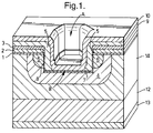
- the active area of the IGBT device shown in Figures 1 and 2 consists of an array of emitter cell cut through windows in a polysilicon gate area.
- the active area of the Power Device is that portion responsible for controlling the current flow. This consists of an array of small cells (usually numbering several thousand) all acting in parallel to give a required total current handling capability.
- Figure 1 shows a section through one such cell, and Figure 2 a cross section through two adjacent cells. Each cell is made up of an emitter region (A) surrounded by polysilicon gate areas. In the on-state current flows from the emitter to the collector (13) located on the back side of the wafer.
- the following description relates to this active portion of the device, the other areas of the device concerned with high voltage junction termination and connection to the gate are not described or shown.
- the IGBT has a substrate 12 of bulk silicon and an epitaxial silicon layer 14.
- the silicon substrate 12 is provided with a metal electric contact layer 13 which acts as the collector for the IGBT and would act as the drain in the case of the invention being applied to a MOSFET.
- the thickness of the epitaxial layer 14 depends upon the voltage drop required.
- the epitaxial layer 14 is n type and the bulk silicon 12 is p type.
- the emitter of the cell is recessed at A and is formed by aluminium metallisation layer 10.
- the gate of the IGBT cell is formed by gate oxide layer 1 and gate conductor layer 2.
- the source of the IGBT comprises the diffusion area 6 which is electrically connected to the base of the recess A by a silicide layer 8.
- passivating layer 5 which should be considered to be distinct from layer 3 as these two layers are formed at different stages in the overall process.
- the layer diagrammatically indicated at 7 is a second dose of the implant 4.
- the essence of the construction according to the present invention is the combination of the recessed emitter structure, the silicide layer 8 and the overlay metallisation 10.
- a deposited insulating layer 9 is used to coat the gate areas in the recess side walls to allow aluminium metallisation 10 to overlay the gate and make contact with the base of each emitter cell. This metal layer need only make contact at the centre of each cell as the silicide layer 8 is relied upon to distribute current beneath the insulating layer 9 to the source regions 6.
- the diffusions of each cell and the silicide strap are produced by self aligned techniques.
- a bulk silicon substrate 12 has an epitaxial silicon layer 14 formed on it.
- the thickness, and resistivity, of this epitaxial layer depends on the desired reverse voltage required.
- This layer 14 may be high resistance epitaxially grown Si on top of a single crystal silicon of the opposite type 12. Alternatively it could comprise an homogeneous high resistivity wafer 14 with layer 12 produced by doping with the opposite type by conventional processes at some stage during the processing.
- MOSFET layers 14 and 12 are of the same type and in the case of IGBT layers 14 and 12 are of opposite type.
- the substrate 12 is p type and the epitaxial layer 14 is n type.
- the first step is to grow a gate oxide 1 on the exposed epitaxial silicon surface 14.
- This oxide layer could typically be 400 to 2,000 ⁇ thick, this step being shown in Figure 4.
- the next step is shown in Figure 5 and comprises the deposition, by standard semiconductor techniques, of a conductive polysilicon layer 2 which will form the gate of the device.
- the next step shown in Figure 6, consists in providing a masking layer 3 which could be an oxide and which could be thermally grown or deposited on top of the polysilicon gate layer 2.
- the layer 3 must be thick enough to act as a mask during subsequent diffusion, implant and etching processes.
- FIG. 7 The next step is shown in Figure 7 where windows W are etched in the multi-layer 1, 2, 3, down to the substrate 14, using standard photolithographic and etching techniques.
- the array of cells thus formed could typically be 5 to 30 ⁇ m wide with similar spacing between the cells. These cells are produced over the active area of the device.
- FIG 8 The next stage in the process is shown in Figure 8 and this consists of an implant/diffusion step.
- an implant/diffusion 4 is carried out, this being of opposite type to the substrate 14, typically 2E14.
- the implant/diffusion takes place through the windows W which have previously been formed.
- the depth of the implant/diffusion 4 could typically be 2-6 ⁇ m.
- the upper oxide layer 3 acts as a mask and defines the extent of the diffusion under the mask edge.
- the sidewalls are passivated by the formation of oxide layer 5 in order to fully insulate the gate polysilicon.
- the layer 5 may be generated by well known deposition and etch techniques.
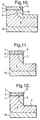
- the next stage, shown in Figure 9, is to remove the passivation layer 5a (see Figure 8) which has formed on the base of the windows W.
- Figure 10 is an enlarged fragmentary view of the arrangement shown in Figure 9, the dimensions being exaggerated in order to facilitate an understanding of the process.
- a highly selective anisotropic silicon plasma etch results in a recess 16 shown in Figure 10.
- the recesses 16 are formed below the level of the gate oxide 1 and the walls of these recesses should ideally be vertical. Again the upper oxide layer forms a mask defining and aligning the recess to the diffusions.
- the diffusion 6 is into the side and bottom of the recess or window W and is of sufficient surface concentration to allow the formation of a low resistance electrical contact on the side wall and with sufficient depth to form the source of the MOSFET beneath the gate oxide 1.
- the depth of the diffusion 6 must not exceed that of the diffusion 4 and can be as shallow as 0.5 ⁇ m or less into the side walls of the recess or window. This thus eliminates unwanted parasitic effects such as latch-up in the case of the IGBT.
- Figure 12 illustrates the next step in the process in which an implant 7, of the same type as diffusion 4, is carried out to form the area shown at the base of the window W.
- the side wall of the window recess is not significantly affected by this process as its walls are vertical and the implant is from the vertical. Again the upper oxide layer 3 forms a mask during this step.
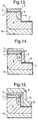
- FIG. 13 The next step is shown in Figure 13 in which a self-aligned metal silicide layer 8 is then formed in the window or recess W using standard semiconductor techniques. Further information on the self-aligned silicide process is disclosed in C.M. Osburn; Q.F. Wang; M. Kellan; C. Canovai; P.L. Smith; G.E. McGuire; Z.G. Xiao; G.A. Rozonyi. "Incorporation of Metal Silicides and Refractory Metals in VLSI Technology". Applied Surface Science 53(1991) p291-312. Proceedings of the 4th European Workshop on Refractory Metals and Silicides 1991.
- the metal silicide 8 which is formed not only on the base but on the side walls of the recess or window W, electrically connects together the diffusions 4 and 6, the layer 8 being of relatively low electrical resistance, typically 13-15m ⁇ -cm.
- the effective short circuit between the regions 4 and 6 eliminates parasitic effects such as latch-up in the case of the IGBT, or lower breakdown voltage in the case where the invention is used to manufacture a MOSFET (see Figure 17 and corresponding description).
- Figure 14 illustrates the next step in the process which is to provide an insulating layer 9 to protect the polysilicon gate 2 from the subsequent metal deposition.
- the insulating oxide 9 would initially also cover the base of the recess/window W but this base covering is then removed using normal photolithographic and etching techniques. It should be noted that this is the only lithographic stage carried out within the recess/windows W, all the other steps within this area employing self-aligning techniques. The advantage of this is that it allows the cell openings W to be reduced in size to about 5 ⁇ m to thus optimize the device's performance.
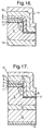
- the next step in the process, illustrated in Figure 15, is to provide a metal deposition 10 over all areas.
- the metal may typically be aluminium.
- a pattern is defined in the metal layer 10 by normal photolithographic and etching techniques so that the emitter areas, or cells, are interconnected by a metal layer or plate that covers the whole active area.
- the aluminium of the metal layer 10 is not required to contact the recess/window W walls as current is distributed by the silicide layer 8 to diffusions 6 and 4.
- the gate area 1, 2 is insulated by the oxide layer 9.
- a passivating layer or layers 11 is/are then deposited covering all areas, including the recess/window side walls, as shown in Figure 16. It should be noted that the layer 11 is not shown in Figures 1 and 2.
- Contact windows are opened to the gate and source pad areas using normal photolithographic and etching techniques.
- metal layers 13 are deposited onto the underside of the silicon substrate 12 to ensure good electrical contact, as shown in Figure 17.
- the layer 13 will form the collector of the device and in the case of a MOSFET the layer 13 will form the drain.
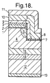
- the present invention may also be used to manufacture an MCT device, as indicated earlier, in which case an extra diffusion layer 15 would be included, as shown in Figure 18, this diffusion layer being of the same type as the diffusion layer 4.
- One advantage of the process of the present invention is that because self-aligning techniques are used smaller emitter windows may be reliably fabricated without the need for the use of highly accurate photolithographic methods.
Landscapes
- Electrodes Of Semiconductors (AREA)
- Thyristors (AREA)
- Insulated Gate Type Field-Effect Transistor (AREA)
Applications Claiming Priority (2)
| Application Number | Priority Date | Filing Date | Title |
|---|---|---|---|
| GB9514996A GB2303487A (en) | 1995-07-21 | 1995-07-21 | Semiconductor devices with recessed emitters |
| GB9514996 | 1995-07-21 |
Publications (1)
| Publication Number | Publication Date |
|---|---|
| EP0755077A2 true EP0755077A2 (fr) | 1997-01-22 |
Family
ID=10778065
Family Applications (1)
| Application Number | Title | Priority Date | Filing Date |
|---|---|---|---|
| EP96305130A Withdrawn EP0755077A2 (fr) | 1995-07-21 | 1996-07-12 | Dispositif de haute puissance à grille MOS et leurs méthodes de fabrication |
Country Status (3)
| Country | Link |
|---|---|
| EP (1) | EP0755077A2 (fr) |
| JP (1) | JPH09121054A (fr) |
| GB (1) | GB2303487A (fr) |
Cited By (6)
| Publication number | Priority date | Publication date | Assignee | Title |
|---|---|---|---|---|
| US6200868B1 (en) | 1997-07-31 | 2001-03-13 | Toyota Jidosha Kabushiki Kaisha | Insulated gate type semiconductor device and process for producing the device |
| US6373103B1 (en) * | 2000-03-31 | 2002-04-16 | Advanced Micro Devices, Inc. | Semiconductor-on-insulator body-source contact using additional drain-side spacer, and method |
| US6441434B1 (en) * | 2000-03-31 | 2002-08-27 | Advanced Micro Devices, Inc. | Semiconductor-on-insulator body-source contact and method |
| US6525381B1 (en) | 2000-03-31 | 2003-02-25 | Advanced Micro Devices, Inc. | Semiconductor-on-insulator body-source contact using shallow-doped source, and method |
| CN104425246A (zh) * | 2013-08-27 | 2015-03-18 | 无锡华润上华半导体有限公司 | 绝缘栅双极型晶体管及其制备方法 |
| CN104425247A (zh) * | 2013-08-27 | 2015-03-18 | 无锡华润上华半导体有限公司 | 一种绝缘栅双极型晶体管的制备方法 |
Family Cites Families (4)
| Publication number | Priority date | Publication date | Assignee | Title |
|---|---|---|---|---|
| DE3380136D1 (en) * | 1982-04-12 | 1989-08-03 | Gen Electric | Semiconductor device having a diffused region of reduced length and method of fabricating the same |
| EP0202477A3 (fr) * | 1985-04-24 | 1988-04-20 | General Electric Company | Procédé pour former des courts-circuits électriques entre des régions voisines dans un dispositif semi-conducteur à gâchette isolée |
| US4885623A (en) * | 1987-10-30 | 1989-12-05 | Holm Kennedy James W | Distributed channel-bipolar device |
| GB2227605A (en) * | 1989-01-30 | 1990-08-01 | Philips Electronic Associated | A vertical field effect semiconductor device |
-
1995
- 1995-07-21 GB GB9514996A patent/GB2303487A/en not_active Withdrawn
-
1996
- 1996-07-12 EP EP96305130A patent/EP0755077A2/fr not_active Withdrawn
- 1996-07-15 JP JP8184908A patent/JPH09121054A/ja active Pending
Cited By (12)
| Publication number | Priority date | Publication date | Assignee | Title |
|---|---|---|---|---|
| US6200868B1 (en) | 1997-07-31 | 2001-03-13 | Toyota Jidosha Kabushiki Kaisha | Insulated gate type semiconductor device and process for producing the device |
| US6373103B1 (en) * | 2000-03-31 | 2002-04-16 | Advanced Micro Devices, Inc. | Semiconductor-on-insulator body-source contact using additional drain-side spacer, and method |
| US6441434B1 (en) * | 2000-03-31 | 2002-08-27 | Advanced Micro Devices, Inc. | Semiconductor-on-insulator body-source contact and method |
| US6525381B1 (en) | 2000-03-31 | 2003-02-25 | Advanced Micro Devices, Inc. | Semiconductor-on-insulator body-source contact using shallow-doped source, and method |
| US6790750B1 (en) | 2000-03-31 | 2004-09-14 | Advanced Micro Devices, Inc. | Semiconductor-on-insulator body-source contact and method |
| CN104425246A (zh) * | 2013-08-27 | 2015-03-18 | 无锡华润上华半导体有限公司 | 绝缘栅双极型晶体管及其制备方法 |
| CN104425247A (zh) * | 2013-08-27 | 2015-03-18 | 无锡华润上华半导体有限公司 | 一种绝缘栅双极型晶体管的制备方法 |
| US9590029B2 (en) | 2013-08-27 | 2017-03-07 | Csmc Technologies Fab1 Co., Ltd. | Method for manufacturing insulated gate bipolar transistor |
| CN104425246B (zh) * | 2013-08-27 | 2018-01-23 | 无锡华润上华科技有限公司 | 绝缘栅双极型晶体管及其制备方法 |
| CN104425247B (zh) * | 2013-08-27 | 2018-01-23 | 无锡华润上华科技有限公司 | 一种绝缘栅双极型晶体管的制备方法 |
| US9881994B2 (en) | 2013-08-27 | 2018-01-30 | CSMC Technologies Fabl Co., Ltd. | Insulated gate bipolar transistor and manufacturing method therefor |
| US10084036B2 (en) | 2013-08-27 | 2018-09-25 | Csmc Technologies Fab1 Co., Ltd. | Insulated gate bipolar transistor and manufacturing method therefor |
Also Published As
| Publication number | Publication date |
|---|---|
| GB9514996D0 (en) | 1995-09-20 |
| GB2303487A (en) | 1997-02-19 |
| JPH09121054A (ja) | 1997-05-06 |
Similar Documents
| Publication | Publication Date | Title |
|---|---|---|
| US5897343A (en) | Method of making a power switching trench MOSFET having aligned source regions | |
| US5731604A (en) | Semiconductor device MOS gated | |
| US6825105B2 (en) | Manufacture of semiconductor devices with Schottky barriers | |
| US6624030B2 (en) | Method of fabricating power rectifier device having a laterally graded P-N junction for a channel region | |
| US5528063A (en) | Conductive-overlaid self-aligned MOS-gated semiconductor devices | |
| US20020074585A1 (en) | Self-aligned power MOSFET with enhanced base region | |
| US20010023104A1 (en) | Field effect transistor and method of its manufacture | |
| US5382536A (en) | Method of fabricating lateral DMOS structure | |
| US6861703B2 (en) | Semiconductor device and method for fabricating the same | |
| US6649973B2 (en) | Semiconductor device and method for manufacturing the same | |
| JPH0758333A (ja) | 電力用mosfet及びその製造方法 | |
| JP2000156503A (ja) | Mosゲートデバイスおよびその製造プロセス | |
| US4845051A (en) | Buried gate JFET | |
| US6548864B2 (en) | High density MOS technology power device | |
| US6207974B1 (en) | Process for manufacture of a p-channel MOS gated device with base implant through the contact window | |
| US5970344A (en) | Method of manufacturing semiconductor device having gate electrodes formed in trench structure before formation of source layers | |
| US6570218B1 (en) | MOSFET with a buried gate | |
| US7189621B2 (en) | Semiconductor device and method for fabricating the same | |
| US6022790A (en) | Semiconductor process integration of a guard ring structure | |
| JPH0286136A (ja) | 半導体素子およびその製造方法 | |
| EP0755077A2 (fr) | Dispositif de haute puissance à grille MOS et leurs méthodes de fabrication | |
| US6090716A (en) | Method of fabricating a field effect transistor | |
| JPH0555583A (ja) | 絶縁ゲート型バイポーラトランジスタの製造方法 | |
| US6541318B2 (en) | Manufacturing process of a high integration density power MOS device | |
| AU698654C (en) | Process for manufacture of mos gated device with reduced mask count |
Legal Events
| Date | Code | Title | Description |
|---|---|---|---|
| PUAI | Public reference made under article 153(3) epc to a published international application that has entered the european phase |
Free format text: ORIGINAL CODE: 0009012 |
|
| AK | Designated contracting states |
Kind code of ref document: A2 Designated state(s): AT DE ES FR GB IT |
|
| STAA | Information on the status of an ep patent application or granted ep patent |
Free format text: STATUS: THE APPLICATION HAS BEEN WITHDRAWN |
|
| 18W | Application withdrawn |
Withdrawal date: 19970716 |