EP0762374B1 - Commande active pour matrices de diodes électroluminescentes - Google Patents
Commande active pour matrices de diodes électroluminescentes Download PDFInfo
- Publication number
- EP0762374B1 EP0762374B1 EP96111992A EP96111992A EP0762374B1 EP 0762374 B1 EP0762374 B1 EP 0762374B1 EP 96111992 A EP96111992 A EP 96111992A EP 96111992 A EP96111992 A EP 96111992A EP 0762374 B1 EP0762374 B1 EP 0762374B1
- Authority
- EP
- European Patent Office
- Prior art keywords
- light emitting
- matrix
- emitting devices
- voltage source
- activating
- Prior art date
- Legal status (The legal status is an assumption and is not a legal conclusion. Google has not performed a legal analysis and makes no representation as to the accuracy of the status listed.)
- Expired - Lifetime
Links
- 239000011159 matrix material Substances 0.000 claims description 58
- 230000003213 activating effect Effects 0.000 claims description 14
- 239000004065 semiconductor Substances 0.000 claims description 13
- 238000000034 method Methods 0.000 claims description 8
- 230000001174 ascending effect Effects 0.000 claims description 2
- 230000004913 activation Effects 0.000 claims 2
- 239000003990 capacitor Substances 0.000 description 5
- 238000004891 communication Methods 0.000 description 5
- 238000004519 manufacturing process Methods 0.000 description 4
- 230000001413 cellular effect Effects 0.000 description 3
- 239000003086 colorant Substances 0.000 description 3
- 238000010586 diagram Methods 0.000 description 3
- 230000001360 synchronised effect Effects 0.000 description 2
- 238000003491 array Methods 0.000 description 1
- 230000001419 dependent effect Effects 0.000 description 1
- 238000012986 modification Methods 0.000 description 1
- 230000004048 modification Effects 0.000 description 1
- 238000012163 sequencing technique Methods 0.000 description 1
Images
Classifications
-
- G—PHYSICS
- G09—EDUCATION; CRYPTOGRAPHY; DISPLAY; ADVERTISING; SEALS
- G09G—ARRANGEMENTS OR CIRCUITS FOR CONTROL OF INDICATING DEVICES USING STATIC MEANS TO PRESENT VARIABLE INFORMATION
- G09G3/00—Control arrangements or circuits, of interest only in connection with visual indicators other than cathode-ray tubes
- G09G3/20—Control arrangements or circuits, of interest only in connection with visual indicators other than cathode-ray tubes for presentation of an assembly of a number of characters, e.g. a page, by composing the assembly by combination of individual elements arranged in a matrix no fixed position being assigned to or needed to be assigned to the individual characters or partial characters
- G09G3/2007—Display of intermediate tones
- G09G3/2011—Display of intermediate tones by amplitude modulation
-
- H—ELECTRICITY
- H10—SEMICONDUCTOR DEVICES; ELECTRIC SOLID-STATE DEVICES NOT OTHERWISE PROVIDED FOR
- H10H—INORGANIC LIGHT-EMITTING SEMICONDUCTOR DEVICES HAVING POTENTIAL BARRIERS
- H10H20/00—Individual inorganic light-emitting semiconductor devices having potential barriers, e.g. light-emitting diodes [LED]
- H10H20/80—Constructional details
-
- G—PHYSICS
- G09—EDUCATION; CRYPTOGRAPHY; DISPLAY; ADVERTISING; SEALS
- G09G—ARRANGEMENTS OR CIRCUITS FOR CONTROL OF INDICATING DEVICES USING STATIC MEANS TO PRESENT VARIABLE INFORMATION
- G09G3/00—Control arrangements or circuits, of interest only in connection with visual indicators other than cathode-ray tubes
- G09G3/20—Control arrangements or circuits, of interest only in connection with visual indicators other than cathode-ray tubes for presentation of an assembly of a number of characters, e.g. a page, by composing the assembly by combination of individual elements arranged in a matrix no fixed position being assigned to or needed to be assigned to the individual characters or partial characters
- G09G3/22—Control arrangements or circuits, of interest only in connection with visual indicators other than cathode-ray tubes for presentation of an assembly of a number of characters, e.g. a page, by composing the assembly by combination of individual elements arranged in a matrix no fixed position being assigned to or needed to be assigned to the individual characters or partial characters using controlled light sources
- G09G3/30—Control arrangements or circuits, of interest only in connection with visual indicators other than cathode-ray tubes for presentation of an assembly of a number of characters, e.g. a page, by composing the assembly by combination of individual elements arranged in a matrix no fixed position being assigned to or needed to be assigned to the individual characters or partial characters using controlled light sources using electroluminescent panels
- G09G3/32—Control arrangements or circuits, of interest only in connection with visual indicators other than cathode-ray tubes for presentation of an assembly of a number of characters, e.g. a page, by composing the assembly by combination of individual elements arranged in a matrix no fixed position being assigned to or needed to be assigned to the individual characters or partial characters using controlled light sources using electroluminescent panels semiconductive, e.g. using light-emitting diodes [LED]
- G09G3/3208—Control arrangements or circuits, of interest only in connection with visual indicators other than cathode-ray tubes for presentation of an assembly of a number of characters, e.g. a page, by composing the assembly by combination of individual elements arranged in a matrix no fixed position being assigned to or needed to be assigned to the individual characters or partial characters using controlled light sources using electroluminescent panels semiconductive, e.g. using light-emitting diodes [LED] organic, e.g. using organic light-emitting diodes [OLED]
- G09G3/3225—Control arrangements or circuits, of interest only in connection with visual indicators other than cathode-ray tubes for presentation of an assembly of a number of characters, e.g. a page, by composing the assembly by combination of individual elements arranged in a matrix no fixed position being assigned to or needed to be assigned to the individual characters or partial characters using controlled light sources using electroluminescent panels semiconductive, e.g. using light-emitting diodes [LED] organic, e.g. using organic light-emitting diodes [OLED] using an active matrix
- G09G3/3258—Control arrangements or circuits, of interest only in connection with visual indicators other than cathode-ray tubes for presentation of an assembly of a number of characters, e.g. a page, by composing the assembly by combination of individual elements arranged in a matrix no fixed position being assigned to or needed to be assigned to the individual characters or partial characters using controlled light sources using electroluminescent panels semiconductive, e.g. using light-emitting diodes [LED] organic, e.g. using organic light-emitting diodes [OLED] using an active matrix with pixel circuitry controlling the voltage across the light-emitting element
-
- G—PHYSICS
- G09—EDUCATION; CRYPTOGRAPHY; DISPLAY; ADVERTISING; SEALS
- G09G—ARRANGEMENTS OR CIRCUITS FOR CONTROL OF INDICATING DEVICES USING STATIC MEANS TO PRESENT VARIABLE INFORMATION
- G09G3/00—Control arrangements or circuits, of interest only in connection with visual indicators other than cathode-ray tubes
- G09G3/20—Control arrangements or circuits, of interest only in connection with visual indicators other than cathode-ray tubes for presentation of an assembly of a number of characters, e.g. a page, by composing the assembly by combination of individual elements arranged in a matrix no fixed position being assigned to or needed to be assigned to the individual characters or partial characters
- G09G3/22—Control arrangements or circuits, of interest only in connection with visual indicators other than cathode-ray tubes for presentation of an assembly of a number of characters, e.g. a page, by composing the assembly by combination of individual elements arranged in a matrix no fixed position being assigned to or needed to be assigned to the individual characters or partial characters using controlled light sources
- G09G3/30—Control arrangements or circuits, of interest only in connection with visual indicators other than cathode-ray tubes for presentation of an assembly of a number of characters, e.g. a page, by composing the assembly by combination of individual elements arranged in a matrix no fixed position being assigned to or needed to be assigned to the individual characters or partial characters using controlled light sources using electroluminescent panels
- G09G3/32—Control arrangements or circuits, of interest only in connection with visual indicators other than cathode-ray tubes for presentation of an assembly of a number of characters, e.g. a page, by composing the assembly by combination of individual elements arranged in a matrix no fixed position being assigned to or needed to be assigned to the individual characters or partial characters using controlled light sources using electroluminescent panels semiconductive, e.g. using light-emitting diodes [LED]
- G09G3/3208—Control arrangements or circuits, of interest only in connection with visual indicators other than cathode-ray tubes for presentation of an assembly of a number of characters, e.g. a page, by composing the assembly by combination of individual elements arranged in a matrix no fixed position being assigned to or needed to be assigned to the individual characters or partial characters using controlled light sources using electroluminescent panels semiconductive, e.g. using light-emitting diodes [LED] organic, e.g. using organic light-emitting diodes [OLED]
- G09G3/3275—Details of drivers for data electrodes
- G09G3/3291—Details of drivers for data electrodes in which the data driver supplies a variable data voltage for setting the current through, or the voltage across, the light-emitting elements
-
- G—PHYSICS
- G09—EDUCATION; CRYPTOGRAPHY; DISPLAY; ADVERTISING; SEALS
- G09G—ARRANGEMENTS OR CIRCUITS FOR CONTROL OF INDICATING DEVICES USING STATIC MEANS TO PRESENT VARIABLE INFORMATION
- G09G2300/00—Aspects of the constitution of display devices
- G09G2300/04—Structural and physical details of display devices
- G09G2300/0439—Pixel structures
- G09G2300/0465—Improved aperture ratio, e.g. by size reduction of the pixel circuit, e.g. for improving the pixel density or the maximum displayable luminance or brightness
-
- G—PHYSICS
- G09—EDUCATION; CRYPTOGRAPHY; DISPLAY; ADVERTISING; SEALS
- G09G—ARRANGEMENTS OR CIRCUITS FOR CONTROL OF INDICATING DEVICES USING STATIC MEANS TO PRESENT VARIABLE INFORMATION
- G09G2300/00—Aspects of the constitution of display devices
- G09G2300/08—Active matrix structure, i.e. with use of active elements, inclusive of non-linear two terminal elements, in the pixels together with light emitting or modulating elements
- G09G2300/0804—Sub-multiplexed active matrix panel, i.e. wherein one active driving circuit is used at pixel level for multiple image producing elements
-
- G—PHYSICS
- G09—EDUCATION; CRYPTOGRAPHY; DISPLAY; ADVERTISING; SEALS
- G09G—ARRANGEMENTS OR CIRCUITS FOR CONTROL OF INDICATING DEVICES USING STATIC MEANS TO PRESENT VARIABLE INFORMATION
- G09G2300/00—Aspects of the constitution of display devices
- G09G2300/08—Active matrix structure, i.e. with use of active elements, inclusive of non-linear two terminal elements, in the pixels together with light emitting or modulating elements
- G09G2300/0809—Several active elements per pixel in active matrix panels
- G09G2300/0842—Several active elements per pixel in active matrix panels forming a memory circuit, e.g. a dynamic memory with one capacitor
-
- G—PHYSICS
- G09—EDUCATION; CRYPTOGRAPHY; DISPLAY; ADVERTISING; SEALS
- G09G—ARRANGEMENTS OR CIRCUITS FOR CONTROL OF INDICATING DEVICES USING STATIC MEANS TO PRESENT VARIABLE INFORMATION
- G09G2310/00—Command of the display device
- G09G2310/02—Addressing, scanning or driving the display screen or processing steps related thereto
- G09G2310/0235—Field-sequential colour display
-
- G—PHYSICS
- G09—EDUCATION; CRYPTOGRAPHY; DISPLAY; ADVERTISING; SEALS
- G09G—ARRANGEMENTS OR CIRCUITS FOR CONTROL OF INDICATING DEVICES USING STATIC MEANS TO PRESENT VARIABLE INFORMATION
- G09G2310/00—Command of the display device
- G09G2310/02—Addressing, scanning or driving the display screen or processing steps related thereto
- G09G2310/0243—Details of the generation of driving signals
- G09G2310/0254—Control of polarity reversal in general, other than for liquid crystal displays
- G09G2310/0256—Control of polarity reversal in general, other than for liquid crystal displays with the purpose of reversing the voltage across a light emitting or modulating element within a pixel
-
- G—PHYSICS
- G09—EDUCATION; CRYPTOGRAPHY; DISPLAY; ADVERTISING; SEALS
- G09G—ARRANGEMENTS OR CIRCUITS FOR CONTROL OF INDICATING DEVICES USING STATIC MEANS TO PRESENT VARIABLE INFORMATION
- G09G2310/00—Command of the display device
- G09G2310/02—Addressing, scanning or driving the display screen or processing steps related thereto
- G09G2310/0264—Details of driving circuits
- G09G2310/027—Details of drivers for data electrodes, the drivers handling digital grey scale data, e.g. use of D/A converters
-
- G—PHYSICS
- G09—EDUCATION; CRYPTOGRAPHY; DISPLAY; ADVERTISING; SEALS
- G09G—ARRANGEMENTS OR CIRCUITS FOR CONTROL OF INDICATING DEVICES USING STATIC MEANS TO PRESENT VARIABLE INFORMATION
- G09G2320/00—Control of display operating conditions
- G09G2320/04—Maintaining the quality of display appearance
- G09G2320/043—Preventing or counteracting the effects of ageing
-
- G—PHYSICS
- G09—EDUCATION; CRYPTOGRAPHY; DISPLAY; ADVERTISING; SEALS
- G09G—ARRANGEMENTS OR CIRCUITS FOR CONTROL OF INDICATING DEVICES USING STATIC MEANS TO PRESENT VARIABLE INFORMATION
- G09G2330/00—Aspects of power supply; Aspects of display protection and defect management
- G09G2330/02—Details of power systems and of start or stop of display operation
-
- G—PHYSICS
- G09—EDUCATION; CRYPTOGRAPHY; DISPLAY; ADVERTISING; SEALS
- G09G—ARRANGEMENTS OR CIRCUITS FOR CONTROL OF INDICATING DEVICES USING STATIC MEANS TO PRESENT VARIABLE INFORMATION
- G09G3/00—Control arrangements or circuits, of interest only in connection with visual indicators other than cathode-ray tubes
- G09G3/20—Control arrangements or circuits, of interest only in connection with visual indicators other than cathode-ray tubes for presentation of an assembly of a number of characters, e.g. a page, by composing the assembly by combination of individual elements arranged in a matrix no fixed position being assigned to or needed to be assigned to the individual characters or partial characters
- G09G3/2007—Display of intermediate tones
- G09G3/2018—Display of intermediate tones by time modulation using two or more time intervals
- G09G3/2022—Display of intermediate tones by time modulation using two or more time intervals using sub-frames
- G09G3/2025—Display of intermediate tones by time modulation using two or more time intervals using sub-frames the sub-frames having all the same time duration
-
- G—PHYSICS
- G09—EDUCATION; CRYPTOGRAPHY; DISPLAY; ADVERTISING; SEALS
- G09G—ARRANGEMENTS OR CIRCUITS FOR CONTROL OF INDICATING DEVICES USING STATIC MEANS TO PRESENT VARIABLE INFORMATION
- G09G3/00—Control arrangements or circuits, of interest only in connection with visual indicators other than cathode-ray tubes
- G09G3/20—Control arrangements or circuits, of interest only in connection with visual indicators other than cathode-ray tubes for presentation of an assembly of a number of characters, e.g. a page, by composing the assembly by combination of individual elements arranged in a matrix no fixed position being assigned to or needed to be assigned to the individual characters or partial characters
- G09G3/2007—Display of intermediate tones
- G09G3/2077—Display of intermediate tones by a combination of two or more gradation control methods
- G09G3/2081—Display of intermediate tones by a combination of two or more gradation control methods with combination of amplitude modulation and time modulation
Definitions
- the present invention pertains to active matrices and more specifically to new apparatus and methods of driving active matrices.
- Displays utilizing two dimensional arrays, or matrices, of pixels each containing one or more light emitting devices are very popular in the electronics field and especially in portable electronic and communication devices, because large amounts of data and pictures can be transmitted very rapidly and to virtually any location.
- One problem with these matrices is that each row (or column) of light emitting devices in the matrix must be separately addressed and driven with a video or data driver.
- US 5386179 A1 (SATO) describes means for current switching within electroluminescent devices arranged in rows and columns by supplying scan and image data, the image data activating signal determining when a pixel is activated.
- each pixel contains a single light emitting device which must be driven in a range of values to achieve a range of gray (gray scale) between full on (white) and full off (black).
- the data drivers In order to get good gray scale, the data drivers generally have to be able to deliver an accurate analog voltage to each pixel.
- analog driver circuits are very expensive and, since there must be hundreds of data drivers (one for each column of light emitting devices), are the major part of the display cost.
- each pixel contains at least three light emitting devices, each of which produces a different color (e.g. red, green and blue) and each of which must be driven (generally a row at a time) in a range of values to achieve a range of that specific color between full on and full off.
- full color displays contain three times as many analog drivers, which triples the manufacturing cost of the display.
- the additional analog drivers require additional space and power, which can be a problem in portable electronic devices, such as pagers, cellular and regular telephones, radios, data banks, etc.
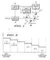
- FIG. 1 a simplified block/schematic drawing is illustrated showing an active driven light emitting diode matrix.
- a single light emitting diode 10 is illustrated but it will be understood that diode 10 is simply one diode in a two dimensional array including rows and columns of light emitting diodes.
- light emitting diode 10 and each other diode in the matrix has a semiconductor switch 12 attached thereto, making the matrix an active matrix.
- switch 12 includes a first transistor 13 having a current carrying electrode 14 connected to the cathode of diode 10 and a current carrying electrode 15 connected to a common return, such as ground or the like.
- Switch 12 further includes a second transistor 18 having a current carrying terminal 19 connected to a gate or control terminal 20 of transistor 13.
- a second current carrying terminal 21 of transistor 18 serves as a data input and a gate or control terminal 22 serves as an input for scan signals.
- a capacitor 23 is connected between control terminal 20 and the common return or ground as a storage element to maintain diode 10 in an ON mode for a specific period of time after switching.
- light emitting diode 10 and switch 12 form a pixel.
- light emitting diode 10 is an organic light emitting diode, which is a current driven device, so that switch 12 is a low operating voltage device.
- Light emitting diode 10 is addressed by supplying a scan signal to control terminal 22 of transistor 18 and a data signal to current terminal 21. Depending upon the data signal, when transistor 13 is activated a current path is completed between the cathode of light emitting diode 10 and the common return, or ground.
- Each current carrying terminal 21 for each switch 12 in each pixel in a column are connected together and to a data driver 25. While transistors 13 and 18 are illustrated as n-type devices, it will be understood by those skilled in the art that diodes 10 could be reversed and p-type devices could be used in switch 12, if desired.
- data drivers 25 there may be 640 columns by 480 rows of pixels.
- data drivers 25 there are 640 data drivers 25.
- the matrix could be rotated ninety degrees so that the scan signals and data signals are supplied to columns and rows, respectively, if desired.
- data drivers 25 are relatively simple digital drivers in this embodiment, for reasons that will become apparent presently.
- Data is supplied to a data input of each data driver 25, which data may be, for example, received from a wireless communication or from some data bank or storage device and may represent alpha-numeric and/or graphic information.
- Control terminal 22 of each switch 12 in a row of pixels are connected together and to a circuit for supplying scan signals thereto.
- a shift register 27 is provided to supply the scan signals.
- Shift register 27 has a separate output for each row in the matrix (e.g. 480 outputs) and sequentially supplies a scan signal on each output in turn.
- rows 1 through 480 of the matrix are sequentially supplied with a scan signal.
- a scan signal is applied to each row for a sufficient time to allow all of the data drivers to be activated so that each pixel in the row being scanned is addressed.
- a scan signal is then applied to the next row and all of the data drivers are activated, etc. Therefore, each pixel in the matrix is addressed with a scan and data signal by the combination of data drivers 25 and shift register 27.
- a voltage source 30 is provided which is constructed to repetitiously supply a multi-step voltage waveform at an output thereof.
- a typical multi-step voltage waveform is illustrated in FIG. 2, including m ascending steps, or subframes, and each step represents the amount of voltage required to produce the intensity, I, produced by a specific light emitting diode (e.g. diode 10). All of the anodes of the light emitting diodes are connected together and to the output terminal of voltage source 30.
- the entire matrix is addressed to complete a first subframe.
- the data from data drivers 25 includes a digital signal that turns ON each pixel (completes a circuit from the cathode of the diode to ground) that requires a first level or shade of gray.
- a timing circuit 35 is attached to data drivers 25, shift register 27 and voltage source 30 to ensure proper synchronization of the subframes and frames. Also, in instances where the data is communicated through a wireless communication system (e.g. radio, cellular telephone, etc.) timing circuit 35 is synchronized to the incoming data. Thus, by subdividing a frame into m subframes and properly synchronizing voltage source 30 to the scan and data drivers, an m-bit gray scale is achieved using simple digital data drivers.
- a wireless communication system e.g. radio, cellular telephone, etc.
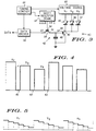
- FIG. 3 a simplified block/schematic diagram is illustrated showing another embodiment of an active driven light emitting diode matrix, which is utilized to produce full color images.
- a single pixel 40 is illustrated but it will be understood that pixel 40 is simply one pixel in a two dimensional array or matrix including rows and columns of pixels.
- Pixel 40, and each other pixel in the matrix has a semiconductor switch 42 attached thereto, making the matrix an active matrix.
- switch 42 includes a first transistor 43 having a current carrying electrode 44 connected in common to the cathodes of three light emitting diodes 45, 46, and 47 and a current carrying electrode 48 connected to a common return, such as ground or the like.
- Switch 42 further includes a second transistor 50 having a current carrying terminal 51 connected to a gate or control terminal 52 of transistor 43.
- a second current carrying terminal 53 of transistor 50 serves as a data input and a gate or control terminal 54 serves as an input for scan signals.
- light emitting diodes 45, 46, and 47 and switch 42 form a pixel. While transistors 43 and 50 are illustrated as n-type devices, it will be understood by those skilled in the art that diodes 45, 46, and 47 could be reversed and p-type devices could be used in switch 42, if desired.
- light emitting diodes 45, 46, and 47 are organic light emitting diodes designed to produce red, green and blue light, respectively, when energized.
- Pixel 40 is addressed by supplying a scan signal to control terminal 54 of transistor 50 and a data signal to current terminal 53. Depending upon the data signal, when transistor 43 is activated a current path is completed between all three cathodes of light emitting diodes 45, 46, and 47 and the common return, or ground.
- Each current carrying terminal 53 for each switch 42 in each pixel in a column are connected together and to a data driver 55.
- a data driver 55 As an example, in a typical matrix containing 640 columns by 480 rows of pixels, there are 640 data drivers 55. Data is supplied to a data input of each data driver 55, which data may be, for example, received from a wireless communication or from some data bank or storage device and may represent alpha-numeric and/or graphic information.
- Control terminal 54 of each switch 42 in a row of pixels are connected together and to a circuit for supplying scan signals thereto.
- a shift register 57 is provided to supply the scan signals.
- Shift register 57 has a separate output for each row in the matrix (e.g. 480 outputs) and sequentially supplies a scan signal on each output in turn.
- rows 1 through 480 of the matrix are sequentially supplied with a scan signal.
- a scan signal is applied to each row for a sufficient time to allow all of the data drivers to be activated so that each pixel in the row being scanned is addressed.
- a scan signal is then applied to the next row and all of the data drivers are activated, etc. Therefore, each pixel in the matrix is addressed by the combination of data drivers 55 and shift register 57.
- a voltage source 60 is provided which is constructed to repetitiously supply voltage to each of three outputs, designated Vr, Vg, and Vb, as illustrated in FIG. 4.
- the anodes of the light emitting diodes 46 in all of the pixels in the matrix are connected together and to output terminal Vg of voltage source 60.
- the anodes of the light emitting diodes 47 in all of the pixels in the matrix are connected together and to output terminal Vb of voltage source 60.
- a first voltage is applied to the output terminal Vr and the entire matrix is addressed to complete a first subframe.
- the entire matrix (all pixels), can be addressed in several well known addressing schemes, for example, by sequencing through the rows, one through n, and supplying data to all of the columns simultaneously in parallel as each row is addressed. Whatever addressing scheme is used, the result is to provide each pixel in the array with a scan and a data signal.
- Data drivers 55 could be analog drivers that turn switches 42 on for a predetermined amplitude or time of current flow through one of diodes 45, 46, or 47 to achieve the amount of each color desired in each pixel.
- a second voltage Vg is applied to the output terminal Vg and the entire matrix is addressed to complete a second subframe.
- a third voltage Vb is applied to the output terminal Vb and the entire matrix is addressed to complete a third subframe. The three subframes form a complete frame and the procedure is repeated at a rate of approximately 60 frames per second.
- each of the voltages Vr, Vg, and Vb has associated therewith a blanking pulse 61, 62, and 63, respectively.
- the blanking pulses are provided before each subframe to allow for the transfer of data into the storage capacitor.
- the next subframe begins with a proper value of data in the storage capacitor when the diode is turned on.
- the negative voltage ensures the complete removal of any charge build-up that may occur in the various circuits.
- a timing circuit 65 is attached to data drivers 55, shift register 57 and voltage source 60 to ensure proper synchronization of the subframes and frames. Also, in instances where the data is communicated through a wireless communication system (e.g. radio, cellular telephone, etc.) timing circuit 65 is synchronized to the incoming data.
- a wireless communication system e.g. radio, cellular telephone, etc.
- timing circuit 65 is synchronized to the incoming data.
- the number of active matrix elements i.e. two FETs and a capacitor
- the number of data drivers is reduced by a factor of three for a full color display. This is a substantial reduction in the size and cost of the matrix and the cost of the drivers.
- FIG. 5 a multi-step voltage waveform is illustrated for a different embodiment of an active driven light emitting diode matrix in accordance with the present invention.
- the waveform of FIG. 5 will be explained in conjunction with the structure of FIG. 3, which again is utilized to produce full color images.
- data drivers 55 are relatively simple digital drivers, rather than the previously described analog drivers, for reasons that will be apparent presently.
- each frame is divided into three subframes Vr, Vg, and Vb and each subframe is divided into m multi-steps of voltage or sub-subframes.
- the multi-step subframe Vr is applied to the Vr output of voltage source 60 and the entire matrix is addressed for each of the m steps. This procedure is continued until all m of the sub-subframes are completed, completing a subframe.
- Voltage source 60 is then switched so that the multi-step subframe Vg is applied to the Vg output.
- the entire matrix is again addressed for each of the m steps and the procedure is continued until all m of the sub-subframes are completed, completing a second subframe.
- the data drivers are simple digital drivers used to turn on switch 42 for a specific time.
- the number of active matrix elements i.e. two FETs and a capacitor
- the number of data drivers is reduced by a factor of three for a full color display and, in addition, the data drivers are greatly simplified. This is a substantial reduction in the cost and number of the data drivers and in the size and cost of the matrix.
- displays and especially color displays, with simpler and/or fewer data drivers have been disclosed.
- relatively simple digital drivers can be used instead of much more complicated and expensive analog drivers, to greatly reduce the cost of displays.
- the disclosed displays incorporate fewer components in the active matrix so that not only are the data drivers reduced in number and simplified but the matrix is also simplified. Further, because the active components in a matrix for a full color display are reduced by one third, the matrix is easier to manufacture and can be made smaller.
Landscapes
- Engineering & Computer Science (AREA)
- Physics & Mathematics (AREA)
- Computer Hardware Design (AREA)
- General Physics & Mathematics (AREA)
- Theoretical Computer Science (AREA)
- Control Of Indicators Other Than Cathode Ray Tubes (AREA)
- Electroluminescent Light Sources (AREA)
- Devices For Indicating Variable Information By Combining Individual Elements (AREA)
- Control Of El Displays (AREA)
Claims (9)
- Appareil d'entraînement actif destiné à une matrice de dispositifs électroluminescents comprenant:une source de tension (30, 60);une matrice comprenant une pluralité de rangées de pixels (10 et 12, 42 et 45, 46, 47) et une pluralité de colonnes de pixels (10 et 12, 42 et 45, 46, 47), chaque pixel comprenant au moins un dispositif électroluminescent (10, 45, 46, 47) chacun dudit ou desdits dispositif(s) électroluminescent(s) ayant un premier contact relié à la source de tension (30, 60) et un second contact;des circuits de synchronisation (35, 65);un registre de décalage (27, 57);un circuit d'entraînement de colonne (25, 55);une pluralité de commutateurs à semi-conducteurs (12, 42), chacun associés à chaque pixel, chaque commutateur à semi-conducteurs (12, 42) ayant une première borne de transport de courant (14, 44) reliée au second contact du dispositif électroluminescent au moins (10, 45, 46, 47) du pixel associé, et une seconde borne de transport de courant (15, 48) reliée à une borne commune, chaque commutateur à semi-conducteurs (12, 42) ayant en outre une première et une seconde bornes d'entrée d'activation (21, 22, 53, 54), et chaque commutateur à semi-conducteurs (12, 42) étant construit afin de réaliser un circuit entre la première et la seconde bornes de transport de courant (13, 15, 43, 48) uniquement lorsque des signaux d'activation sont fournis à la première et à la seconde bornes d'entrée d'activation (21, 22, 53, 54);
dans lequel lesdits circuit de synchronisation (35, 65) sont reliés aux circuits d'entraînement de colonnes (25, 55) et au registre de décalage (27, 57), le circuit de synchronisation (35, 65) étant construit afin de contrôler le registre de décalage (57, 57) de façon à fournir un signal d'activation à chaque rangée en séquence et afin de contrôler chaque circuit d'entraînement de colonne (25, 55) de façon à fournir un signal d'activation à chaque colonne en séquence pour chaque signal d'activation appliqué à une rangée, chaque activation de l'ensemble des rangées de la matrice étant définie comme étant une sous-trame,
caractérisé en ce que
lesdits circuits de synchronisation (35, 65) sont reliés à la source de tension (30, 60) et sont adaptés afin d'activer ladite source de tension;
ladite source de tension (30, 60) est construite afin de fournir de manière répétée une forme d'onde de tension à plusieurs étages (Vs, Vr, Vb) lorsqu'elle est activée; et en ce quele circuit de synchronisation (35, 65) est en outre construit afin de contrôler la source de tension (30, 60) de façon à fournir un étage séquentiel suivant à la forme d'onde de tension à étages multiples (Vs, V, V91 Vb) à chaque fois qu'une sous-trame est réalisée, une trame étant réalisée lorsque l'ensemble des tensions à étages multiples de la forme d'onde est fourni. - Appareil d'entraînement actif destiné à une matrice de dispositifs électroluminescents selon la revendication 1, caractérisé en outre en ce que la forme d'onde de tension à étages multiples (Vs, Vr, Vg, Vb) que la source de tension (30, 60) doit fournir de manière répétée comprend une pluralité d'étages ascendants de tension, représentant chacun un niveau d'une échelle de gris à plusieurs bits.
- Appareil d'entraînement actif destiné à une matrice de dispositifs électroluminescents selon la revendication 1, caractérisé en outre en ce que les dispositifs électroluminescents (10, 45, 46, 47) sont des diodes électroluminescentes organiques.
- Appareil d'entraînement actif destiné à une matrice de dispositifs électroluminescents selon la revendication 1, caractérisé en outre en ce que chacun de la pluralité de commutateurs à semi-conducteurs (12, 42) comprend un premier transistor (13, 43) ayant des électrodes de transport de courant (14, 15, 44, 48) formant la première et la seconde bornes de transport de courant (14, 15, 44, 48) du commutateur à semi-conducteurs (12, 42), et une électrode de commande (20, 52).
- Appareil d'entraînement actif destiné à une matrice de dispositifs électroluminescents selon la revendication 4, caractérisé en outre en ce que chacun de la pluralité de commutateurs à semi-conducteurs (12, 42) comprend en outre un second transistor (18, 50) ayant une première électrode de transport de courant (19, 51) reliée à l'électrode de commande (20, 52) du premier transistor (13, 43), une seconde électrode de transport de courant (21, 53) formant la première borne d'entrée d'activation (21, 53) du commutateur à semi-conducteurs (12, 42), et une borne de commande (22, 54) formant la seconde borne d'entrée d'activation (22, 54) du commutateur à semi-conducteurs (12, 42).
- Appareil d'entraînement actif destiné à une matrice de dispositifs électroluminescents selon la revendication 1, caractérisé en outre en ce que toutes les premières bornes d'activation (21, 53) de chaque commutateur à semi-conducteurs (12, 42) associé aux dispositifs électroluminescents (10, 45, 46, 47) dans chaque colonne spécifique de dispositifs électroluminescents (10, 45, 46, 47) sont reliées ensemble et à un circuit d'entraînement de colonne (25, 55).
- Appareil d'entraînement actif destiné à une matrice de dispositifs électroluminescents selon la revendication 6, caractérisé en outre en ce que chacun des circuits d'entraînement de colonne (25, 55) est un dispositif d'entraînement numérique.
- Appareil d'entraînement actif destiné à une matrice de dispositifs électroluminescents selon la revendication 6, caractérisé en outre en ce que toutes les secondes bornes d'activation (22, 54) de chaque commutateur à semi-conducteurs (12, 42) associé au dispositif électroluminescent (10, 45, 46, 47) dans chaque rangée spécifique de dispositifs électroluminescents (10, 45, 46, 47) sont reliées ensemble et à une sortie du registre de décalage (27, 57).
- Procédé d'entraînement d'une matrice de dispositifs électroluminescents comprenant les étapes consistant à:adresser chaque pixel (10, 40) d'une matrice ayant une pluralité de rangées de pixels (10, 40) et une pluralité de colonnes de pixels (10, 40), chaque pixel (10, 40) comprenant au moins un premier dispositif électroluminescent ayant un premier contact relié à une première sortie d'une source de tension (30, 60) et un second contact, en fournissant des signaux d'activation de données de balayage et d'image (27, 57, 25, 55) à chacun des pixels (10, 40) de la matrice, les signaux d'activation de données d'image (25, 55) étant utilisés afin de déterminer le moment auquel un pixel (10, 40) est activé en réalisant un trajet de courant entre le second contact (14, 44) de chaque pixel (10, 40) et une seconde sortie (15, 48) de la source dé tension (30, 60),caractérisé par les étapes consistant à:activer une source de tension (30, 60) construite afin de fournir de manière répétée une forme d'onde de tension à étages multiples (Vs, Vr, Vg, Vb) lorsqu'elle est activée, de façon à fournir de manière répétée des formes d'onde de tension à étages multiples (Vs, Vr, Vg, Vb) et à fournir séquentiellement chaque étage de chacune des formes d'onde de tension à étages multiples (Vs, Vr, Vg, Vb) aux pixels (10, 40), et adresser chacun des pixels (10, 40) de la matrice pour chaque étage fourni, où chaque activation ou adressage de l'ensemble des pixels (10, 45, 46, 47) de la matrice est une sous-trame;contrôler la source de tension (30, 60) avec un circuit de synchronisation (35, 65) afin de fournir un étage séquentiel suivant de la forme d'onde de tension à étages multiples (Vs, Vr, Vg, Vb) à chaque fois qu'une sous-trame est réalisée, une trame étant réalisée lorsque l'ensemble des tensions à étages multiples de la forme d'onde a été fourni.
Applications Claiming Priority (2)
| Application Number | Priority Date | Filing Date | Title |
|---|---|---|---|
| US517222 | 1983-07-25 | ||
| US08/517,222 US5748160A (en) | 1995-08-21 | 1995-08-21 | Active driven LED matrices |
Publications (2)
| Publication Number | Publication Date |
|---|---|
| EP0762374A1 EP0762374A1 (fr) | 1997-03-12 |
| EP0762374B1 true EP0762374B1 (fr) | 2007-04-04 |
Family
ID=24058894
Family Applications (1)
| Application Number | Title | Priority Date | Filing Date |
|---|---|---|---|
| EP96111992A Expired - Lifetime EP0762374B1 (fr) | 1995-08-21 | 1996-07-25 | Commande active pour matrices de diodes électroluminescentes |
Country Status (6)
| Country | Link |
|---|---|
| US (1) | US5748160A (fr) |
| EP (1) | EP0762374B1 (fr) |
| JP (1) | JPH09138659A (fr) |
| KR (1) | KR100446567B1 (fr) |
| DE (1) | DE69637005T2 (fr) |
| TW (1) | TW366480B (fr) |
Cited By (2)
| Publication number | Priority date | Publication date | Assignee | Title |
|---|---|---|---|---|
| US7903052B2 (en) | 2003-11-14 | 2011-03-08 | Samsung Mobile Display Co., Ltd. | Pixel driving circuit for a display device and a driving method thereof |
| US9082344B2 (en) | 2003-11-25 | 2015-07-14 | Samsung Display Co., Ltd. | Pixel circuit in flat panel display device and method for driving the same |
Families Citing this family (236)
| Publication number | Priority date | Publication date | Assignee | Title |
|---|---|---|---|---|
| US6157356A (en) * | 1996-04-12 | 2000-12-05 | International Business Machines Company | Digitally driven gray scale operation of active matrix OLED displays |
| JP3712802B2 (ja) * | 1996-10-29 | 2005-11-02 | 富士通株式会社 | 中間調表示方法および表示装置 |
| US6545654B2 (en) | 1996-10-31 | 2003-04-08 | Kopin Corporation | Microdisplay for portable communication systems |
| GB9624706D0 (en) * | 1996-11-28 | 1997-01-15 | Cambridge Display Tech Ltd | Light emitting polymer device |
| JPH10161563A (ja) * | 1996-11-29 | 1998-06-19 | Tdk Corp | 有機el表示装置 |
| TW441136B (en) * | 1997-01-28 | 2001-06-16 | Casio Computer Co Ltd | An electroluminescent display device and a driving method thereof |
| US6462722B1 (en) * | 1997-02-17 | 2002-10-08 | Seiko Epson Corporation | Current-driven light-emitting display apparatus and method of producing the same |
| EP1830344B1 (fr) * | 1997-02-17 | 2012-07-04 | Seiko Epson Corporation | Structure d'un circuit de commande d'élément d'image pour un dispositif d'affichage luminescent |
| WO1998048403A1 (fr) * | 1997-04-23 | 1998-10-29 | Sarnoff Corporation | Structure de pixel a diode luminescente a matrice active et procede |
| JP3530341B2 (ja) * | 1997-05-16 | 2004-05-24 | Tdk株式会社 | 画像表示装置 |
| JPH1173158A (ja) | 1997-08-28 | 1999-03-16 | Seiko Epson Corp | 表示素子 |
| JP3767877B2 (ja) * | 1997-09-29 | 2006-04-19 | 三菱化学株式会社 | アクティブマトリックス発光ダイオード画素構造およびその方法 |
| US6232963B1 (en) * | 1997-09-30 | 2001-05-15 | Texas Instruments Incorporated | Modulated-amplitude illumination for spatial light modulator |
| US6266035B1 (en) * | 1997-10-30 | 2001-07-24 | Lear Automotive Dearborn, Inc. | ELD driver with improved brightness control |
| US6552704B2 (en) * | 1997-10-31 | 2003-04-22 | Kopin Corporation | Color display with thin gap liquid crystal |
| US6476784B2 (en) | 1997-10-31 | 2002-11-05 | Kopin Corporation | Portable display system with memory card reader |
| US6909419B2 (en) * | 1997-10-31 | 2005-06-21 | Kopin Corporation | Portable microdisplay system |
| KR100637433B1 (ko) | 2004-05-24 | 2006-10-20 | 삼성에스디아이 주식회사 | 발광 표시 장치 |
| GB9803441D0 (en) * | 1998-02-18 | 1998-04-15 | Cambridge Display Tech Ltd | Electroluminescent devices |
| WO1999048337A1 (fr) | 1998-03-13 | 1999-09-23 | Cambridge Display Technology Ltd. | Dispositifs electroluminescents |
| WO1999053472A1 (fr) * | 1998-04-15 | 1999-10-21 | Cambridge Display Technology Ltd. | Dispositif de commande d'affichage comprenant des modes d'economie de la consommation d'energie |
| JP3568097B2 (ja) * | 1998-04-22 | 2004-09-22 | パイオニア株式会社 | 発光ディスプレイ及びその駆動方法 |
| JP2002529791A (ja) | 1998-11-06 | 2002-09-10 | コピン・コーポレーシヨン | マイクロデイスプレービューワー |
| KR20020006019A (ko) * | 1998-12-14 | 2002-01-18 | 도날드 피. 게일 | 휴대용 마이크로디스플레이 시스템 |
| US6618031B1 (en) | 1999-02-26 | 2003-09-09 | Three-Five Systems, Inc. | Method and apparatus for independent control of brightness and color balance in display and illumination systems |
| MY124036A (en) | 1999-07-08 | 2006-06-30 | Nichia Corp | Image display apparatus and its method of operation |
| TW540251B (en) * | 1999-09-24 | 2003-07-01 | Semiconductor Energy Lab | EL display device and method for driving the same |
| JP4906017B2 (ja) * | 1999-09-24 | 2012-03-28 | 株式会社半導体エネルギー研究所 | 表示装置 |
| US6421033B1 (en) * | 1999-09-30 | 2002-07-16 | Innovative Technology Licensing, Llc | Current-driven emissive display addressing and fabrication scheme |
| JP2001109432A (ja) * | 1999-10-06 | 2001-04-20 | Pioneer Electronic Corp | アクティブマトリックス型発光パネルの駆動装置 |
| TW535454B (en) * | 1999-10-21 | 2003-06-01 | Semiconductor Energy Lab | Electro-optical device |
| US6587086B1 (en) * | 1999-10-26 | 2003-07-01 | Semiconductor Energy Laboratory Co., Ltd. | Electro-optical device |
| US6307322B1 (en) * | 1999-12-28 | 2001-10-23 | Sarnoff Corporation | Thin-film transistor circuitry with reduced sensitivity to variance in transistor threshold voltage |
| US6999057B2 (en) * | 2000-02-22 | 2006-02-14 | Kopin Corporation | Timing of fields of video |
| PT1422975E (pt) * | 2000-04-24 | 2010-07-09 | Philips Solid State Lighting | Produto base de leds |
| CN1201280C (zh) * | 2000-05-22 | 2005-05-11 | 皇家菲利浦电子有限公司 | 有源矩阵电致发光显示设备 |
| TW493153B (en) * | 2000-05-22 | 2002-07-01 | Koninkl Philips Electronics Nv | Display device |
| JP3877049B2 (ja) * | 2000-06-27 | 2007-02-07 | 株式会社日立製作所 | 画像表示装置及びその駆動方法 |
| US6738034B2 (en) | 2000-06-27 | 2004-05-18 | Hitachi, Ltd. | Picture image display device and method of driving the same |
| US6825820B2 (en) * | 2000-08-10 | 2004-11-30 | Semiconductor Energy Laboratory Co., Ltd. | Display device and electronic device |
| US6828950B2 (en) * | 2000-08-10 | 2004-12-07 | Semiconductor Energy Laboratory Co., Ltd. | Display device and method of driving the same |
| JP4884609B2 (ja) * | 2000-08-10 | 2012-02-29 | 株式会社半導体エネルギー研究所 | 表示装置及びその駆動方法、並びに電子機器 |
| TW463393B (en) * | 2000-08-25 | 2001-11-11 | Ind Tech Res Inst | Structure of organic light emitting diode display |
| DE10042974B4 (de) * | 2000-09-01 | 2008-04-30 | Samsung SDI Co., Ltd., Suwon | Verfahren zum elektrischen Adressieren von Fluoreszenz-Anzeigeelementen und Anzeige |
| JP2002169509A (ja) * | 2000-11-30 | 2002-06-14 | Sanyo Electric Co Ltd | 平面表示パネルの駆動方法及び有機エレクトロルミネッセンス表示パネルの駆動方法 |
| TW561445B (en) | 2001-01-02 | 2003-11-11 | Chi Mei Optoelectronics Corp | OLED active driving system with current feedback |
| US7569849B2 (en) | 2001-02-16 | 2009-08-04 | Ignis Innovation Inc. | Pixel driver circuit and pixel circuit having the pixel driver circuit |
| JP2003084733A (ja) * | 2001-07-04 | 2003-03-19 | Sharp Corp | 表示装置および携帯機器 |
| JP2003114646A (ja) * | 2001-08-03 | 2003-04-18 | Semiconductor Energy Lab Co Ltd | 表示装置及びその駆動方法。 |
| JP4075505B2 (ja) * | 2001-09-10 | 2008-04-16 | セイコーエプソン株式会社 | 電子回路、電子装置、及び電子機器 |
| TW563088B (en) * | 2001-09-17 | 2003-11-21 | Semiconductor Energy Lab | Light emitting device, method of driving a light emitting device, and electronic equipment |
| JP4163225B2 (ja) * | 2001-09-17 | 2008-10-08 | 株式会社半導体エネルギー研究所 | 半導体装置及び発光装置 |
| JP3810724B2 (ja) * | 2001-09-17 | 2006-08-16 | 株式会社半導体エネルギー研究所 | 発光装置及び電子機器 |
| JP3917494B2 (ja) * | 2001-09-17 | 2007-05-23 | 株式会社半導体エネルギー研究所 | 発光装置の駆動方法 |
| JP2006338042A (ja) * | 2001-09-21 | 2006-12-14 | Semiconductor Energy Lab Co Ltd | 発光装置、発光装置の駆動方法 |
| JP3810725B2 (ja) | 2001-09-21 | 2006-08-16 | 株式会社半導体エネルギー研究所 | 発光装置及び電子機器 |
| JP2003122303A (ja) * | 2001-10-16 | 2003-04-25 | Matsushita Electric Ind Co Ltd | El表示パネルおよびそれを用いた表示装置とその駆動方法 |
| GB0130176D0 (en) * | 2001-12-18 | 2002-02-06 | Koninkl Philips Electronics Nv | Electroluminescent display device |
| JP4707011B2 (ja) * | 2002-04-24 | 2011-06-22 | セイコーエプソン株式会社 | 電気光学装置及びその駆動方法 |
| GB2389952A (en) * | 2002-06-18 | 2003-12-24 | Cambridge Display Tech Ltd | Driver circuits for electroluminescent displays with reduced power consumption |
| GB2389951A (en) | 2002-06-18 | 2003-12-24 | Cambridge Display Tech Ltd | Display driver circuits for active matrix OLED displays |
| WO2004023447A1 (fr) * | 2002-09-06 | 2004-03-18 | Koninklijke Philips Electronics N.V. | Commande d'un afficheur à matrice active |
| GB0227356D0 (en) * | 2002-11-23 | 2002-12-31 | Koninkl Philips Electronics Nv | Colour active matrix electroluminescent display devices |
| TW200412188A (en) * | 2002-12-25 | 2004-07-01 | Au Optronics Corp | Organic light display |
| TW582117B (en) * | 2003-01-03 | 2004-04-01 | Au Optronics Corp | Pixel structure of an active matrix display panel |
| EP1589785B1 (fr) * | 2003-01-24 | 2014-10-15 | Semiconductor Energy Laboratory Co., Ltd. | Dispositif electroluminescent, son procede de fabrication et appareil l'utilisant |
| CN1319035C (zh) * | 2003-02-17 | 2007-05-30 | 友达光电股份有限公司 | 主动矩阵式显示器及其像素驱动装置 |
| CA2419704A1 (fr) | 2003-02-24 | 2004-08-24 | Ignis Innovation Inc. | Methode de fabrication d'un pixel au moyen d'une diode electroluminescente organique |
| CN100383847C (zh) * | 2003-03-31 | 2008-04-23 | 三洋电机株式会社 | 显示元件及显示装置 |
| CN101488322B (zh) * | 2003-08-29 | 2012-06-20 | 精工爱普生株式会社 | 电光学装置、电光学装置的驱动方法以及电子机器 |
| CA2443206A1 (fr) | 2003-09-23 | 2005-03-23 | Ignis Innovation Inc. | Panneaux arriere d'ecran amoled - circuits de commande des pixels, architecture de reseau et compensation externe |
| JP2005128361A (ja) * | 2003-10-27 | 2005-05-19 | Tohoku Pioneer Corp | 自発光表示パネルの駆動装置および駆動方法 |
| KR100686334B1 (ko) * | 2003-11-14 | 2007-02-22 | 삼성에스디아이 주식회사 | 표시장치 및 그의 구동방법 |
| KR100686335B1 (ko) * | 2003-11-14 | 2007-02-22 | 삼성에스디아이 주식회사 | 표시장치 및 그의 구동방법 |
| US7663589B2 (en) * | 2004-02-03 | 2010-02-16 | Lg Electronics Inc. | Electro-luminescence display device and driving method thereof |
| KR100560446B1 (ko) * | 2004-03-15 | 2006-03-13 | 삼성에스디아이 주식회사 | 발광 표시 장치 및 그 구동 방법 |
| KR100560445B1 (ko) * | 2004-03-15 | 2006-03-13 | 삼성에스디아이 주식회사 | 발광 표시 장치 및 그 구동 방법 |
| CN100557667C (zh) * | 2004-04-22 | 2009-11-04 | 株式会社半导体能源研究所 | 发光装置及其驱动方法 |
| KR100658615B1 (ko) * | 2004-04-29 | 2006-12-15 | 삼성에스디아이 주식회사 | 발광 표시 패널 및 발광 표시 장치 |
| JP3933667B2 (ja) | 2004-04-29 | 2007-06-20 | 三星エスディアイ株式会社 | 発光表示パネル及び発光表示装置 |
| JP3862271B2 (ja) * | 2004-05-14 | 2006-12-27 | パイオニア株式会社 | アクティブマトリクス型表示装置 |
| KR100578842B1 (ko) | 2004-05-25 | 2006-05-11 | 삼성에스디아이 주식회사 | 표시 장치 및 그 표시 패널과 구동 방법 |
| DE602005010936D1 (de) | 2004-05-25 | 2008-12-24 | Samsung Sdi Co Ltd | Zeilenabtasttreiber für eine OLED-Anzeige |
| US6999015B2 (en) * | 2004-06-03 | 2006-02-14 | E. I. Du Pont De Nemours And Company | Electronic device, a digital-to-analog converter, and a method of using the electronic device |
| CA2472671A1 (fr) * | 2004-06-29 | 2005-12-29 | Ignis Innovation Inc. | Procede de programmation par tensions pour affichages a del excitees par courant |
| KR100578812B1 (ko) * | 2004-06-29 | 2006-05-11 | 삼성에스디아이 주식회사 | 발광 표시 장치 |
| KR100578806B1 (ko) | 2004-06-30 | 2006-05-11 | 삼성에스디아이 주식회사 | 역다중화 장치와, 이를 이용한 표시 장치 및 그 표시 패널 |
| KR100649253B1 (ko) | 2004-06-30 | 2006-11-24 | 삼성에스디아이 주식회사 | 발광 표시 장치와, 그 표시 패널 및 구동 방법 |
| JP2006039039A (ja) * | 2004-07-23 | 2006-02-09 | Tohoku Pioneer Corp | 自発光表示パネルの駆動装置、駆動方法及びその駆動装置を備えた電子機器 |
| KR100590068B1 (ko) | 2004-07-28 | 2006-06-14 | 삼성에스디아이 주식회사 | 발광 표시 장치와, 그 표시 패널 및 화소 회로 |
| KR100570774B1 (ko) | 2004-08-20 | 2006-04-12 | 삼성에스디아이 주식회사 | 발광표시 장치의 표시 데이터용 메모리 관리 방법 |
| KR100570781B1 (ko) | 2004-08-26 | 2006-04-12 | 삼성에스디아이 주식회사 | 유기 전계발광 표시 장치와 그 표시 패널 및 구동 방법 |
| KR100590042B1 (ko) * | 2004-08-30 | 2006-06-14 | 삼성에스디아이 주식회사 | 발광 표시 장치, 그 구동방법 및 신호구동장치 |
| KR100612392B1 (ko) | 2004-10-13 | 2006-08-16 | 삼성에스디아이 주식회사 | 발광 표시 장치 및 발광 표시 패널 |
| KR100658624B1 (ko) | 2004-10-25 | 2006-12-15 | 삼성에스디아이 주식회사 | 발광 표시 장치 및 그 구동방법 |
| KR100599788B1 (ko) * | 2004-11-17 | 2006-07-12 | 삼성에스디아이 주식회사 | 발광 표시 패널 및 발광 표시 장치 |
| TWI258725B (en) * | 2004-11-18 | 2006-07-21 | Ind Tech Res Inst | Methods for driving bistable organic light-emitting device display |
| US20100033517A1 (en) * | 2004-11-18 | 2010-02-11 | Kuan-Jui Ho | Bi-stable display and driving method thereof |
| KR100600346B1 (ko) * | 2004-11-22 | 2006-07-18 | 삼성에스디아이 주식회사 | 발광 표시장치 |
| KR100600345B1 (ko) * | 2004-11-22 | 2006-07-18 | 삼성에스디아이 주식회사 | 화소회로 및 그를 이용한 발광 표시장치 |
| KR100688801B1 (ko) | 2004-11-22 | 2007-03-02 | 삼성에스디아이 주식회사 | 델타 화소회로 및 발광 표시장치 |
| KR100600344B1 (ko) * | 2004-11-22 | 2006-07-18 | 삼성에스디아이 주식회사 | 화소회로 및 발광 표시장치 |
| KR100739318B1 (ko) * | 2004-11-22 | 2007-07-12 | 삼성에스디아이 주식회사 | 화소회로 및 발광 표시장치 |
| JP4364849B2 (ja) * | 2004-11-22 | 2009-11-18 | 三星モバイルディスプレイ株式會社 | 発光表示装置 |
| KR100688802B1 (ko) | 2004-11-22 | 2007-03-02 | 삼성에스디아이 주식회사 | 화소 및 발광 표시장치 |
| CA2490858A1 (fr) | 2004-12-07 | 2006-06-07 | Ignis Innovation Inc. | Methode d'attaque pour la programmation a tension compensee d'affichages del organiques a matrice active |
| KR100604061B1 (ko) * | 2004-12-09 | 2006-07-24 | 삼성에스디아이 주식회사 | 화소회로 및 발광 표시장치 |
| US8599191B2 (en) | 2011-05-20 | 2013-12-03 | Ignis Innovation Inc. | System and methods for extraction of threshold and mobility parameters in AMOLED displays |
| US20140111567A1 (en) | 2005-04-12 | 2014-04-24 | Ignis Innovation Inc. | System and method for compensation of non-uniformities in light emitting device displays |
| US9171500B2 (en) | 2011-05-20 | 2015-10-27 | Ignis Innovation Inc. | System and methods for extraction of parasitic parameters in AMOLED displays |
| US9280933B2 (en) | 2004-12-15 | 2016-03-08 | Ignis Innovation Inc. | System and methods for extraction of threshold and mobility parameters in AMOLED displays |
| US10012678B2 (en) | 2004-12-15 | 2018-07-03 | Ignis Innovation Inc. | Method and system for programming, calibrating and/or compensating, and driving an LED display |
| TWI402790B (zh) | 2004-12-15 | 2013-07-21 | Ignis Innovation Inc | 用以程式化,校準及驅動一發光元件顯示器的方法及系統 |
| US8576217B2 (en) | 2011-05-20 | 2013-11-05 | Ignis Innovation Inc. | System and methods for extraction of threshold and mobility parameters in AMOLED displays |
| US9799246B2 (en) | 2011-05-20 | 2017-10-24 | Ignis Innovation Inc. | System and methods for extraction of threshold and mobility parameters in AMOLED displays |
| US9275579B2 (en) | 2004-12-15 | 2016-03-01 | Ignis Innovation Inc. | System and methods for extraction of threshold and mobility parameters in AMOLED displays |
| US10013907B2 (en) | 2004-12-15 | 2018-07-03 | Ignis Innovation Inc. | Method and system for programming, calibrating and/or compensating, and driving an LED display |
| WO2006070833A1 (fr) * | 2004-12-27 | 2006-07-06 | Kyocera Corporation | Afficheur d’image et méthode de pilotage de celui-ci et méthode de pilotage d’un appareil électronique |
| KR100599657B1 (ko) | 2005-01-05 | 2006-07-12 | 삼성에스디아이 주식회사 | 표시 장치 및 그 구동 방법 |
| CA2495726A1 (fr) | 2005-01-28 | 2006-07-28 | Ignis Innovation Inc. | Pixel programme par tension a reference locale pour affichages amoled |
| JP5105744B2 (ja) * | 2005-01-31 | 2012-12-26 | 株式会社半導体エネルギー研究所 | 発光装置 |
| CA2496642A1 (fr) | 2005-02-10 | 2006-08-10 | Ignis Innovation Inc. | Methode d'attaque a courte duree de stabilisation pour afficheurs a diodes organiques electroluminescentes (oled) programmes par courant |
| JP2006235492A (ja) | 2005-02-28 | 2006-09-07 | Seiko Epson Corp | 有機el装置及びその駆動方法並びに電子機器 |
| JP4462081B2 (ja) | 2005-03-18 | 2010-05-12 | セイコーエプソン株式会社 | 有機el装置及びその駆動方法並びに電子機器 |
| RU2292088C1 (ru) * | 2005-04-14 | 2007-01-20 | Александр Григорьевич Амбарцумов | Способ управления яркостью свечения элементов матричного светодиодного экрана |
| CN102663977B (zh) * | 2005-06-08 | 2015-11-18 | 伊格尼斯创新有限公司 | 用于驱动发光器件显示器的方法和系统 |
| US7321416B2 (en) * | 2005-06-15 | 2008-01-22 | Asml Netherlands B.V. | Lithographic apparatus, device manufacturing method, device manufactured thereby, and controllable patterning device utilizing a spatial light modulator with distributed digital to analog conversion |
| CA2510855A1 (fr) * | 2005-07-06 | 2007-01-06 | Ignis Innovation Inc. | Methode de commande rapide d'affichages amoled |
| CA2518276A1 (fr) | 2005-09-13 | 2007-03-13 | Ignis Innovation Inc. | Technique de compensation de la degradation de luminance dans des dispositifs electroluminescents |
| KR100773088B1 (ko) * | 2005-10-05 | 2007-11-02 | 한국과학기술원 | 전류 귀환을 이용한 amoled 구동회로 |
| JP4797555B2 (ja) * | 2005-10-11 | 2011-10-19 | ソニー株式会社 | 表示装置及びその駆動方法 |
| KR100662998B1 (ko) * | 2005-11-04 | 2006-12-28 | 삼성에스디아이 주식회사 | 유기 전계발광 표시장치 및 그 구동방법 |
| KR20070072142A (ko) | 2005-12-30 | 2007-07-04 | 엘지.필립스 엘시디 주식회사 | 전계 발광 표시장치와 그 구동방법 |
| WO2007079572A1 (fr) * | 2006-01-09 | 2007-07-19 | Ignis Innovation Inc. | Procédé et système pour entraîner un circuit d’affichage de matrice active |
| US9489891B2 (en) | 2006-01-09 | 2016-11-08 | Ignis Innovation Inc. | Method and system for driving an active matrix display circuit |
| US9269322B2 (en) | 2006-01-09 | 2016-02-23 | Ignis Innovation Inc. | Method and system for driving an active matrix display circuit |
| US7924249B2 (en) * | 2006-02-10 | 2011-04-12 | Ignis Innovation Inc. | Method and system for light emitting device displays |
| CN101501748B (zh) | 2006-04-19 | 2012-12-05 | 伊格尼斯创新有限公司 | 有源矩阵显示器的稳定驱动设计 |
| JP2007323036A (ja) * | 2006-06-05 | 2007-12-13 | Samsung Sdi Co Ltd | 有機電界発光表示装置及びその駆動方法 |
| EP1914709A1 (fr) * | 2006-10-19 | 2008-04-23 | Deutsche Thomson-Brandt Gmbh | Procédé de rendu d'échelle de gris dans un AM-OLED |
| EP2036070A1 (fr) * | 2006-06-30 | 2009-03-18 | Thomson Licensing | Procédé de rendu d'échelle de gris dans une diode électroluminescente organique à matrice active (am-oled) |
| CA2556961A1 (fr) | 2006-08-15 | 2008-02-15 | Ignis Innovation Inc. | Technique de compensation de diodes electroluminescentes organiques basee sur leur capacite |
| JP4893207B2 (ja) * | 2006-09-29 | 2012-03-07 | セイコーエプソン株式会社 | 電子回路、電気光学装置および電子機器 |
| JP5134242B2 (ja) * | 2006-12-22 | 2013-01-30 | エルジー ディスプレイ カンパニー リミテッド | 有機el表示装置 |
| JP2009109521A (ja) | 2007-10-26 | 2009-05-21 | Sony Corp | 表示装置、表示装置の駆動方法および電子機器 |
| TW200949807A (en) | 2008-04-18 | 2009-12-01 | Ignis Innovation Inc | System and driving method for light emitting device display |
| CA2637343A1 (fr) | 2008-07-29 | 2010-01-29 | Ignis Innovation Inc. | Amelioration de pilote de source d'affichage |
| US9370075B2 (en) | 2008-12-09 | 2016-06-14 | Ignis Innovation Inc. | System and method for fast compensation programming of pixels in a display |
| CA2669367A1 (fr) | 2009-06-16 | 2010-12-16 | Ignis Innovation Inc | Technique de compensation pour la variation chromatique des ecrans d'affichage . |
| US9311859B2 (en) | 2009-11-30 | 2016-04-12 | Ignis Innovation Inc. | Resetting cycle for aging compensation in AMOLED displays |
| US10319307B2 (en) | 2009-06-16 | 2019-06-11 | Ignis Innovation Inc. | Display system with compensation techniques and/or shared level resources |
| CA2688870A1 (fr) | 2009-11-30 | 2011-05-30 | Ignis Innovation Inc. | Procede et techniques pour ameliorer l'uniformite d'affichage |
| US9384698B2 (en) | 2009-11-30 | 2016-07-05 | Ignis Innovation Inc. | System and methods for aging compensation in AMOLED displays |
| US8633873B2 (en) | 2009-11-12 | 2014-01-21 | Ignis Innovation Inc. | Stable fast programming scheme for displays |
| US10996258B2 (en) | 2009-11-30 | 2021-05-04 | Ignis Innovation Inc. | Defect detection and correction of pixel circuits for AMOLED displays |
| US8803417B2 (en) | 2009-12-01 | 2014-08-12 | Ignis Innovation Inc. | High resolution pixel architecture |
| CA2686174A1 (fr) * | 2009-12-01 | 2011-06-01 | Ignis Innovation Inc | Architecture de pixels haute resolution |
| CA2687631A1 (fr) | 2009-12-06 | 2011-06-06 | Ignis Innovation Inc | Mecanisme de commande a faible puissance pour applications d'affichage |
| JP2010061172A (ja) * | 2009-12-16 | 2010-03-18 | Sony Corp | 表示装置、表示装置の駆動方法および電子機器 |
| US20140313111A1 (en) | 2010-02-04 | 2014-10-23 | Ignis Innovation Inc. | System and methods for extracting correlation curves for an organic light emitting device |
| CA2692097A1 (fr) | 2010-02-04 | 2011-08-04 | Ignis Innovation Inc. | Extraction de courbes de correlation pour des dispositifs luminescents |
| US10089921B2 (en) | 2010-02-04 | 2018-10-02 | Ignis Innovation Inc. | System and methods for extracting correlation curves for an organic light emitting device |
| US9881532B2 (en) | 2010-02-04 | 2018-01-30 | Ignis Innovation Inc. | System and method for extracting correlation curves for an organic light emitting device |
| US10176736B2 (en) | 2010-02-04 | 2019-01-08 | Ignis Innovation Inc. | System and methods for extracting correlation curves for an organic light emitting device |
| US10163401B2 (en) | 2010-02-04 | 2018-12-25 | Ignis Innovation Inc. | System and methods for extracting correlation curves for an organic light emitting device |
| CA2696778A1 (fr) | 2010-03-17 | 2011-09-17 | Ignis Innovation Inc. | Procedes d'extraction des parametres d'uniformite de duree de vie |
| JP2012018386A (ja) * | 2010-06-08 | 2012-01-26 | Canon Inc | 表示装置および駆動方法 |
| US8907991B2 (en) | 2010-12-02 | 2014-12-09 | Ignis Innovation Inc. | System and methods for thermal compensation in AMOLED displays |
| WO2012156942A1 (fr) | 2011-05-17 | 2012-11-22 | Ignis Innovation Inc. | Systèmes et procédés pour systèmes d'affichage comprenant une commande de puissance dynamique |
| US20140368491A1 (en) | 2013-03-08 | 2014-12-18 | Ignis Innovation Inc. | Pixel circuits for amoled displays |
| US9351368B2 (en) | 2013-03-08 | 2016-05-24 | Ignis Innovation Inc. | Pixel circuits for AMOLED displays |
| US9606607B2 (en) | 2011-05-17 | 2017-03-28 | Ignis Innovation Inc. | Systems and methods for display systems with dynamic power control |
| US9886899B2 (en) | 2011-05-17 | 2018-02-06 | Ignis Innovation Inc. | Pixel Circuits for AMOLED displays |
| US9530349B2 (en) | 2011-05-20 | 2016-12-27 | Ignis Innovations Inc. | Charged-based compensation and parameter extraction in AMOLED displays |
| US9466240B2 (en) | 2011-05-26 | 2016-10-11 | Ignis Innovation Inc. | Adaptive feedback system for compensating for aging pixel areas with enhanced estimation speed |
| US9773439B2 (en) | 2011-05-27 | 2017-09-26 | Ignis Innovation Inc. | Systems and methods for aging compensation in AMOLED displays |
| EP2715711A4 (fr) | 2011-05-28 | 2014-12-24 | Ignis Innovation Inc | Système et procédé de programmation de compensation rapide de pixels dans un écran d'affichage |
| US9070775B2 (en) | 2011-08-03 | 2015-06-30 | Ignis Innovations Inc. | Thin film transistor |
| US8901579B2 (en) | 2011-08-03 | 2014-12-02 | Ignis Innovation Inc. | Organic light emitting diode and method of manufacturing |
| US9324268B2 (en) | 2013-03-15 | 2016-04-26 | Ignis Innovation Inc. | Amoled displays with multiple readout circuits |
| US10089924B2 (en) | 2011-11-29 | 2018-10-02 | Ignis Innovation Inc. | Structural and low-frequency non-uniformity compensation |
| US9385169B2 (en) | 2011-11-29 | 2016-07-05 | Ignis Innovation Inc. | Multi-functional active matrix organic light-emitting diode display |
| US8937632B2 (en) | 2012-02-03 | 2015-01-20 | Ignis Innovation Inc. | Driving system for active-matrix displays |
| US9190456B2 (en) | 2012-04-25 | 2015-11-17 | Ignis Innovation Inc. | High resolution display panel with emissive organic layers emitting light of different colors |
| US20130300770A1 (en) * | 2012-05-09 | 2013-11-14 | Xiang Yang | LED Backlight Driving Circuit, Liquid Crystal Display Device, and Driving Method |
| US9747834B2 (en) | 2012-05-11 | 2017-08-29 | Ignis Innovation Inc. | Pixel circuits including feedback capacitors and reset capacitors, and display systems therefore |
| US8922544B2 (en) | 2012-05-23 | 2014-12-30 | Ignis Innovation Inc. | Display systems with compensation for line propagation delay |
| US9786223B2 (en) | 2012-12-11 | 2017-10-10 | Ignis Innovation Inc. | Pixel circuits for AMOLED displays |
| US9336717B2 (en) | 2012-12-11 | 2016-05-10 | Ignis Innovation Inc. | Pixel circuits for AMOLED displays |
| US9171504B2 (en) | 2013-01-14 | 2015-10-27 | Ignis Innovation Inc. | Driving scheme for emissive displays providing compensation for driving transistor variations |
| US9830857B2 (en) | 2013-01-14 | 2017-11-28 | Ignis Innovation Inc. | Cleaning common unwanted signals from pixel measurements in emissive displays |
| KR101995866B1 (ko) * | 2013-02-05 | 2019-07-04 | 삼성전자주식회사 | 디스플레이장치 및 그 제어방법 |
| US9311895B2 (en) | 2013-02-15 | 2016-04-12 | Sharp Kabushiki Kaisha | Display device and method for driving same |
| US9721505B2 (en) | 2013-03-08 | 2017-08-01 | Ignis Innovation Inc. | Pixel circuits for AMOLED displays |
| CA2894717A1 (fr) | 2015-06-19 | 2016-12-19 | Ignis Innovation Inc. | Caracterisation d'un dispositif optoelectronique au moyen d'une ligne de sens partage |
| EP3043338A1 (fr) | 2013-03-14 | 2016-07-13 | Ignis Innovation Inc. | Re-interpolation avec détection de bord pour extraire un motif de vieillissement d'écrans amoled |
| WO2014140992A1 (fr) | 2013-03-15 | 2014-09-18 | Ignis Innovation Inc. | Réglage dynamique des résolutions tactiles d'un écran amoled |
| JP6076468B2 (ja) * | 2013-04-02 | 2017-02-08 | シャープ株式会社 | 表示装置およびその駆動方法 |
| CN105144361B (zh) | 2013-04-22 | 2019-09-27 | 伊格尼斯创新公司 | 用于oled显示面板的检测系统 |
| US20140320471A1 (en) * | 2013-04-26 | 2014-10-30 | Shenzhen China Star Optoelectronics Technology Co., Ltd. | Driving method and pixel unit of active matrix organic light-emitting diode panel |
| DE112014003719T5 (de) | 2013-08-12 | 2016-05-19 | Ignis Innovation Inc. | Kompensationsgenauigkeit |
| CN103745685B (zh) * | 2013-11-29 | 2015-11-04 | 深圳市华星光电技术有限公司 | 有源矩阵式有机发光二极管面板驱动电路及驱动方法 |
| US9761170B2 (en) | 2013-12-06 | 2017-09-12 | Ignis Innovation Inc. | Correction for localized phenomena in an image array |
| US9741282B2 (en) | 2013-12-06 | 2017-08-22 | Ignis Innovation Inc. | OLED display system and method |
| US9502653B2 (en) | 2013-12-25 | 2016-11-22 | Ignis Innovation Inc. | Electrode contacts |
| KR102072403B1 (ko) * | 2013-12-31 | 2020-02-03 | 엘지디스플레이 주식회사 | 하이브리드 구동 방식 유기발광표시장치 |
| US9343012B2 (en) * | 2013-12-31 | 2016-05-17 | Shenzhen China Star Optoelectronics Technology Co., Ltd | Driving circuit of AMOLED and method for driving the AMOLED |
| US10997901B2 (en) | 2014-02-28 | 2021-05-04 | Ignis Innovation Inc. | Display system |
| US10176752B2 (en) | 2014-03-24 | 2019-01-08 | Ignis Innovation Inc. | Integrated gate driver |
| DE102015206281A1 (de) | 2014-04-08 | 2015-10-08 | Ignis Innovation Inc. | Anzeigesystem mit gemeinsam genutzten Niveauressourcen für tragbare Vorrichtungen |
| CA2872563A1 (fr) | 2014-11-28 | 2016-05-28 | Ignis Innovation Inc. | Architecture de reseau a densite de pixels elevee |
| CA2873476A1 (fr) | 2014-12-08 | 2016-06-08 | Ignis Innovation Inc. | Architecture d'affichage de pixels intelligents |
| CA2879462A1 (fr) | 2015-01-23 | 2016-07-23 | Ignis Innovation Inc. | Compensation de la variation de couleur dans les dispositifs emetteurs |
| CA2886862A1 (fr) | 2015-04-01 | 2016-10-01 | Ignis Innovation Inc. | Ajustement de la luminosite d'affichage en vue d'eviter la surchauffe ou le vieillissement accelere |
| CA2889870A1 (fr) | 2015-05-04 | 2016-11-04 | Ignis Innovation Inc. | Systeme de retroaction optique |
| CA2892714A1 (fr) | 2015-05-27 | 2016-11-27 | Ignis Innovation Inc | Reduction de largeur de bande de memoire dans un systeme de compensation |
| US10373554B2 (en) | 2015-07-24 | 2019-08-06 | Ignis Innovation Inc. | Pixels and reference circuits and timing techniques |
| US10657895B2 (en) | 2015-07-24 | 2020-05-19 | Ignis Innovation Inc. | Pixels and reference circuits and timing techniques |
| CA2898282A1 (fr) | 2015-07-24 | 2017-01-24 | Ignis Innovation Inc. | Etalonnage hybride de sources de courant destine a des afficheurs a tension polarisee par courant programmes |
| CA2900170A1 (fr) | 2015-08-07 | 2017-02-07 | Gholamreza Chaji | Etalonnage de pixel fonde sur des valeurs de reference ameliorees |
| CA2908285A1 (fr) | 2015-10-14 | 2017-04-14 | Ignis Innovation Inc. | Pilote comportant une structure de pixel a plusieurs couleurs |
| CA2909813A1 (fr) | 2015-10-26 | 2017-04-26 | Ignis Innovation Inc | Orientation de motif ppi dense |
| GB2553075B (en) * | 2016-03-21 | 2019-12-25 | Facebook Tech Llc | A display |
| US10102795B2 (en) * | 2016-06-06 | 2018-10-16 | Mikro Mesa Technology Co., Ltd. | Operating method of display device and display device |
| US10586491B2 (en) | 2016-12-06 | 2020-03-10 | Ignis Innovation Inc. | Pixel circuits for mitigation of hysteresis |
| US10714018B2 (en) | 2017-05-17 | 2020-07-14 | Ignis Innovation Inc. | System and method for loading image correction data for displays |
| US11025899B2 (en) | 2017-08-11 | 2021-06-01 | Ignis Innovation Inc. | Optical correction systems and methods for correcting non-uniformity of emissive display devices |
| US10971078B2 (en) | 2018-02-12 | 2021-04-06 | Ignis Innovation Inc. | Pixel measurement through data line |
| US10474304B1 (en) | 2018-05-14 | 2019-11-12 | Sharp Kabushiki Kaisha | Programmable active matrix of electrodes |
| JP2020064159A (ja) * | 2018-10-16 | 2020-04-23 | 株式会社ジャパンディスプレイ | 表示装置 |
| CN110264963A (zh) | 2019-05-31 | 2019-09-20 | 深圳市华星光电半导体显示技术有限公司 | 一种发光元件的驱动方法及装置 |
| CN110910833B (zh) * | 2019-12-27 | 2021-04-27 | 武汉天马微电子有限公司 | 一种显示面板、显示面板的亮度控制方法及电子设备 |
| KR20250036445A (ko) * | 2023-09-07 | 2025-03-14 | 엘지디스플레이 주식회사 | 서브픽셀 회로, 디스플레이 패널 및 디스플레이 장치 |
| TWI879359B (zh) * | 2023-12-29 | 2025-04-01 | 友達光電股份有限公司 | 畫素電路 |
| TWI899934B (zh) * | 2024-04-03 | 2025-10-01 | 友達光電股份有限公司 | 畫素電路及其驅動方法 |
| CN119673087A (zh) * | 2025-02-24 | 2025-03-21 | 南京芯视元电子有限公司 | 微显示系统 |
Family Cites Families (9)
| Publication number | Priority date | Publication date | Assignee | Title |
|---|---|---|---|---|
| DE3026392C2 (de) * | 1980-02-26 | 1985-08-22 | Sharp K.K., Osaka | Anzeigevorrichtung mit einem elektrolumineszenten Dünnschichtelement zur Bilddarstellung |
| US5184114A (en) * | 1982-11-04 | 1993-02-02 | Integrated Systems Engineering, Inc. | Solid state color display system and light emitting diode pixels therefor |
| US4554539A (en) * | 1982-11-08 | 1985-11-19 | Rockwell International Corporation | Driver circuit for an electroluminescent matrix-addressed display |
| US5019807A (en) * | 1984-07-25 | 1991-05-28 | Staplevision, Inc. | Display screen |
| US4967192A (en) * | 1987-04-22 | 1990-10-30 | Hitachi, Ltd. | Light-emitting element array driver circuit |
| US5134387A (en) * | 1989-11-06 | 1992-07-28 | Texas Digital Systems, Inc. | Multicolor display system |
| US5198803A (en) * | 1990-06-06 | 1993-03-30 | Opto Tech Corporation | Large scale movie display system with multiple gray levels |
| JP2616153B2 (ja) * | 1990-06-20 | 1997-06-04 | 富士ゼロックス株式会社 | El発光装置 |
| JPH05158430A (ja) * | 1991-12-03 | 1993-06-25 | Rohm Co Ltd | 表示装置 |
-
1995
- 1995-08-21 US US08/517,222 patent/US5748160A/en not_active Expired - Lifetime
-
1996
- 1996-05-30 TW TW085106408A patent/TW366480B/zh not_active IP Right Cessation
- 1996-07-25 DE DE69637005T patent/DE69637005T2/de not_active Expired - Lifetime
- 1996-07-25 EP EP96111992A patent/EP0762374B1/fr not_active Expired - Lifetime
- 1996-08-20 JP JP8238449A patent/JPH09138659A/ja active Pending
- 1996-08-21 KR KR1019960034975A patent/KR100446567B1/ko not_active Expired - Fee Related
Cited By (3)
| Publication number | Priority date | Publication date | Assignee | Title |
|---|---|---|---|---|
| US7903052B2 (en) | 2003-11-14 | 2011-03-08 | Samsung Mobile Display Co., Ltd. | Pixel driving circuit for a display device and a driving method thereof |
| US8274455B2 (en) | 2003-11-14 | 2012-09-25 | Samsung Display Co., Ltd. | Pixel driving circuit for a display device and a driving method thereof |
| US9082344B2 (en) | 2003-11-25 | 2015-07-14 | Samsung Display Co., Ltd. | Pixel circuit in flat panel display device and method for driving the same |
Also Published As
| Publication number | Publication date |
|---|---|
| DE69637005T2 (de) | 2007-12-13 |
| EP0762374A1 (fr) | 1997-03-12 |
| JPH09138659A (ja) | 1997-05-27 |
| KR100446567B1 (ko) | 2004-12-30 |
| TW366480B (en) | 1999-08-11 |
| US5748160A (en) | 1998-05-05 |
| DE69637005D1 (de) | 2007-05-16 |
| KR970013442A (ko) | 1997-03-29 |
Similar Documents
| Publication | Publication Date | Title |
|---|---|---|
| EP0762374B1 (fr) | Commande active pour matrices de diodes électroluminescentes | |
| US7221343B2 (en) | Image display apparatus | |
| US6034659A (en) | Active matrix electroluminescent grey scale display | |
| US6278423B1 (en) | Active matrix electroluminescent grey scale display | |
| US5751263A (en) | Drive device and method for scanning a monolithic integrated LED array | |
| US7310092B2 (en) | Electronic apparatus, electronic system, and driving method for electronic apparatus | |
| KR100329435B1 (ko) | 화질이 개선된 유기 이엘 표시장치 | |
| US20040036664A1 (en) | Electronic device, method of driving electronic device, and electronic apparatus | |
| KR100565390B1 (ko) | 표시 장치 | |
| KR100932084B1 (ko) | 전계발광 디스플레이 장치 | |
| US20020167473A1 (en) | Display device | |
| US7746306B2 (en) | Display device having an improved video signal drive circuit | |
| JP2000284750A (ja) | ディスプレイ装置 | |
| US7119769B2 (en) | Active matrix type organic EL panel drive circuit and organic EL display device | |
| KR101344796B1 (ko) | 능동 매트릭스 디스플레이 디바이스에서의 디스플레이 방법 | |
| TWI419105B (zh) | 顯示面板之驅動方法 | |
| US20250265960A1 (en) | Display pixel comprising light-emitting sources | |
| US12387658B2 (en) | Display dimming for pulse-width-modulation pixel control | |
| US20020063728A1 (en) | Method of gray scale generation for displays using a sample and hold circuit with a variable reference voltage | |
| EP0809229A2 (fr) | Dispositif de commande de balayage d'une matrice intégrée monolithique de diodes électroluminescentes | |
| EP1626390A1 (fr) | Dispositif d'affichage a matrice active et convertisseur numerique-analogique | |
| US20020063672A1 (en) | Method of gray scale generation for displays using a sample and hold circuit with discharge | |
| WO2025002901A1 (fr) | Écran d'affichage comprenant des pixels d'affichage ayant des diodes électroluminescentes | |
| KR20050038648A (ko) | 액티브 매트릭스 디스플레이 구동 | |
| WO2025061560A1 (fr) | Pixel d'affichage comprenant des dispositifs électroluminescents et écran d'affichage ayant de tels pixels d'affichage |
Legal Events
| Date | Code | Title | Description |
|---|---|---|---|
| PUAI | Public reference made under article 153(3) epc to a published international application that has entered the european phase |
Free format text: ORIGINAL CODE: 0009012 |
|
| AK | Designated contracting states |
Kind code of ref document: A1 Designated state(s): DE FR GB |
|
| 17P | Request for examination filed |
Effective date: 19970912 |
|
| 17Q | First examination report despatched |
Effective date: 20030219 |
|
| 17Q | First examination report despatched |
Effective date: 20030219 |
|
| GRAP | Despatch of communication of intention to grant a patent |
Free format text: ORIGINAL CODE: EPIDOSNIGR1 |
|
| GRAS | Grant fee paid |
Free format text: ORIGINAL CODE: EPIDOSNIGR3 |
|
| GRAA | (expected) grant |
Free format text: ORIGINAL CODE: 0009210 |
|
| AK | Designated contracting states |
Kind code of ref document: B1 Designated state(s): DE FR GB |
|
| REG | Reference to a national code |
Ref country code: GB Ref legal event code: FG4D |
|
| REF | Corresponds to: |
Ref document number: 69637005 Country of ref document: DE Date of ref document: 20070516 Kind code of ref document: P |
|
| ET | Fr: translation filed | ||
| PLBE | No opposition filed within time limit |
Free format text: ORIGINAL CODE: 0009261 |
|
| STAA | Information on the status of an ep patent application or granted ep patent |
Free format text: STATUS: NO OPPOSITION FILED WITHIN TIME LIMIT |
|
| 26N | No opposition filed |
Effective date: 20080107 |
|
| PGFP | Annual fee paid to national office [announced via postgrant information from national office to epo] |
Ref country code: FR Payment date: 20100813 Year of fee payment: 15 |
|
| REG | Reference to a national code |
Ref country code: FR Ref legal event code: CD |
|
| REG | Reference to a national code |
Ref country code: DE Ref legal event code: R082 Ref document number: 69637005 Country of ref document: DE Representative=s name: SPLANEMANN PATENTANWAELTE PARTNERSCHAFT, DE Effective date: 20110811 Ref country code: DE Ref legal event code: R081 Ref document number: 69637005 Country of ref document: DE Owner name: UNIVERSAL DISPLAY CORP., US Free format text: FORMER OWNER: MOTOROLA, INC., SCHAUMBURG, US Effective date: 20110811 |
|
| REG | Reference to a national code |
Ref country code: GB Ref legal event code: 732E Free format text: REGISTERED BETWEEN 20111117 AND 20111123 |
|
| REG | Reference to a national code |
Ref country code: FR Ref legal event code: TP Owner name: UNIVERSAL DISPLAY CORPORATION, US Effective date: 20111130 |
|
| REG | Reference to a national code |
Ref country code: FR Ref legal event code: ST Effective date: 20120330 |
|
| PG25 | Lapsed in a contracting state [announced via postgrant information from national office to epo] |
Ref country code: FR Free format text: LAPSE BECAUSE OF NON-PAYMENT OF DUE FEES Effective date: 20110801 |
|
| PGFP | Annual fee paid to national office [announced via postgrant information from national office to epo] |
Ref country code: GB Payment date: 20120725 Year of fee payment: 17 |
|
| PGFP | Annual fee paid to national office [announced via postgrant information from national office to epo] |
Ref country code: DE Payment date: 20120727 Year of fee payment: 17 |
|
| GBPC | Gb: european patent ceased through non-payment of renewal fee |
Effective date: 20130725 |
|
| REG | Reference to a national code |
Ref country code: DE Ref legal event code: R119 Ref document number: 69637005 Country of ref document: DE Effective date: 20140201 |
|
| PG25 | Lapsed in a contracting state [announced via postgrant information from national office to epo] |
Ref country code: GB Free format text: LAPSE BECAUSE OF NON-PAYMENT OF DUE FEES Effective date: 20130725 Ref country code: DE Free format text: LAPSE BECAUSE OF NON-PAYMENT OF DUE FEES Effective date: 20140201 |