EP0763532A2 - Flüssigkristalline Verbindung und deren Verwendung - Google Patents
Flüssigkristalline Verbindung und deren Verwendung Download PDFInfo
- Publication number
- EP0763532A2 EP0763532A2 EP96113638A EP96113638A EP0763532A2 EP 0763532 A2 EP0763532 A2 EP 0763532A2 EP 96113638 A EP96113638 A EP 96113638A EP 96113638 A EP96113638 A EP 96113638A EP 0763532 A2 EP0763532 A2 EP 0763532A2
- Authority
- EP
- European Patent Office
- Prior art keywords
- liquid crystalline
- general formula
- compound represented
- charge transport
- group
- Prior art date
- Legal status (The legal status is an assumption and is not a legal conclusion. Google has not performed a legal analysis and makes no representation as to the accuracy of the status listed.)
- Granted
Links
- 0 *c1cc(SC(c(cc2)ccc2O*)=CC*2)c2cc1 Chemical compound *c1cc(SC(c(cc2)ccc2O*)=CC*2)c2cc1 0.000 description 2
Images
Classifications
-
- G—PHYSICS
- G11—INFORMATION STORAGE
- G11C—STATIC STORES
- G11C13/00—Digital stores characterised by the use of storage elements not covered by groups G11C11/00, G11C23/00, or G11C25/00
- G11C13/04—Digital stores characterised by the use of storage elements not covered by groups G11C11/00, G11C23/00, or G11C25/00 using optical elements ; using other beam accessed elements, e.g. electron or ion beam
- G11C13/047—Digital stores characterised by the use of storage elements not covered by groups G11C11/00, G11C23/00, or G11C25/00 using optical elements ; using other beam accessed elements, e.g. electron or ion beam using electro-optical elements
-
- C—CHEMISTRY; METALLURGY
- C07—ORGANIC CHEMISTRY
- C07D—HETEROCYCLIC COMPOUNDS
- C07D277/00—Heterocyclic compounds containing 1,3-thiazole or hydrogenated 1,3-thiazole rings
- C07D277/60—Heterocyclic compounds containing 1,3-thiazole or hydrogenated 1,3-thiazole rings condensed with carbocyclic rings or ring systems
- C07D277/62—Benzothiazoles
- C07D277/64—Benzothiazoles with only hydrocarbon or substituted hydrocarbon radicals attached in position 2
- C07D277/66—Benzothiazoles with only hydrocarbon or substituted hydrocarbon radicals attached in position 2 with aromatic rings or ring systems directly attached in position 2
-
- C—CHEMISTRY; METALLURGY
- C09—DYES; PAINTS; POLISHES; NATURAL RESINS; ADHESIVES; COMPOSITIONS NOT OTHERWISE PROVIDED FOR; APPLICATIONS OF MATERIALS NOT OTHERWISE PROVIDED FOR
- C09K—MATERIALS FOR MISCELLANEOUS APPLICATIONS, NOT PROVIDED FOR ELSEWHERE
- C09K11/00—Luminescent materials, e.g. electroluminescent or chemiluminescent
- C09K11/06—Luminescent materials, e.g. electroluminescent or chemiluminescent containing organic luminescent materials
-
- C—CHEMISTRY; METALLURGY
- C09—DYES; PAINTS; POLISHES; NATURAL RESINS; ADHESIVES; COMPOSITIONS NOT OTHERWISE PROVIDED FOR; APPLICATIONS OF MATERIALS NOT OTHERWISE PROVIDED FOR
- C09K—MATERIALS FOR MISCELLANEOUS APPLICATIONS, NOT PROVIDED FOR ELSEWHERE
- C09K19/00—Liquid crystal materials
- C09K19/04—Liquid crystal materials characterised by the chemical structure of the liquid crystal components, e.g. by a specific unit
- C09K19/06—Non-steroidal liquid crystal compounds
- C09K19/34—Non-steroidal liquid crystal compounds containing at least one heterocyclic ring
- C09K19/3491—Non-steroidal liquid crystal compounds containing at least one heterocyclic ring having sulfur as hetero atom
- C09K19/3497—Non-steroidal liquid crystal compounds containing at least one heterocyclic ring having sulfur as hetero atom the heterocyclic ring containing sulfur and nitrogen atoms
Definitions
- the present invention relates to a liquid crystalline compound and use thereof. More particularly, the present invention relates to a process for producing a novel liquid crystalline compound, which exhibits liquid crystallinity and, in addition, photoconductivity and fluorescence, and use of the liquid crystalline compound in a liquid crystalline charge transport material.
- Liquid crystalline compounds having various structures are known in the art and have been extensively used as a liquid crystal display material.
- a charge transport molecule which serves as a charge transport site are dissolved or dispersed in a matrix material, such as a polycarbonate resin, or materials, wherein a charge transport molecule structure pends as a pendant on a polymer backbone, such as polyvinyl carbazole, are known in the art. These materials have been extensively used as materials for photoconductors in copying machines, printers and the like.
- the charge transport molecule in the case of dispersive charge transport materials, that the charge transport molecule has high solubility in the polymer as a matrix is preferred from the viewpoint of improving the charge transport capability.
- the upper limit of the concentration of the charge transport molecule is generally 20 to 50% by weight although it varies depending upon the kind of the charge transport molecule.
- the matrix not having charge transport capability occupies not less than 50% by weight of the whole material. This in turn raises a new problem that the charge transport capability and response speed of a film formed from the material are limited by the excess matrix present in the material.
- the proportion of the pendant having charge transport capability can be increased.
- This polymer involves many practical problems associated with mechanical strength, environmental stability and durability of the formed film, film-forming properties and the like.
- the charge transport pendants are locally located in close proximity, and the local proximity portion serves as a stable site in hopping of charges and functions as a kind of trap, unfavorably resulting in lowered charge mobility.
- the hopping site fluctuates in terms of space, as well as In terms of energy.
- the charge transport depends greatly upon the concentration of the charge transport site, and the mobility is generally about 10 -6 to 10 -5 cm 2 /V.sec which is much smaller than that of the molecular crystal, 0.1 to 1 cm 2 /V.sec.
- the amorphous materials have an additional problem that the charge transport properties depend greatly upon temperature and field strength. This is greatly different from the crystalline charge transport materials.
- a polycrystalline charge transport material is a promissing material in applications where a charge transport layer having a large area is necessary, because it can form an even charge transport film having a large area.
- the polycrystalline material is inherently an uneven material from the microscopic viewpoint and involves a problem that a defect formed in the interface of particles should be inhibited.
- the present invention aims to solve the above problems of the prior art and to provide a novel charge transport material which simultaneously realizes advantages of the amorphous materials, that is, structural flexibility and evenness in a large area, and advantages of the crystalline materials having molecular orientation and is excellent in high-quality charge transport capability, thin film-forming properties, various types of durability and the like.
- An object of the present invention is to provide a novel liquid crystalline compound which exhibits liquid crystallinity and, in addition, photoconductivity and fluorescence and a process for producing the same.
- Another object of the present invention is to provide a novel charge transport material which simultaneously realizes advantages of the amorphous materials, that is, structural flexibility and evenness in a large area, and advantages of the crystalline materials having molecular orientation and is excellent in high-quality charge transport capability, thin film-forming properties, various types of durability and the like.
- a process for producing a liquid crystalline compound represented by the general formula (A) described below comprising the steps of: reacting a compound represented by the general formula (1), described below, with a compound represented by the general formula (2) described below; brominating the reaction product to give a compound represented by the general formula (3) described below; and substituting the bromine atom with an R 2 group.
- a process for producing a liquid crystalline compound represented by the general formula (B) described below comprising the step of: reacting a compound represented by the general formula (4), described below, with a compound represented by the general formula (5) described below.
- a process for producing a liquid crystalline compound represented by the general formula (C) described below comprising the step of: reacting two moles of a compound represented by the general formula (6), described below, with one mole of a compound represented by the general formula (7) described below.
- a process for producing a liquid crystalline compound represented by the general formula (D) described below comprising the step of: reacting two moles of a compound represented by the general formula (8), described below, with one mole of a compound represented by the general formula (9) described below.
- a liquid crystalline charge transport material which exhibits smectic liquid crystallinity and has a reduction potential relative to a standard reference electrode (SCE) in the range of from - 0.3 to -0.6 (V vs. SCE).
- SCE standard reference electrode
- a liquid crystalline charge transport material which exhibits smectic liquid crystallinity and has an oxidation potential relative to a standard reference electrode (SCE) in the range of from 0.2 to 1.3 (V vs. SCE).
- the first aspect of the present invention relates to a process for producing a liquid crystalline compound represented by the general formula (A), comprising the steps of: reacting a compound represented by the general formula (1) with a compound represented by the general formula (2); brominating the reaction product to give a compound represented by the general formula (3); and substituting the bromine atom of the compound (3) with an R 2 group: wherein R 1 and R 2 represent (a) a cyano group, (b) a nitro group, (c) a fluorine atom, or (d) a C 1 - C 22 straight-chain or branched, saturated or unsaturated, alkyl or alkoxy group attached to the aromatic ring through an oxygen atom, or a sulfur atom, provided that at least one of R 1 and R 2 represents said alkyl or alkoxy group.
- the third aspect of the present invention relates to a process for producing a liquid crystalline compound represented by the general formula (C), comprising the step of: reacting 2 moles of a compound represented by the general formula (6) with one mole of a compound represented by the general formula (7): wherein R 1 is a C 1 - C 22 straight-chain or branched saturated or unsaturated alkyl or alkoxy group attached to the aromatic ring through an oxygen or sulfur atom.
- a process for producing a liquid crystalline compound represented by the following general formula (I), comprising the steps of: reacting a 4-alkoxybenzaldehyde with o-aminobenzenethiol to synthesize a 2-(4'-alkoxyphenyl)benzothiazole; brominating the 2-(4'-alkoxyphenyl)benzothiazole to synthesize a 2-(4'-alkoxyphenyl)-6-bromobenzothiazole; and reacting the resultant bromide with an alkanethiol: wherein R represents a C 4 - C 20 alkyl group; and R' represents a C 4 - C 20 alkyl group, provided that the total number of carbon atoms contained in R and R' is 10 or more.
- a 4-alkoxybenzaldehyde is reacted with 1 mole or more, preferably 1.1 to 1.5 moles or more, based on one mole of the 4-alkoxybenzaldehyde, of o-aminobenzenethiol in a solvent suitable for a dehydration reaction (oxidative cyclization), preferably dimethylsulfoxide, at a temperature of 100°C or above, preferably 120 to 160°C, for about 30 min to 2 hr.
- oxidative cyclization preferably dimethylsulfoxide
- the aldehyde group, the amino group, and the thiol group are combined together to form a thiazole ring, thus giving a 2-(4'-alkoxyphenyl)benzothiazole as an intermediate.
- This reaction can be easily achieved, and the intermediate is produced in a high yield of not less than 90%.
- the intermediate may be purified before use in the subsequent step or alternatively used in the subsequent step without purification.
- the 2-(4'-alkoxyphenyl)benzothiazole is then brominated.
- the 2-(4'-alkoxyphenyl)benzothiazole is dissolved in a suitable solvent, such as glacial acetic acid, and bromine in an equimolar or slightly excessive molar amount is dropwise added thereto.
- bromine is easily substituted in the 6-position of the benzothiazole ring to give a 2-(4'-alkoxyphenyl)-6-bromobenzothiazole, and the reaction under mild conditions with heating can give the bromide in a yield of not less than 60%.
- this intermediate contains a dibromination product and/or a substance remaining unreacted as impurities, it is preferably purified by recrystallization before use in the subsequent step.
- a liquid crystalline compound represented by the general formula (I) is produced by suspending an oil dispersion of sodium hydride in an ether, dropwise adding a corresponding alkanethiol to the suspension to produce a sodium salt of the alkanethiol, and reacting the sodium salt with the above bromide in a suitable solvent at a temperature of about 30 to 100°C for 30 min to 2 hr.
- the number of carbon atoms of the alkyl group in the 4-alkoxybenzaldehyde and the alkanethiol is important, and the number of carbon atoms of the alkyl group is preferably not less than 4, preferably 4 to 20 from the viewpoint of developing excellent liquid crystallinity.
- the number of carbon atoms of the alkyl group is 4 or more, preferably 4 to 20.
- These alkyl groups may be somewhat branched.
- the alkyl group is more preferably linear with the total number of carbon atoms of R and R' being 10 or more, preferably 12 to 40.
- liquid crystalline compounds represented by the following general formula (II) also fall within the scope of the present invention: wherein R represents C 7 H 15 and R' represents C 6 H 13 , C 8 H 17 , C 10 H 21 or C 12 H 25 .
- liquid crystalline compounds according to the present invention can be produced in a high yield from a p-alkoxybenzaldehyde, for example, by the following reaction scheme: wherein R and R' are as defined above and DMI represents N,N'-dimethylimidazolidinone.
- the present invention provides a novel liquid crystalline compound which exhibits liquid crystallinity and, in addition, photoconductivity and fluorescence.
- the novel liquid crystalline compound is useful as a material for a liquid crystal display, a photosensitive material for electrophotography and the like.
- the liquid crystalline compound of the present invention has strong fluorescence and, hence, when used as a material for a color liquid crystal display or used in combination with a dichroic dye, can effectively utilize an ultraviolet portion in a backlight source, offering a display image having excellent sharpness and brightness.
- Liquid crystalline charge transport material Liquid crystalline charge transport material
- a liquid crystalline charge transport material which exhibits smectic liquid crystallinity and has a reduction potential relative to a standard reference electrode (SCE) in the range of from - 0.3 to -0.6 (V vs. SCE).
- a liquid crystalline charge transport material which exhibits smectic liquid crystallinity and has an oxidation potential relative to a standard reference electrode (SCE) in the range of from 0.2 to 1.3 (V vs. SCE).
- a liquid crystalline molecule by virtue of its molecular structure, has self-orientation, and, in the case of charge transport utilizing this molecule as a hopping site, unlike the above molecule dispersive material, the spacial and energy scattering of the hopping site is inhibited, enabling a band-like transport property such as found in a molecular crystal to be realized.
- This enables a mobility of about 10 -3 to 10 -2 cm 2 /V.sec, that is, a larger mobility than that in the conventional molecular dispersive material, to be realized, and, in addition, the charge transport properties do not depend upon electric field.
- the molecule In order that the material serves as a hole transport material, the molecule should have a low ionization potential, and, hence, the oxidation potential should be in the range of from 0.2 to 1.3 (V vs. SCE) relative to a standard reference electrode (SCE). Further, in order that the material serves as an electron transport material, the molecule should have high electron affinity, and, hence, the reduction potential should be in the range of from -0.3 to -0.6 (V vs. SCE). The above requirements are the same as the well known requirements for a charge transport molecule used in the conventional molecule dispersive material.
- Preferred liquid crystalline charge transport materials of the present invention will be listed in Tables 1 to 71.
- charge transport materials listed in these tables more preferred materials are those which satisfy the above requirements, have (aromatic ring of 6 ⁇ electron system) n (wherein n is an integer of 1 to 4) cores and exhibit smectic liquid crystallinity, those wherein the aromatic ring of 6 ⁇ electron system is linked through a carbon-carbon double bond or a carbon-carbon triple bond, and those which has a core of a benzothiazole ring, a benzoxazole ring, a benzimidazole ring, a naphthalene ring, or other aromatic ring of 10 ⁇ electron system and exhibit smectic liquid crystallinity.
- liquid crystalline charge transport materials according to the present invention are useful for various applications such as photosensors, electroluminescence devices, photoconductors, space modulating devices, and thin film transistors.
- the liquid crystalline charge transfer materials according to the present invention can realize high-speed mobility and inhibition of the creation of structural traps. Therefore, high-speed response photosensors may be mentioned as the first application thereof.
- the liquid crystalline charge transfer materials according to the present invention can be used as a charge transfer layer in electroluminescence devices. Further, since electric field orientation and photoconductivity can be simultaneously switched, they can be used in image display devices.
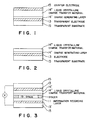
- image display devices when a device comprising a transparent substrate, such as glass, a transparent electrode, such as ITO (indium-tin-oxide), a charge generating layer capable of generating carriers according to exposure, the liquid crystalline charge transport material of the present invention, and a counter electrode (such as a gold electrode) laminated in that order is subjected to imagewise exposure (input image) through the bottom of the device as shown in the schematic diagram, the liquid crystalline charge transport material is aligned according to the exposure, resulting in flow of carriers in the counter electrode (gold electrode).
- the input image can be reproduced by optical reading of the alignment of the liquid crystal. The larger the smectic properties of the liquid crystal, the longer the storage time of the alignment of the liquid crystal and the longer the storage time of the input information.
- Figs. 1 to 3 are explanatory diagrams of embodiments where the liquid crystalline charge transport material according to the present invention has been applied to a charge transport layer in an image recording device.
- Fig. 1 is a schematic view of a photosensor, an embodiment where the liquid crystalline charge transport material according to the present invention has been applied to a charge transport layer. Use of the photosensor will be described in more detail.
- the device is subjected to pattern exposure from the direction of the above in the drawing while applying a voltage across the upper and lower electrodes 15. Carriers are generated in a pattern form in 14', and charges transported by a charge transport layer 14'' are discharged in a space 19 and reach the surface of an information recording layer 11.
- the information recording layer is, for example, a liquid crystal/polymer composite layer formed of a composite of a smectic liquid crystal and a polymer.
- the liquid crystal is aligned in a pattern form in an electric field of accumulated charges and accumulated, enabling optical recording to be performed.
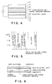
- exposure with a voltage being applied may be carried out in the same manner as described above in connection with the embodiment shown in Fig. 3.
- the generated charges (image) are accumulated on the top surface of a dielectric layer 20, and the liquid crystal is aligned in a pattern form in an electric field of charges accumulated in the same manner as described above in connection with the embodiment shown in Fig. 3 and accumulated, enabling optical reading to be performed.
- liquid crystalline charge transport material according to the present invention can be used also in a pace optical light modulating device schematically shown in Fig. 5.
- the liquid crystalline charge transport materials of the present invention can also be used as an active layer of a thin film transistor.
- the liquid crystalline material may be disposed on a substrate having thereon source, drain, and gate electrodes.
- liquid crystalline charge transport materials according to the present invention are useful for various applications such as photosensors, electroluminescence devices, photoconductors, space modulating devices, and thin film transistors.
- a 60 % by weight dispersion of 0.8 g (0.02 mol) of sodium hydride in an oil was suspended in 50 ml of ether, 3.22 g (0.022 mol) of 1-octanethiol was dropwise added thereto, and the mixture was refluxed for 30 min. Thereafter, the ether was distilled off, 50 ml of N,N-dimethylimidazolidinone was added to the residue, and the temperature of the system was raised to 60°C. 0.01 mol of 2-(4'-cyanophenyl)-6-bromobenzothiazole was added to the solution, and stirring was continued for one hr.
- Example A1 The procedure of Example A1 was repeated to prepare liquid crystalline compounds represented by the general formula (A) wherein R 1 and R 2 represent the following groups.
- the liquid crystalline compounds thus obtained had the same properties as the liquid crystalline compound prepared in Example A1.
- Example R 1 R 2 A5-1 CH 3 (CH 2 ) 9 O CN A5-2 CH 3 CH 2 C*H(CH 3 )CH 2 O CN A5-3 CH 3 (CH 2 ) 5 O O(CH 2 ) 9 CH 3 A5-4 NO 2 S(CH 2 ) 7 CH 3 A5-5 NO 2 O(CH 2 ) 7 CH 3 A5-6 F O(CH 2 ) 9 CH 3
- Example A2 The procedure of Example A2 was repeated to prepare liquid crystalline compounds represented by the general formula (B) wherein R 1 and R 2 represent the following groups.
- the liquid crystalline compounds thus obtained had the same properties as the liquid crystalline compound prepared in Example A2.
- Example A3 The procedure of Example A3 was repeated to prepare liquid crystalline compounds represented by the general formula (C) wherein R 1 represents the following groups.
- the liquid crystalline compounds thus obtained had the same properties as the liquid crystalline compound prepared in Example A3.
- Example R 1 A7-1 CH 3 (CH 2 ) 9 O A7-2 CH 3 (CH 2 ) 9 A7-3 CH 3 (CH 2 ) 9 S A7-4 CH 3 (CH 2 ) 5 S A7-5 CH 3 (CH 2 ) 8 S A7-6 CH 3 CH 2 C*H(CH 3 )CH 2 O
- Example A3 The procedure of Example A3 was repeated to prepare liquid crystalline compounds represented by the general formula (D) wherein R 1 represents the following group.
- the liquid crystalline compounds thus obtained had the same properties as the liquid crystalline compound prepared in Example A4.
- Example R 1 Z A8-1 CH 3 (CH 2 ) 5 O COO
- CH N A8-5 CH 3 (CH 2 ) 3 O
- N N A8-6 CH 3 (CH 2 ) 9 O COO
- novel liquid crystalline compounds which exhibit liquid crystallinity and, in addition, photoconductivity and fluorescence.
- the novel liquid crystalline compounds are useful as materials for liquid crystal displays, photosensitive materials for electrophotography and the like.
- Liquid crystalline compounds represented by the above general formula wherein R and R' represent the following groups were prepared in the same manner as in the above examples and comparative examples. All the liquid crystalline compounds thus obtained had the same properties as those prepared in Examples C1 to C4.
- Example R R' Example C5 Hexyl group Heptyl group
- Example C6 Octyl group Nonyl group
- Example C7 Hexyl group Undecynyl group
- novel liquid crystalline compounds which exhibit liquid crystallinity and, in addition, photoconductivity and fluorescence.
- novel liquid crystalline compounds are useful as materials for liquid crystal displays, photosensitive materials for electrophotography and the like.
Landscapes
- Chemical & Material Sciences (AREA)
- Organic Chemistry (AREA)
- Engineering & Computer Science (AREA)
- Materials Engineering (AREA)
- Crystallography & Structural Chemistry (AREA)
- Plural Heterocyclic Compounds (AREA)
- Liquid Crystal Substances (AREA)
- Organic Low-Molecular-Weight Compounds And Preparation Thereof (AREA)
- Heterocyclic Carbon Compounds Containing A Hetero Ring Having Nitrogen And Oxygen As The Only Ring Hetero Atoms (AREA)
Applications Claiming Priority (12)
| Application Number | Priority Date | Filing Date | Title |
|---|---|---|---|
| JP23903795A JP3839505B2 (ja) | 1995-08-25 | 1995-08-25 | 液晶性化合物 |
| JP239038/95 | 1995-08-25 | ||
| JP239037/95 | 1995-08-25 | ||
| JP23903795 | 1995-08-25 | ||
| JP23903895 | 1995-08-25 | ||
| JP23903895A JP3839506B2 (ja) | 1995-08-25 | 1995-08-25 | 液晶性化合物の製造方法 |
| JP9304596 | 1996-03-25 | ||
| JP09304596A JP3908298B2 (ja) | 1996-03-25 | 1996-03-25 | 液晶性化合物の製造方法 |
| JP9304496 | 1996-03-25 | ||
| JP93044/96 | 1996-03-25 | ||
| JP93045/96 | 1996-03-25 | ||
| JP9304496 | 1996-03-25 |
Publications (3)
| Publication Number | Publication Date |
|---|---|
| EP0763532A2 true EP0763532A2 (de) | 1997-03-19 |
| EP0763532A3 EP0763532A3 (de) | 2001-05-02 |
| EP0763532B1 EP0763532B1 (de) | 2004-08-11 |
Family
ID=27468105
Family Applications (1)
| Application Number | Title | Priority Date | Filing Date |
|---|---|---|---|
| EP96113638A Expired - Lifetime EP0763532B1 (de) | 1995-08-25 | 1996-08-26 | Flüssigkristalline Verbindung und deren Verwendung |
Country Status (3)
| Country | Link |
|---|---|
| US (2) | US5766510A (de) |
| EP (1) | EP0763532B1 (de) |
| DE (1) | DE69633098T2 (de) |
Cited By (8)
| Publication number | Priority date | Publication date | Assignee | Title |
|---|---|---|---|---|
| EP0915144A1 (de) * | 1997-11-04 | 1999-05-12 | Dai Nippon Printing Co., Ltd. | Fluoreszent flüssigkristall Ladungstransportmaterial |
| EP0864631A3 (de) * | 1997-03-10 | 1999-10-27 | Dai Nippon Printing Co., Ltd. | Flüssigkristall Ladungstransportmaterial |
| EP0972817A1 (de) * | 1998-07-13 | 2000-01-19 | Dai Nippon Printing Co., Ltd. | Ferroelektrisches flüssigkristallines Ladungstransportmaterial |
| EP1213336A3 (de) * | 2000-12-06 | 2002-09-04 | Sumitomo Chemical Company, Limited | Fluoreszierende polymer substanz und verwendung derselben in licht-emittierender vorrichtung |
| EP1104036A3 (de) * | 1999-11-29 | 2005-05-04 | Canon Kabushiki Kaisha | Flüssigkristallanordnung |
| JP2009057360A (ja) * | 2007-09-02 | 2009-03-19 | Junichi Hanna | ネマティック液晶性有機半導体材料 |
| US7550181B2 (en) | 1999-01-08 | 2009-06-23 | Dai Nippon Printing Co., Ltd. | Information recording medium |
| CN103396379A (zh) * | 2013-07-11 | 2013-11-20 | 华南理工大学 | 5,6-二氟苯并噻唑及其制备方法 |
Families Citing this family (9)
| Publication number | Priority date | Publication date | Assignee | Title |
|---|---|---|---|---|
| US5766510A (en) * | 1995-08-25 | 1998-06-16 | Dai Nippon Printing Co., Ltd. | Liquid crystalline compound and use thereof |
| US6720039B1 (en) | 1997-02-19 | 2004-04-13 | Dai Nippon Printing Co., Ltd. | Liquid crystalline compounds and process for producing the same |
| JP4262834B2 (ja) | 1999-06-14 | 2009-05-13 | 大日本印刷株式会社 | バインダー添加型電荷輸送液晶材料 |
| US6858271B1 (en) * | 1999-09-09 | 2005-02-22 | Canon Kabushiki Kaisha | Conductive organic compound device, conductive liquid crystal device, and organic electroluminescence device |
| JP3825969B2 (ja) | 1999-11-29 | 2006-09-27 | キヤノン株式会社 | 導電素子およびその製造方法 |
| JP2003068469A (ja) * | 2000-08-11 | 2003-03-07 | Canon Inc | 有機エレクトロルミネッセンス素子とその製造方法 |
| US7102154B2 (en) * | 2002-02-08 | 2006-09-05 | Dai Nippon Printing Co. Ltd | Organic semiconductor structure, process for producing the same, and organic semiconductor device |
| JP4870949B2 (ja) * | 2004-12-07 | 2012-02-08 | 日本化学工業株式会社 | 導電性材料、その製造方法、液晶組成物、半導体素子及び情報記録媒体 |
| EP1937616B1 (de) | 2005-10-21 | 2014-12-17 | LG Chem, Ltd. | Neue binaphthalinderivate, verfahren zu deren herstellung und organisches elektronisches gerät, bei dem diese verwendet werden |
Family Cites Families (17)
| Publication number | Priority date | Publication date | Assignee | Title |
|---|---|---|---|---|
| DE3528032A1 (de) * | 1985-08-05 | 1987-02-05 | Hoechst Ag | Verfahren zur herstellung 2-substituierter benzthiazole |
| US4861897A (en) * | 1987-06-22 | 1989-08-29 | Ortho Pharmaceutical Corporation | 2-Aryloxyalkylaminobenzoxazoles and 2-aryloxyalkylaminobenzothiazoles |
| US4803241A (en) * | 1987-07-20 | 1989-02-07 | Eastman Kodak Company | Condensation polymers containing styrylbenzazole ultraviolet radiation-absorbing residues and shaped articles produced therefrom |
| JPH01316386A (ja) * | 1988-03-22 | 1989-12-21 | Agency Of Ind Science & Technol | 2,6−(4,4’−ジアミノージフェニル)ベンゾ〔1,2−d:4,5−d’〕ビスチアゾールの製造方法 |
| GB8823721D0 (en) * | 1988-10-10 | 1988-11-16 | Boden N | Electronically conducting liquid crystals |
| JP2952053B2 (ja) * | 1991-01-30 | 1999-09-20 | キヤノン株式会社 | 光学活性化合物、これを含む液晶組成物、およびその使用方法、それを使用した液晶素子、表示装置 |
| JP2941971B2 (ja) * | 1991-02-13 | 1999-08-30 | キヤノン株式会社 | 液晶組成物、それを有する液晶素子、それ等を用いた表示方法及び表示装置 |
| JP2941972B2 (ja) * | 1991-02-14 | 1999-08-30 | キヤノン株式会社 | 液晶組成物、それを有する液晶素子、それ等を用いた表示方法及び表示装置 |
| JPH04290885A (ja) * | 1991-03-19 | 1992-10-15 | Mitsubishi Kasei Corp | 2,6−(4,4′−ジアミノ−ジフェニル)ベンゾ〔1,2−d:4,5−d′〕ビスチアゾールの製造方法 |
| JPH05125076A (ja) * | 1991-11-06 | 1993-05-21 | Canon Inc | 液晶性化合物、これを含む液晶組成物、それを有する液晶素子、それらを用いた表示方法及び表示装置 |
| DE69225685T2 (de) * | 1991-11-22 | 1998-11-26 | Canon K.K., Tokio/Tokyo | Flüssigkristallzusammensetzung, Flüssigkristallvorrichtung und Anzeigevorrichtung |
| DE4227029A1 (de) * | 1992-08-14 | 1994-02-17 | Basf Ag | Verfahren zur Herstellung von 2-(4'-Aminophenyl)-benzthiazolverbindungen |
| JP2537476B2 (ja) * | 1993-09-01 | 1996-09-25 | 株式会社同仁化学研究所 | ベンゾ− 1,3−チアゾ―ル骨格を有する蛍光ラベル化剤 |
| DE4336447A1 (de) * | 1993-10-26 | 1995-04-27 | Hoechst Ag | 6-Fluorbenzthiazole und ihre Verwendung in Flüssigkristallmischungen |
| DE4422332A1 (de) * | 1994-06-27 | 1996-01-04 | Basf Ag | Oligomere flüssigkristalline Triphenylenderivate und ihre Verwendung als Ladungstransportsubstanzen in der Elektrophotographie |
| DE4429597A1 (de) * | 1994-08-20 | 1996-02-22 | Basf Ag | Verwendung von in der kolumnar helicalen Phase vorliegenden niedermolekularen oder polymeren organischen Verbindungen mit flüssigkristallinen Eigenschaften |
| US5766510A (en) * | 1995-08-25 | 1998-06-16 | Dai Nippon Printing Co., Ltd. | Liquid crystalline compound and use thereof |
-
1996
- 1996-08-22 US US08/701,436 patent/US5766510A/en not_active Expired - Fee Related
- 1996-08-26 EP EP96113638A patent/EP0763532B1/de not_active Expired - Lifetime
- 1996-08-26 DE DE69633098T patent/DE69633098T2/de not_active Expired - Fee Related
-
1998
- 1998-04-03 US US09/054,500 patent/US5980779A/en not_active Expired - Lifetime
Cited By (11)
| Publication number | Priority date | Publication date | Assignee | Title |
|---|---|---|---|---|
| EP0864631A3 (de) * | 1997-03-10 | 1999-10-27 | Dai Nippon Printing Co., Ltd. | Flüssigkristall Ladungstransportmaterial |
| US6224787B1 (en) | 1997-03-10 | 2001-05-01 | Dai Nippon Printing Co., Ltd. | Liquid crystalline charge transport material |
| EP0915144A1 (de) * | 1997-11-04 | 1999-05-12 | Dai Nippon Printing Co., Ltd. | Fluoreszent flüssigkristall Ladungstransportmaterial |
| EP0972817A1 (de) * | 1998-07-13 | 2000-01-19 | Dai Nippon Printing Co., Ltd. | Ferroelektrisches flüssigkristallines Ladungstransportmaterial |
| US6218061B1 (en) | 1998-07-13 | 2001-04-17 | Dai Nippon Printing Co., Ltd. | Ferroelectric charge-transport liquid crystal material |
| US7550181B2 (en) | 1999-01-08 | 2009-06-23 | Dai Nippon Printing Co., Ltd. | Information recording medium |
| EP1104036A3 (de) * | 1999-11-29 | 2005-05-04 | Canon Kabushiki Kaisha | Flüssigkristallanordnung |
| EP1213336A3 (de) * | 2000-12-06 | 2002-09-04 | Sumitomo Chemical Company, Limited | Fluoreszierende polymer substanz und verwendung derselben in licht-emittierender vorrichtung |
| US7701129B2 (en) | 2000-12-06 | 2010-04-20 | Sumitomo Chemical Company, Limited | Polymeric fluorescent substance and polymer light-emitting device using the same |
| JP2009057360A (ja) * | 2007-09-02 | 2009-03-19 | Junichi Hanna | ネマティック液晶性有機半導体材料 |
| CN103396379A (zh) * | 2013-07-11 | 2013-11-20 | 华南理工大学 | 5,6-二氟苯并噻唑及其制备方法 |
Also Published As
| Publication number | Publication date |
|---|---|
| DE69633098T2 (de) | 2005-08-11 |
| EP0763532A3 (de) | 2001-05-02 |
| US5980779A (en) | 1999-11-09 |
| US5766510A (en) | 1998-06-16 |
| EP0763532B1 (de) | 2004-08-11 |
| DE69633098D1 (de) | 2004-09-16 |
Similar Documents
| Publication | Publication Date | Title |
|---|---|---|
| EP0763532B1 (de) | Flüssigkristalline Verbindung und deren Verwendung | |
| Hsung et al. | Synthesis and Characterization of Unsymmetric Ferrocene-Terminated Phenylethynyl Oligomers Cp2Fe-[C. tplbond. C-C6H4] nX,(X= SH, SMe, SOMe, and SO2Me) | |
| US5723671A (en) | Arylamine processes | |
| EP2166001A1 (de) | Carbazolderivat und Herstellungsverfahren dafür | |
| JP2001515120A (ja) | 対になったred−ox系および特定アニオンを有するエレクトロクロミック系 | |
| Li et al. | Synthesis and characterization of triphenylethylene derivatives with aggregation-induced emission characteristics | |
| JP2013056878A (ja) | キラルドーパント、それを用いた液晶混合物および液晶ディスプレイ | |
| JP4116109B2 (ja) | エレクトロルミネッセンス素子用組成物 | |
| EP0592366A1 (de) | Photochrome Verbindungen, deren Herstellung und deren Verwendung | |
| JP3262313B2 (ja) | 電荷輸送化合物の製造方法及び得られた電荷輸送化合物を含有する電子写真感光体 | |
| JP4527662B2 (ja) | 長い直線的共役系構造部分を持つベンゼン誘導体、その製造方法及び液晶性材料 | |
| JP4343516B2 (ja) | 有機半導体材料と有機半導体素子の製造方法 | |
| JP4476933B2 (ja) | 長い直線的共役系構造部分を持つベンゼン誘導体、その製造方法、液晶性材料及び電荷輸送材料 | |
| CN119874574B (zh) | 一种三芳基乙烯固体光致变色染料及其晶体制备 | |
| JPH0481998B2 (de) | ||
| JP4697367B2 (ja) | ジヒドロピレン誘導体 | |
| CN119409658B (zh) | 用于制备电致变色器件阳极材料的吩噁嗪衍生物、其制备方法、阳极材料和电致变色介质组合物 | |
| JPH08337548A (ja) | トリフェニレン誘導体 | |
| KR19990088680A (ko) | 트리페노디옥사진화합물,그의제조방법,2색성색소로서의용도및액정조성물 | |
| JP3358017B2 (ja) | トリスアゾ化合物 | |
| JP2001011070A (ja) | カルコゲノピリリウム化合物の製造方法 | |
| JP3839505B2 (ja) | 液晶性化合物 | |
| US20050064130A1 (en) | Nonlinear optical element, electro-optic element, and compound | |
| JP4574549B2 (ja) | 長い直線的共役系構造部分を持つベンゼン誘導体、その製造方法及び液晶性材料 | |
| JP3839506B2 (ja) | 液晶性化合物の製造方法 |
Legal Events
| Date | Code | Title | Description |
|---|---|---|---|
| PUAI | Public reference made under article 153(3) epc to a published international application that has entered the european phase |
Free format text: ORIGINAL CODE: 0009012 |
|
| AK | Designated contracting states |
Kind code of ref document: A2 Designated state(s): DE FR GB |
|
| RIC1 | Information provided on ipc code assigned before grant |
Free format text: 7C 07D 277/66 A, 7C 09K 19/34 B, 7G 02F 1/13 B, 7C 09K 11/06 B, 7G 11C 13/04 B |
|
| PUAL | Search report despatched |
Free format text: ORIGINAL CODE: 0009013 |
|
| AK | Designated contracting states |
Kind code of ref document: A3 Designated state(s): DE FR GB |
|
| RIC1 | Information provided on ipc code assigned before grant |
Free format text: 7C 07D 277/66 A, 7C 09K 19/34 B, 7G 02F 1/13 B, 7C 09K 11/06 B, 7G 11C 13/04 B, 7C 09K 19/02 B |
|
| 17P | Request for examination filed |
Effective date: 20010628 |
|
| 17Q | First examination report despatched |
Effective date: 20020228 |
|
| GRAP | Despatch of communication of intention to grant a patent |
Free format text: ORIGINAL CODE: EPIDOSNIGR1 |
|
| GRAS | Grant fee paid |
Free format text: ORIGINAL CODE: EPIDOSNIGR3 |
|
| GRAA | (expected) grant |
Free format text: ORIGINAL CODE: 0009210 |
|
| AK | Designated contracting states |
Kind code of ref document: B1 Designated state(s): DE FR GB |
|
| REG | Reference to a national code |
Ref country code: GB Ref legal event code: FG4D |
|
| REF | Corresponds to: |
Ref document number: 69633098 Country of ref document: DE Date of ref document: 20040916 Kind code of ref document: P |
|
| ET | Fr: translation filed | ||
| PLBE | No opposition filed within time limit |
Free format text: ORIGINAL CODE: 0009261 |
|
| STAA | Information on the status of an ep patent application or granted ep patent |
Free format text: STATUS: NO OPPOSITION FILED WITHIN TIME LIMIT |
|
| 26N | No opposition filed |
Effective date: 20050512 |
|
| PGFP | Annual fee paid to national office [announced via postgrant information from national office to epo] |
Ref country code: DE Payment date: 20080828 Year of fee payment: 13 |
|
| PGFP | Annual fee paid to national office [announced via postgrant information from national office to epo] |
Ref country code: FR Payment date: 20080806 Year of fee payment: 13 |
|
| PGFP | Annual fee paid to national office [announced via postgrant information from national office to epo] |
Ref country code: GB Payment date: 20080827 Year of fee payment: 13 |
|
| GBPC | Gb: european patent ceased through non-payment of renewal fee |
Effective date: 20090826 |
|
| REG | Reference to a national code |
Ref country code: FR Ref legal event code: ST Effective date: 20100430 |
|
| PG25 | Lapsed in a contracting state [announced via postgrant information from national office to epo] |
Ref country code: FR Free format text: LAPSE BECAUSE OF NON-PAYMENT OF DUE FEES Effective date: 20090831 Ref country code: DE Free format text: LAPSE BECAUSE OF NON-PAYMENT OF DUE FEES Effective date: 20100302 |
|
| PG25 | Lapsed in a contracting state [announced via postgrant information from national office to epo] |
Ref country code: GB Free format text: LAPSE BECAUSE OF NON-PAYMENT OF DUE FEES Effective date: 20090826 |