EP0763878A2 - Alimentation à faible énergie pour la commande à phase hors-ligne - Google Patents
Alimentation à faible énergie pour la commande à phase hors-ligne Download PDFInfo
- Publication number
- EP0763878A2 EP0763878A2 EP96114117A EP96114117A EP0763878A2 EP 0763878 A2 EP0763878 A2 EP 0763878A2 EP 96114117 A EP96114117 A EP 96114117A EP 96114117 A EP96114117 A EP 96114117A EP 0763878 A2 EP0763878 A2 EP 0763878A2
- Authority
- EP
- European Patent Office
- Prior art keywords
- power supply
- coupled
- voltage
- source
- transistor
- Prior art date
- Legal status (The legal status is an assumption and is not a legal conclusion. Google has not performed a legal analysis and makes no representation as to the accuracy of the status listed.)
- Withdrawn
Links
Images


Classifications
-
- H—ELECTRICITY
- H02—GENERATION; CONVERSION OR DISTRIBUTION OF ELECTRIC POWER
- H02M—APPARATUS FOR CONVERSION BETWEEN AC AND AC, BETWEEN AC AND DC, OR BETWEEN DC AND DC, AND FOR USE WITH MAINS OR SIMILAR POWER SUPPLY SYSTEMS; CONVERSION OF DC OR AC INPUT POWER INTO SURGE OUTPUT POWER; CONTROL OR REGULATION THEREOF
- H02M7/00—Conversion of AC power input into DC power output; Conversion of DC power input into AC power output
- H02M7/02—Conversion of AC power input into DC power output without possibility of reversal
- H02M7/04—Conversion of AC power input into DC power output without possibility of reversal by static converters
- H02M7/12—Conversion of AC power input into DC power output without possibility of reversal by static converters using discharge tubes with control electrode or semiconductor devices with control electrode
- H02M7/21—Conversion of AC power input into DC power output without possibility of reversal by static converters using discharge tubes with control electrode or semiconductor devices with control electrode using devices of a triode or transistor type requiring continuous application of a control signal
- H02M7/217—Conversion of AC power input into DC power output without possibility of reversal by static converters using discharge tubes with control electrode or semiconductor devices with control electrode using devices of a triode or transistor type requiring continuous application of a control signal using semiconductor devices only
- H02M7/2176—Conversion of AC power input into DC power output without possibility of reversal by static converters using discharge tubes with control electrode or semiconductor devices with control electrode using devices of a triode or transistor type requiring continuous application of a control signal using semiconductor devices only comprising a passive stage to generate a rectified sinusoidal voltage and a controlled switching element in series between such stage and the output
-
- H—ELECTRICITY
- H04—ELECTRIC COMMUNICATION TECHNIQUE
- H04N—PICTORIAL COMMUNICATION, e.g. TELEVISION
- H04N5/00—Details of television systems
- H04N5/63—Generation or supply of power specially adapted for television receivers
Definitions
- This invention relates generally to the field of power supplies, and in particular, to standby power supplies used, for example, in television receivers.
- a television receiver may be designed such that the television receiver's functions can be controlled by a viewer from a remote location using a hand-held, remote control apparatus.
- the television receiver includes a standby power supply, which supplies power to the television receiver's microprocessor and to certain of its signal processing circuitry while the television receiver is in the "off" state.
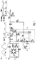
- FIGURE 3 shows a schematic diagram of a typical prior art standby power supply which uses a linear regulator circuit.
- a source of AC input voltage is full-wave rectified by diodes D1, D2, D3 and D4 to provide a rectified voltage V REC .
- Rectified voltage V REC is filtered by capacitor C5.
- Transistor Q6 forms a series pass element which receives rectified voltage V REC and provides an output voltage V OUT .
- the conductivity of series pass element Q6 is adjusted so as to maintain a relatively constant output voltage V OUT .
- a disadvantage associated with the linear regulator circuit concerns the power dissipated as heat in series pass element Q6.
- Energy stored in capacitor C5 does not allow rectified voltage V REC to drop below output voltage V OUT , and thereby prevents series pass element Q6 from turning "off".
- Series pass element Q6 operates in its linear region, and thus may have a substantial voltage drop from its input to its output.
- An output current flows through series pass element Q6 during the entire cycle of the AC input voltage. This combination of an output current flowing through a potentially sizable voltage drop may lead to high power dissipation in series pass element Q6.
- a large power dissipation in series pass element Q6 is undesirable for at least two reasons.
- Circuits employing phase control techniques can be used to overcome the drawbacks associated with the linear regulator circuit by controlling the amount of power delivered to a load.
- a silicon-controlled rectifier SCR
- the SCR's gate electrode is usually triggered through a diac to ensure that the SCR does not conduct prematurely. If conduction is desired during a portion of both the positive and the negative half-cycles of AC input voltage, a triac can be used in place of the SCR.
- a drawback to implementing phase control techniques using SCRs and triacs is that such an approach can result in high peak output currents.
- the use of a silicon-controlled rectifier permits only one current pulse during each cycle of AC input voltage; the use of a triac permits only two current pulses during each cycle of AC input voltage.
- a power supply according to the inventive arrangements taught herein results in lower peak output currents and more current pulses during each cycle of AC input voltage than are currently associated with power supplies employing phase control techniques.
- Such a power supply comprises: a source of unfiltered, rectified voltage potential; switching means coupled to the source for providing a regulated output voltage; means for generating a reference voltage potential coupled to the source; and, means for controlling operation of the switching means coupled to the generating means.
- the switching means may conduct only after the rectified voltage potential falls below a threshold level, and the switching means may stop conducting after the rectified voltage potential rises above the threshold level.
- the power supply may further comprise feedback means coupled from an output of the power supply to the generating means.
- the feedback means may comprise a resistance.
- the power supply may provide four current pulses during each cycle of an alternating voltage potential.
- a power supply comprises: a source of rectified voltage potential; switching means which changes between non-conducting and fully conducting states responsive to the source of rectified voltage potential; means for generating a reference voltage potential coupled to the source; and, feedback means coupled from an output of the power supply to the generating means.
- the power supply may provide four current pulses during each cycle of an alternating voltage potential.
- the feedback means may comprise a resistance.
- a peak amplitude of the current pulses may be responsive to the resistance.
- a threshold level for the rectified voltage potential may be responsive to the resistance.
- the switching means may be in a non-conducting state when the rectified input voltage is above the threshold level.
- the switching means may be in a fully conducting state when the rectified input voltage is below the threshold level.
- FIGURE 1 is a schematic diagram of a preferred embodiment of an inventive arrangement taught herein.
- FIGURE 2 is a schematic diagram of another preferred embodiment of an inventive arrangement taught herein.
- FIGURE 3 is a schematic diagram of a prior art standby power supply.
- Power supplies 10 and 10' are shown in FIGURES 1 and 2, respectively. Each power supply accepts an AC voltage potential V AC from a source of alternating voltage potential 11.
- the AC voltage potential V AC typically has a peak voltage V PK between 30 volts and 270 volts and operates at a frequency greater than or equal to about 50 Hz.
- Power supply 10 provides a DC output power at an output voltage V OUT , for example between 15 and 17 volts, and a nominal output current I OUT , for example up to 60 mA.
- source of alternating voltage potential 11 has a first terminal coupled to an anode of diode D5 and a second terminal coupled to an anode of diode D6.
- the cathodes of diodes D5 and D6 are coupled to one another.
- the AC voltage potential V AC is full-wave rectified by diodes D5 and D6 to provide a rectified voltage V REC at the cathodes of diodes D5 and D6.
- Rectified voltage V REC is not filtered by an input filter.
- a switch device Q1 may comprise, for example, an enhancement-type, n-channel, metal-oxide semiconductor field-effect transistor (MOSFET).
- MOSFET metal-oxide semiconductor field-effect transistor
- a resistor R1 has a first terminal coupled to the cathodes of diodes D5 and D6 and a second terminal coupled to a drain electrode of switch device Q1.
- a voltage regulator VR2 has a cathode coupled to a gate electrode of switch device Q1 and an anode coupled to a source electrode of switch device Q1.
- Voltage regulator VR2 is, for example, a Zener diode having a reverse breakdown voltage equal to 9.1 volts.
- the source electrode of switch device Q1 is also coupled to an anode of a diode D8.
- a control circuit 12 for switch device Q1 may generally comprise resistors R2, R3 and R7, and a transistor Q2.
- a first terminal of resistor R2 is coupled to the gate electrode of switch device Q1.
- a first terminal of resistor R3 is coupled to the cathodes of diodes D5 and D6, and a second terminal of resistor R3 is coupled to a second terminal of resistor R2.
- the second terminals of resistors R2 and R3 are coupled to a collector electrode of transistor Q2.
- An emitter electrode of transistor Q2 is coupled to a source of power supply reference potential, for example, ground.
- a base electrode of transistor Q2 is coupled to a first terminal of resistor R7, and a second terminal of resistor R7 is coupled to the source of power supply reference potential.
- a reference voltage circuit 13 may generally comprise a reference voltage regulator VR1 and resistors R4 and R5.
- Reference voltage regulator VR1 is, for example, a Zener diode having a reverse breakdown voltage equal to 15 volts.
- An anode of reference voltage regulator VR1 is coupled to the base electrode of transistor Q2.
- a cathode of reference voltage regulator VR1 is coupled to a first terminal of resistor R5.
- a second terminal of resistor R5 is coupled to the source of power supply reference potential.
- a resistor R4 has a first terminal coupled to the cathode of reference voltage regulator VR1 and a second terminal coupled to the cathodes of diodes D5 and D6.
- Resistor R6 couples reference voltage V REF at the cathode of reference voltage regulator VR1 to output voltage V OUT at a cathode of diode D8.
- a capacitor C2 has a first terminal coupled to a cathode of diode D8 and a second terminal coupled to the source of power supply reference potential.
- a voltage divider network formed by resistors R4 and R5 divides rectified voltage V REC such that the voltage at the cathode of reference voltage regulator VR1 is approximately equal to V REC *( R5 R4+R5 ).
- power supply 10 has a closed-loop configuration, that is, resistor R6 couples reference voltage V REF at the cathode of reference voltage regulator VR1 to output voltage V OUT at a cathode of diode D8.
- the output voltage V OUT at the cathode of diode D8 is equal to the sum of the reverse breakdown voltage across reference voltage regulator VR1, the voltage between the base and emitter electrodes of transistor Q2 and a ripple voltage component V RIPPLE.
- the ripple voltage component V RIPPLE of output voltage V OUT arises from the periodic charging and discharging of capacitor C2.
- Ripple voltage V RIPPLE reaches a positive peak value of approximately 0.5 volts during the time that output current I OUT is charging capacitor C2.
- ripple voltage V RIPPLE reaches a negative peak value of approximately -0.5 volts during the time that switch device Q1 is not conducting output current I OUT and capacitor C2 is discharging into a load.
- reference voltage V REF maintains a value that is substantially equal to the reverse breakdown voltage of reference voltage regulator VR1 plus the voltage between the base and emitter electrodes of transistor Q2. Therefore, a current I R4 through resistor R4 decreases.
- Switch device Q1 continues conducting output current I OUT until rectified voltage V REC decreases below the level of output voltage V OUT .
- Output voltage V OUT is coupled to the drain electrode of switch device Q1 through resistors R1, R4 and R6.
- a drain voltage V D becomes approximately equal to the output voltage V OUT .
- switch device Q1 temporarily discontinues conducting output current I OUT , thereby minimizing power dissipation in resistor R1.
- reference voltage regulator VR1 When rectified voltage V REC again reaches the threshold level, the reverse breakdown voltage of reference voltage regulator VR1 is exceeded and reference voltage regulator VR1 maintains a substantially constant voltage drop of 15 volts from its cathode to its anode.
- Current I Z flows through reference voltage regulator VR1 and into the base electrode of transistor Q2, causing transistor Q2 to become conductive, and thereby pulling the gate electrode of switch device Q1 to the source of power supply reference potential through resistor R2 of control circuit 12 and causing switch device Q1 to become non-conductive.
- This process repeats itself for each cycle of AC voltage potential V AC .
- Four current pulses are produced during each cycle of AC voltage potential V AC because transistor Q2 remains non-conductive throughout the time that rectified voltage V REC remains below the threshold level. This allows switch device Q1 to resume conducting output current I OUT once rectified voltage V REC exceeds the level of output voltage V OUT as rectified voltage V REC increases toward its peak voltage V PK .
- switch device Q1 can be operated without having to be mounted on a heat sink.
- the power dissipation associated with output current I OUT occurs primarily in resistor R1 because switch device Q1 is in a fully conductive state when it is conducting output current I OUT .
- Power supply 10' shown in FIGURE 2, is an alternative embodiment for power supply 10.
- a switch device Q3 may comprise, for example, a PNP-type, bipolar junction transistor (BJT). Switch device Q3 corresponds in function to switch device Q1 of FIGURE 1.
- BJT bipolar junction transistor
- the AC voltage potential V AC provided by source of alternating voltage potential 11 is full-wave rectified by diodes D1, D2, D3 and D4 to provide rectified voltage V REC at the cathodes of diodes D3 and D4.
- rectified voltage V REC is not filtered by an input filter.
- Diode D9 conducts when rectified voltage V REC exceeds a RAW B + voltage.
- Resistor R8 which corresponds in function to resistor R1 of FIGURE 1, has a first terminal coupled to the cathodes of diodes D3 and D4 and a second terminal coupled to an emitter electrode of switch device Q3.
- a collector electrode of switch device Q3 is coupled to the anode of diode D8, which performs the same function in both of the embodiments shown in FIGURES 1 and 2.
- a control circuit 14 for switch device Q3 may generally comprise resistors R9, R10 and R13, and transistors Q4 and Q5.
- Control circuit 14 corresponds in function to control circuit 12 of FIGURE 1.
- Transistor Q5 is necessary in control circuit 14 only because of the base current requirements of PNP-type BJTs.
- a first terminal of resistor R9 is coupled to a base electrode of switch device Q3.
- a first terminal of resistor R10 is coupled to the emitter electrode of switch device Q3, and a second terminal of resistor R10 is coupled to the first terminal of resistor R9.
- a second terminal of resistor R9 is coupled to a collector electrode of transistor Q4.
- An emitter electrode of transistor Q4 is coupled to a source of power supply reference potential, for example, ground.
- a collector electrode of transistor Q5 is coupled to a base electrode of transistor Q4.
- a base electrode of transistor Q5 is coupled to a first terminal of resistor R13.
- a second terminal of resistor R13 and an emitter electrode of transistor Q5 are coupled to the source of power supply reference potential.
- a reference voltage circuit 15, which corresponds in function to reference voltage circuit 13 of FIGURE 1, may generally comprise a reference voltage regulator VR3 and resistors R11 and R12.
- Reference voltage regulator VR3 is, for example, a Zener diode having a reverse breakdown voltage equal to 15 volts.
- An anode of reference voltage regulator VR3 is coupled to the base electrode of transistor Q5.
- a cathode of reference voltage regulator VR3 is coupled to a first terminal of resistor R12.
- a second terminal of resistor R12 is coupled to the collector electrode of transistor Q5.
- Resistor R11 has a first terminal coupled to the cathode of reference voltage regulator VR3 and a second terminal coupled to the cathodes of diodes D3 and D4.
- Resistor R14 which corresponds in function to resistor R6 of FIGURE 1, couples reference voltage V REF at the cathode of reference voltage regulator VR3 to output voltage V OUT at the cathode of diode D8.
- Capacitor C2 which performs the same function in both of the embodiments shown in FIGURES 1 and 2, has a first terminal coupled to a cathode of diode D8 and a second terminal coupled to the source of power supply reference potential.
- a voltage divider network formed by resistors R11 and R12 divides rectified voltage V REC such that the voltage at the cathode of reference voltage regulator VR3 is approximately equal to V REC *( R12 R11+R12 ).
- power supply 10' has a closed-loop configuration, that is, resistor R14 couples reference voltage V REF at the cathode of reference voltage regulator VR3 to output voltage V OUT at the cathode of diode D8.
- the output voltage V OUT at the cathode of diode D8 is equal to the sum of the reverse breakdown voltage across reference voltage regulator VR3, the voltage between the base and emitter electrodes of transistor Q5 and a ripple voltage component V RIPPLE .
- the ripple voltage component V RIPPLE of output voltage V OUT arises from the periodic charging and discharging of capacitor C2.
- Ripple voltage V RIPPLE reaches a positive peak value of approximately 0.5 volts during the time that output current I OUT is charging capacitor C2.
- ripple voltage V RIPPLE reaches a negative peak value of approximately -0.5 volts during the time that switch device Q3 is not conducting output current I OUT and capacitor C2 is discharging into a load.
- reference voltage V REF maintains a value that is substantially equal to the reverse breakdown voltage of reference voltage regulator VR3 plus the voltage between the base and emitter electrodes of transistor Q5. Therefore, a current I R11 through resistor R11 decreases.
- Switch device Q3 continues conducting output current I OUT until rectified voltage V REC decreases below the level of output voltage V OUT .
- rectified voltage V REC drops below output voltage V OUT , which is possible because of the absence of an input filter capacitor that would otherwise hold rectified voltage V REC up at a much higher level
- an emitter voltage V E becomes approximately equal to the sum of the voltage between the collector and emitter electrodes of transistor Q4 and the voltage between the emitter and base electrodes of switch device Q3.
- switch device Q3 temporarily discontinues conducting output current I OUT , thereby minimizing power dissipation in resistor R8.
- This process repeats itself for each cycle of the AC voltage potential V AC .
- Four current pulses are produced during each cycle of AC voltage potential V AC because transistor Q4 remains conductive throughout the time that rectified voltage V REC remains below the threshold level. This allows switch device Q3 to resume conducting output current I OUT once rectified voltage V REC exceeds the level of output voltage V OUT as rectified voltage V REC increases toward its peak voltage V PK .
- switch device Q3 can be operated without having to be mounted on a heat sink.
- the power dissipation associated with output current I OUT occurs primarily in resistor R8 because switch device Q3 is in a fully conductive state when it is conducting output current I OUT .
- a value for resistors R6 and R14 in FIGURES 1 and 2, respectively, can be chosen in order to achieve a desired threshold level for rectified voltage V REC .
- a particular threshold level may be desirable because of its effect on a peak amplitude I PK of output current I OUT .
- resistors R6 and R14 are each replaced by a short circuit, all power is delivered to the load by a single current pulse. This leads to more power being dissipated by each power supply because the single current pulse necessarily has a high peak amplitude.
- Adjusting the values of R6 and R14 allows the relative amplitudes of adjacent current pulses of output current I OUT to be approximately equalized so that the power dissipated by power supplies 10 and 10', respectively, may be minimized.
- current I Z through reference voltage regulators VR1 and VR3 in FIGURES 1 and 2, respectively reaches zero at a lower threshold level. This, in turn, causes switch devices Q1 and Q3 to begin conducting output current I OUT at a lower value of rectified voltage V REC than would be the case with lower values for resistors R6 and R14.
- a value for resistors R6 and R14 may thus be chosen such that the relative amplitudes of adjacent current pulses of output current I OUT may be approximately equalized.
- resistor R6 equal to 3.6 k ⁇
- the relative amplitudes of adjacent current pulses of output current I OUT are unequal.
- a first current pulse has a peak amplitude which is equal to the peak amplitude I PK of the output current I OUT , which is approximately equal to 0.75 A in FIGURE 1.
- a second, adjacent current pulse then has an amplitude that is less than the peak amplitude I PK of output current I OUT because power supply 10 provides a constant output power, and thus the second, adjacent current pulse need only supply whatever power was not supplied by the first current pulse.
- the second, adjacent current pulse has an amplitude which is approximately equal to 0.65 A.
- both adjacent current pulses of output current I OUT of power supply 10' have an amplitude which is approximately equal to the peak amplitude I PK of output current I OUT.
- both adjacent current pulses have an amplitude which is approximately equal to 0.7 A. As a result, each adjacent current pulse supplies a relatively equal amount of power to the load.
- a transistor switch device is driven between the non-conductive and fully conductive states by a control circuit comprising a plurality of resistors and at least one active device.
- the control circuits in each embodiment drive their respective switch devices into the fully conductive state once an unfiltered, full-wave rectified waveform drops below a threshold voltage level, which is set in each embodiment by a reference voltage circuit comprising a voltage divider network and a Zener diode.
- the switch device remains in the fully conductive state until the unfiltered, full-wave rectified voltage waveform exceeds the threshold level, at which point the control circuits in each embodiment drive their respective switch devices into the non-conductive state.
- the output voltage in each embodiment is determined by a resistive feedback connection from the power supply's output to its reference voltage circuit.
- the power supply provides four current pulses during each cycle of the source of alternating voltage potential.
- the peak amplitudes of the current pulses in each embodiment can be controlled by the selection of a resistance value for the feedback connection.
Landscapes
- Engineering & Computer Science (AREA)
- Multimedia (AREA)
- Signal Processing (AREA)
- Power Engineering (AREA)
- Dc-Dc Converters (AREA)
- Rectifiers (AREA)
- Control Of Electrical Variables (AREA)
- Power Conversion In General (AREA)
- Television Receiver Circuits (AREA)
Applications Claiming Priority (2)
| Application Number | Priority Date | Filing Date | Title |
|---|---|---|---|
| US52948195A | 1995-09-18 | 1995-09-18 | |
| US529481 | 1995-09-18 |
Publications (2)
| Publication Number | Publication Date |
|---|---|
| EP0763878A2 true EP0763878A2 (fr) | 1997-03-19 |
| EP0763878A3 EP0763878A3 (fr) | 1997-11-05 |
Family
ID=24110091
Family Applications (1)
| Application Number | Title | Priority Date | Filing Date |
|---|---|---|---|
| EP96114117A Withdrawn EP0763878A3 (fr) | 1995-09-18 | 1996-09-04 | Alimentation à faible énergie pour la commande à phase hors-ligne |
Country Status (7)
| Country | Link |
|---|---|
| EP (1) | EP0763878A3 (fr) |
| JP (1) | JPH09198150A (fr) |
| KR (1) | KR970019532A (fr) |
| CN (1) | CN1150351A (fr) |
| MX (1) | MX9604162A (fr) |
| SG (1) | SG44974A1 (fr) |
| TW (1) | TW332369B (fr) |
Cited By (7)
| Publication number | Priority date | Publication date | Assignee | Title |
|---|---|---|---|---|
| FR2787648A1 (fr) * | 1998-12-17 | 2000-06-23 | St Microelectronics Sa | Convertisseur d'une haute tension alternative en une basse tension continue |
| US6778416B2 (en) | 2001-08-10 | 2004-08-17 | Somfy Sas | Unregulated voltage converter with independent switching |
| US7075805B2 (en) | 2001-10-02 | 2006-07-11 | Somfy Sas | Voltage converter with current limiting portion |
| WO2009059646A1 (fr) * | 2007-11-09 | 2009-05-14 | Osram Gesellschaft mit beschränkter Haftung | Alimentation en tension auxiliaire pour un fonctionnement en mode de veille |
| WO2009132693A1 (fr) * | 2008-04-28 | 2009-11-05 | Inventio Ag | Procédé de commutation de consommateurs électriques dans un bâtiment |
| FR3101492A1 (fr) * | 2019-10-01 | 2021-04-02 | Schneider Electric Industries Sas | circuit de régulation en tension et module d’alimentation régulée |
| WO2021183172A1 (fr) | 2020-03-09 | 2021-09-16 | Intelesol, Llc | Convertisseur ca-cc |
Families Citing this family (3)
| Publication number | Priority date | Publication date | Assignee | Title |
|---|---|---|---|---|
| CN100389371C (zh) * | 2004-09-16 | 2008-05-21 | 中芯国际集成电路制造(上海)有限公司 | 具有低待机电流的调压器用器件和方法 |
| CN100416441C (zh) * | 2005-03-10 | 2008-09-03 | 崇贸科技股份有限公司 | 具有分流控制的稳压器与电源供应器 |
| CN100421044C (zh) * | 2005-03-10 | 2008-09-24 | 崇贸科技股份有限公司 | 分流装置及方法 |
Family Cites Families (3)
| Publication number | Priority date | Publication date | Assignee | Title |
|---|---|---|---|---|
| US4685046A (en) * | 1985-10-03 | 1987-08-04 | The Scott & Fetzer Company | Low voltage direct current power supply |
| DE3727117A1 (de) * | 1987-08-14 | 1989-02-23 | Diehl Gmbh & Co | Verfahren zur erzeugung einer niedrigen stabilisierten gleichspannung |
| JP3126565B2 (ja) * | 1993-11-01 | 2001-01-22 | 株式会社東芝 | Ac/dc変換器 |
-
1996
- 1996-08-30 TW TW085110569A patent/TW332369B/zh active
- 1996-09-04 EP EP96114117A patent/EP0763878A3/fr not_active Withdrawn
- 1996-09-12 KR KR1019960039454A patent/KR970019532A/ko not_active Withdrawn
- 1996-09-17 JP JP8245160A patent/JPH09198150A/ja active Pending
- 1996-09-17 CN CN96112926A patent/CN1150351A/zh active Pending
- 1996-09-17 SG SG1996010643A patent/SG44974A1/en unknown
- 1996-09-18 MX MX9604162A patent/MX9604162A/es unknown
Cited By (13)
| Publication number | Priority date | Publication date | Assignee | Title |
|---|---|---|---|---|
| FR2787648A1 (fr) * | 1998-12-17 | 2000-06-23 | St Microelectronics Sa | Convertisseur d'une haute tension alternative en une basse tension continue |
| EP1014551A1 (fr) * | 1998-12-17 | 2000-06-28 | STMicroelectronics S.A. | Convertisseur d'une haute tension alternative en une basse tension continue |
| US6246597B1 (en) | 1998-12-17 | 2001-06-12 | Stmicroelectronics S.A. | A.C./D.C. converter having a linearly controllable one-way switch, and using no high voltage passive components |
| US6778416B2 (en) | 2001-08-10 | 2004-08-17 | Somfy Sas | Unregulated voltage converter with independent switching |
| US6982888B2 (en) | 2001-08-10 | 2006-01-03 | Somfy Sas | Unregulated electrical converter |
| US7075805B2 (en) | 2001-10-02 | 2006-07-11 | Somfy Sas | Voltage converter with current limiting portion |
| WO2009059646A1 (fr) * | 2007-11-09 | 2009-05-14 | Osram Gesellschaft mit beschränkter Haftung | Alimentation en tension auxiliaire pour un fonctionnement en mode de veille |
| WO2009132693A1 (fr) * | 2008-04-28 | 2009-11-05 | Inventio Ag | Procédé de commutation de consommateurs électriques dans un bâtiment |
| FR3101492A1 (fr) * | 2019-10-01 | 2021-04-02 | Schneider Electric Industries Sas | circuit de régulation en tension et module d’alimentation régulée |
| EP3800775A1 (fr) * | 2019-10-01 | 2021-04-07 | Schneider Electric Industries SAS | Circuit de regulation en tension et module d'alimentation regulee |
| US11451148B2 (en) | 2019-10-01 | 2022-09-20 | Schneider Electric Industries Sas | Voltage-regulating circuit and regulated power-supply module |
| WO2021183172A1 (fr) | 2020-03-09 | 2021-09-16 | Intelesol, Llc | Convertisseur ca-cc |
| EP4118936A4 (fr) * | 2020-03-09 | 2024-04-03 | Intelesol, LLC | Convertisseur ca-cc |
Also Published As
| Publication number | Publication date |
|---|---|
| SG44974A1 (en) | 1997-12-19 |
| TW332369B (en) | 1998-05-21 |
| KR970019532A (ko) | 1997-04-30 |
| MX9604162A (es) | 1997-08-30 |
| CN1150351A (zh) | 1997-05-21 |
| JPH09198150A (ja) | 1997-07-31 |
| EP0763878A3 (fr) | 1997-11-05 |
Similar Documents
| Publication | Publication Date | Title |
|---|---|---|
| EP0651499B1 (fr) | Convertisseur de tension alternative à tension continue utilisant un commutateur non-verrouillant | |
| US4685046A (en) | Low voltage direct current power supply | |
| CA1295670C (fr) | Alimentation c.c. a regulation constante de la haute et basse tension pour un regulateur-onduleur | |
| US5091817A (en) | Autonomous active clamp circuit | |
| US4608500A (en) | Electric power unit | |
| US20040251884A1 (en) | High efficiency off-line linear power supply | |
| KR930009844B1 (ko) | 출력 전압을 일정하게 유지시키는 전원장치 | |
| JP4050325B2 (ja) | 電流及び電圧検出回路 | |
| WO1992019037A1 (fr) | Bloc d'alimentation a entree universelle de tension | |
| EP0763878A2 (fr) | Alimentation à faible énergie pour la commande à phase hors-ligne | |
| US4763061A (en) | Primary switched-mode DC-DC converter with summed input current and input voltage responsive control | |
| US4118768A (en) | Demand controlled preregulating rectifier circuit for power supplies | |
| CA2197322A1 (fr) | Convertisseur et circuit stabilisateur de tension a rendements eleves | |
| US6404265B1 (en) | Highly efficient driver circuit for a solid state switch | |
| EP1706941B1 (fr) | Protection de surtension d'une alimentationpar detection de dv/dt | |
| US4514679A (en) | Secondary switch controller circuit for power supply | |
| US4768142A (en) | Power-supply circuit | |
| MXPA96004162A (en) | Low power power supply, with phase control out of li | |
| US4688164A (en) | Direct-voltage converter for feeding an appliance with an inductive component | |
| US5838555A (en) | Two-wire power supply electronic switch | |
| US5687065A (en) | Pre-regulator with light switch to limit voltage ringing on turn-off | |
| US4028606A (en) | Control circuit for a switched-mode power supply, particularly for a television receiver | |
| JPH0681494B2 (ja) | 直流電圧給電装置 | |
| US5650924A (en) | Electric power supply device for a monitor | |
| CA1296055C (fr) | Alimentation electrique |
Legal Events
| Date | Code | Title | Description |
|---|---|---|---|
| PUAI | Public reference made under article 153(3) epc to a published international application that has entered the european phase |
Free format text: ORIGINAL CODE: 0009012 |
|
| AK | Designated contracting states |
Kind code of ref document: A2 Designated state(s): DE FR GB IT |
|
| PUAL | Search report despatched |
Free format text: ORIGINAL CODE: 0009013 |
|
| RHK1 | Main classification (correction) |
Ipc: H02M 3/156 |
|
| AK | Designated contracting states |
Kind code of ref document: A3 Designated state(s): DE FR GB IT |
|
| 17P | Request for examination filed |
Effective date: 19980221 |
|
| 17Q | First examination report despatched |
Effective date: 19980706 |
|
| STAA | Information on the status of an ep patent application or granted ep patent |
Free format text: STATUS: THE APPLICATION IS DEEMED TO BE WITHDRAWN |
|
| 18D | Application deemed to be withdrawn |
Effective date: 20000121 |