EP0764969A2 - Appareil de traitement par plasma micro-ondes et méthode de traitement par plasma micro-ondes - Google Patents
Appareil de traitement par plasma micro-ondes et méthode de traitement par plasma micro-ondes Download PDFInfo
- Publication number
- EP0764969A2 EP0764969A2 EP96115091A EP96115091A EP0764969A2 EP 0764969 A2 EP0764969 A2 EP 0764969A2 EP 96115091 A EP96115091 A EP 96115091A EP 96115091 A EP96115091 A EP 96115091A EP 0764969 A2 EP0764969 A2 EP 0764969A2
- Authority
- EP
- European Patent Office
- Prior art keywords
- plasma generation
- substrate
- generation chamber
- plasma
- chamber
- Prior art date
- Legal status (The legal status is an assumption and is not a legal conclusion. Google has not performed a legal analysis and makes no representation as to the accuracy of the status listed.)
- Granted
Links
Images

Classifications
-
- H—ELECTRICITY
- H01—ELECTRIC ELEMENTS
- H01J—ELECTRIC DISCHARGE TUBES OR DISCHARGE LAMPS
- H01J37/00—Discharge tubes with provision for introducing objects or material to be exposed to the discharge, e.g. for the purpose of examination or processing thereof
- H01J37/32—Gas-filled discharge tubes
- H01J37/32009—Arrangements for generation of plasma specially adapted for examination or treatment of objects, e.g. plasma sources
- H01J37/32192—Microwave generated discharge
- H01J37/32211—Means for coupling power to the plasma
- H01J37/32229—Waveguides
-
- C—CHEMISTRY; METALLURGY
- C23—COATING METALLIC MATERIAL; COATING MATERIAL WITH METALLIC MATERIAL; CHEMICAL SURFACE TREATMENT; DIFFUSION TREATMENT OF METALLIC MATERIAL; COATING BY VACUUM EVAPORATION, BY SPUTTERING, BY ION IMPLANTATION OR BY CHEMICAL VAPOUR DEPOSITION, IN GENERAL; INHIBITING CORROSION OF METALLIC MATERIAL OR INCRUSTATION IN GENERAL
- C23C—COATING METALLIC MATERIAL; COATING MATERIAL WITH METALLIC MATERIAL; SURFACE TREATMENT OF METALLIC MATERIAL BY DIFFUSION INTO THE SURFACE, BY CHEMICAL CONVERSION OR SUBSTITUTION; COATING BY VACUUM EVAPORATION, BY SPUTTERING, BY ION IMPLANTATION OR BY CHEMICAL VAPOUR DEPOSITION, IN GENERAL
- C23C16/00—Chemical coating by decomposition of gaseous compounds, without leaving reaction products of surface material in the coating, i.e. chemical vapour deposition [CVD] processes
- C23C16/44—Chemical coating by decomposition of gaseous compounds, without leaving reaction products of surface material in the coating, i.e. chemical vapour deposition [CVD] processes characterised by the method of coating
- C23C16/50—Chemical coating by decomposition of gaseous compounds, without leaving reaction products of surface material in the coating, i.e. chemical vapour deposition [CVD] processes characterised by the method of coating using electric discharges
-
- H—ELECTRICITY
- H01—ELECTRIC ELEMENTS
- H01J—ELECTRIC DISCHARGE TUBES OR DISCHARGE LAMPS
- H01J37/00—Discharge tubes with provision for introducing objects or material to be exposed to the discharge, e.g. for the purpose of examination or processing thereof
- H01J37/32—Gas-filled discharge tubes
- H01J37/32009—Arrangements for generation of plasma specially adapted for examination or treatment of objects, e.g. plasma sources
- H01J37/32192—Microwave generated discharge
-
- H—ELECTRICITY
- H01—ELECTRIC ELEMENTS
- H01J—ELECTRIC DISCHARGE TUBES OR DISCHARGE LAMPS
- H01J37/00—Discharge tubes with provision for introducing objects or material to be exposed to the discharge, e.g. for the purpose of examination or processing thereof
- H01J37/32—Gas-filled discharge tubes
- H01J37/32431—Constructional details of the reactor
- H01J37/3266—Magnetic control means
- H01J37/32688—Multi-cusp fields
Definitions
- the present invention relates to a microwave plasma processing apparatus and method capable of maintaining a high-density and large-area uniform plasma even in a low-pressure region.
- a plasma processing apparatus using a microwave as an excitation source for producing a plasma As a plasma processing apparatus using a microwave as an excitation source for producing a plasma, a CVD apparatus, an etching apparatus, or the like are known.
- film formation using such a so-called microwave plasma CVD apparatus is performed in the following manner. More specifically, a gas is supplied into a plasma generation chamber and a film formation chamber in the microwave plasma CVD apparatus, and, at the same time, microwave energy is applied to the microwave plasma CVD apparatus to generate a plasma in the plasma generation chamber, thereby exciting and resolving the gas. In this manner, a deposition film is formed on a substrate arranged in the film formation chamber.
- An etching or ashing process, using a so-called microwave plasma etching apparatus, for a substrate to be processed is performed as follows. More specifically, a process gas is supplied into a processing chamber of the apparatus, and, at the same time, microwave energy is applied to the apparatus to excite and resolve the process gas, thereby generating a plasma in the processing chamber. In this manner, the surface of a substrate to be processed arranged in the processing chamber is subjected to etching or ashing.
- the microwave plasma processing apparatus In the microwave plasma processing apparatus, a microwave serving as a gas excitation source is used. For this reason, electrons can be accelerated by an electric field having a high frequency, and gas molecules can be efficiently ionised and excited. Therefore, the microwave plasma processing apparatus has the following advantages. That is, gas ionization efficiency, gas excitation efficiency, and gas resolution efficiency are high, a plasma having a high density can be reliably easily formed, and a high-quality process can be rapidly performed at a low temperature. In addition, since a microwave transmits through a dielectric, a plasma processing apparatus can be constituted as an electrodeless discharge type apparatus. For this reason, plasma processing having high cleanness can be advantageously performed.
- ECR electron cyclotron resonance
- a microwave transmitted through a waveguide is fed into a cylindrical plasma generation chamber through a transparent window from a surface opposing a substrate to be processed, and a divergent magnetic field having the same axis as that of the central axis of the plasma generation chamber is fed through a single electromagnetic coil arranged around the plasma generation chamber (NTT scheme).
- NTT scheme a divergent magnetic field having the same axis as that of the central axis of the plasma generation chamber is fed through a single electromagnetic coil arranged around the plasma generation chamber
- HITACHI scheme A microwave transmitted through a waveguide is fed into a bell-like plasma generation chamber from a surface opposing a substrate to be processed, and a magnetic field having the same axis as that of the central axis of the plasma generation chamber is fed through a single electromagnetic coil arranged around the plasma generation chamber
- a microwave is fed into a plasma generation chamber from therearound through a Lisitano coil which is a kind of a cylindrical slot antenna, and a magnetic field having the same axis as that of the central axis of the plasma generation chamber is fed through an electromagnetic coil arranged around the plasma generation chamber (Lisitano scheme).
- a microwave transmitted through a waveguide is fed into a cylindrical plasma generation chamber through a planar slot antenna from a surface opposing a substrate to be processed, and a loop-like magnetic field parallel to an antenna plane is fed through a permanent magnet arranged on the rear surface of the planar antenna (planar slot antenna scheme).
- Reference numeral 1101 denotes a plasma generation chamber; 1102, a quartz tube constituting the plasma generation chamber 1101; 1103, a circular waveguide with slots for feeding a microwave into the plasma generation chamber 1101; 1104, a plasma generation gas supply means; 1111, a processing chamber communicating with the plasma generation chamber 1101; 1112, a substrate to be processed; 1113, a support member for the substrate 1112; 1114, a heater for heating the substrate 1112; 1115, a process gas supply means; and 1116, an exhaust.
- Fig. 5B is a sectional view showing the processing apparatus along a line 5B - 5B in Fig. 5A.
- Reference numeral 1120 denotes a slot. Plasma generation and plasma processing are performed as follows.
- the plasma generation chamber 1101 and the processing chamber 1111 are evacuated through an exhaust system (not shown).
- a plasma generation gas is supplied into the plasma generation chamber 1101 at a predetermined flow rate through the gas supply port 1104.
- a conductance valve (not shown) arranged in the exhaust system (not shown) is adjusted to hold the plasma generation chamber 1101 at a predetermined pressure.
- a desired power is supplied from a microwave power supply (not shown) into the plasma generation chamber 1101 through the circular waveguide 1103. Electrons are accelerated by the microwave electric field to produce a high-density plasma in the plasma generation chamber 1101.
- the process gas when a process gas is supplied into the processing chamber 1111 through the process gas supply means 1115, the process gas is excited by the produced high-density plasma to process the surface of the substrate to be processed 1112 placed on the support member 1113.
- the process gas may be supplied into the plasma generation gas supply port 1104 depending on the application.
- the plasma processing is desirably performed at a temperature which is lowered as much as possible. This is because a plastic substrate in an MCD or a plastic LCD must be prevented from being deformed or resolved. In addition, in a ULSI, diffusion of an impurity, hillock of an Al wiring, thermal distortion, and the like must be prevented.
- a low-temperature and high-density uniform plasma having an electron temperature of 3 eV or less and an electron density of about 10 12 /cm 2 can be produced in a large-diameter space.
- a gas sufficiently reacts with the plasma, and the gas can be supplied to the substrate in an active state. For this reason, high-quality and high-speed processing can be performed at a low temperature.
- a microwave plasma processing apparatus is characterized by comprising a plasma generation chamber, a processing chamber communicating with the plasma generation chamber, means for supporting a substrate to be processed arranged in the processing chamber, a circular waveguide with slots arranged around the plasma generation chamber, and magnetic field generation means for generating a cusp magnetic field in the plasma generation chamber.
- the magnetic field generation means is electromagnetic coils or permanent magnets vertically arranged through the circular waveguide.
- a microwave plasma processing method which uses the above apparatus is characterized by comprising: the step of placing the substrate to be processed on the substrate support member; the step of evacuating the plasma generation chamber and the processing chamber; the step of supplying a gas into the plasma generation chamber and the processing chamber to hold the plasma generation chamber and the processing chamber at a predetermined pressure; and the step of feeding a microwave into the plasma generation chamber and generating a cups magnetic field to produce a plasma, thereby processing the substrate to be processed.
- the microwave plasma processing method of the present invention can be used in a CVD, an oxidizing process, a nitriding process, doping, cleaning, etching, or ashing.
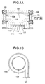
- Figs. 1A and 1B are views showing a microwave plasma processing apparatus as an example of the present invention.
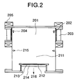
- Fig. 2 is a view showing a microwave isolation plasma processing apparatus as an example of the present invention.
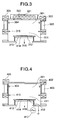
- Fig. 3 is a view showing a photo-assist microwave plasma processing apparatus as an example of the present invention.
- Fig. 4 is a view showing a bias microwave plasma processing apparatus as an example of the present invention.
- Figs. 5A and 5B are views showing a microwave plasma processing apparatus as an example of the prior art.
- Reference numeral 101 denotes a plasma generation chamber 101; 102, a quartz tube for constituting the plasma generation chamber 101; 103, a circular waveguide with slots for feeding a microwave into the plasma generation chamber 101; 104, a plasma generation gas supply means; 105, a magnetic field generation means for generating a cups magnetic field having a nodal surface on a plane including the center of the plurality of slots of the circular waveguide 103 and having a magnetic flux line almost perpendicular to the substrate support means, in which the magnetic flux density of a magnetic field near the slots is higher than the magnetic flux density of a magnetic field near the substrate; 111, a processing chamber communicating with the plasma generation chamber; 112, a substrate to be processed; 113, a support member for the substrate 112; 114, a heater for heating the substrate 112; 115, a process gas supply means; and 116, an exhaust.
- Reference numeral 120 denotes a plasma generation chamber 101; 102, a quartz tube for constituting the plasma generation chamber 101;
- Plasma generation and plasma processing are performed as follows.
- the plasma generation chamber 101 and the processing chamber 111 are evacuated through an exhaust system (not shown).
- a plasma generation gas is supplied into the plasma generation chamber 101 at a predetermined flow rate through the gas supply port 104.
- a conductance valve (not shown) arranged in the exhaust system (not shown) is adjusted to hold the plasma generation chamber 101 and the processing chamber 111 at a predetermined pressure.
- a cups magnetic field is generated in the plasma generation chamber 101 by the magnetic field generation means 105, and a desired power is supplied from a microwave power supply (not shown) into the plasma generation chamber 101 through the circular waveguide 103, thereby producing a plasma in the plasma generation chamber 101.
- the process gas when a process gas is supplied into the processing chamber 111 through the process gas supply means 115, the process gas is excited by the produced high-density plasma to form a film on the surface of the substrate to be processed 112 placed on the support member 113.
- the process gas may be supplied into the plasma generation gas supply port 104 depending on the application.
- the apparatus according to the present invention is characterized in that a cups magnetic field is generated in the plasma generation chamber.
- the cups magnetic field is generated between two coils having different polarities when the coils oppose each other.
- the magnetic flux lines are shown in Fig. 1A. Electrons are diffused along the magnetic flux lines on a long path extending from the portion near the slots to the portion near the substrate while rotating around the magnetic flux lines, and loss caused by diffusion and recombination of the electrons can be suppressed. For this reason, a high-density and large-area uniform plasma can be maintained even at a low temperature and even in a low-pressure region having a pressure of 1 mTorr or less.
- the magnetic field preferably has a nodal surface on a plane including the center of the plurality of slots of the circular waveguide with slots.
- the nodal surface on the plane including the center of the plurality of slots of the circular waveguide with slots is a surface on which the magnetic flux lines of the cups magnetic field are not traversed.
- cylindrical coils having the same polarity are vertically arranged through the circular waveguide. With this arrangement, magnetic flux lines which are almost perpendicular to the substrate support means and have a nodal surface on a plane including the center of the plurality of slots of the circular waveguide with slots are generated. Not only coils, but also permanent magnets can be used. When the coils are used, a cooling means such as a water-cooling means or an air-cooling means may be used to prevent over-heating.
- a frequency can be properly selected from the range of 0.8 GHz to 20 GHz.
- the waveguide used in the microwave plasma processing apparatus of the present invention may have a cylindrical shape, a disk-like shape, a polygon-like shape, or the like depending on the shape of the plasma generation chamber.
- Ultraviolet rays may be irradiated on the substrate surface to further improve the quality of processing.
- a light source any light source for emitting light rays which are absorbed by the substrate to be processed or gas adhered to the substrate can be applied.
- An excimer laser, an excimer lamp, a rare gas resonance line lamp, a low-pressure mercury lamp, or the like is properly used.
- a pressure in the generation chamber or processing chamber in the microwave plasma processing method of the present invention is selected from the range of 0.05 mTorr to 1.0 mTorr. According to CVD in a low-pressure region, the quality of a deposition film is improved.
- various deposition films such as an insulating film consisting of Si 3 N 4 , SiO 2 , Ta 2 O 5 , TiO 2 , TiN, Al 2 O 3 , AlN, MgF 2 , or the like, a semiconductor film consisting of a-Si, poly-Si, SiC, GaAs, or the like, and a metal film consisting of Al, W, Mo, Ti, Ta, or the like can be efficiently formed by properly selecting a gas to be used.
- a substrate used in the microwave plasma processing method of the present invention may be a semiconductor substrate, a conductive substrate, or an electrically insulating substrate. According to the apparatus of the present invention, deposition can be performed at a low temperature. For this reason, a substrate consisting a plastic or the like which has low heat resistance can be used.
- a metal such as Fe, Ni, Cr, Al, Mo, Nb, Ta, V, Ti, Pt, Pb, or the like or an alloy thereof, e.g., brass or stainless steel is available.
- a film sheet or the like consisting of SiO 2 -based quartz, various glasses, an inorganic matter such as Si 3 N 4 , NaCl, KCl, LiF, CaF 2, BaF 2 , Al 2 O 3 , AlN, or NgO, or an organic matter such as polyethylene, polyester, polycarbonate, cellulose acetate, polypropylene, polyvinylidene chloride, polystyrene, polyamide, or polyimide is available.
- a generally known gas can be used as a thin film forming gas.
- a gas which is easily resolved by the effect of a plasma and can be singularly deposited is desirably supplied into the film formation chamber through the film formation gas supply means or the like in the film formation chamber.
- a gas which is not easily resolved by the effect of the plasma and cannot be easily deposited is desirably supplied into the plasma generation chamber through the plasma generation gas supply port in the plasma generation chamber.
- a material containing Si atoms and supplied through the film formation gas supply means when an Si-based semiconductor thin film consisting of a-Si, poly-Si, SiC, or the like is formed As a material containing Si atoms and supplied through the film formation gas supply means when an Si-based semiconductor thin film consisting of a-Si, poly-Si, SiC, or the like is formed, a material which is in a gas state at an atmospheric temperature and an atmospheric pressure or a material which can be easily gasified is used.
- inorganic silanes such as SiH 4 and Si 2 H 6, organic silanes such as tetraethylsilane (TES), tetramethylsilane (TMS), and dimethylsilane (DMS), or halosilanes such as SiF 4 , Si 2 F 6 , SiHF 3 , SiH 2 F 2 , SiCl 4 , Si 2 Cl 6 , SiHCl 3 , SiH 2 Cl 2 , SiH 3 Cl, and SiC 2 F 2 are used.
- TES tetraethylsilane
- TMS tetramethylsilane
- DMS dimethylsilane
- halosilanes such as SiF 4 , Si 2 F 6 , SiHF 3 , SiH 2 F 2 , SiCl 4 , Si 2 Cl 6 , SiHCl 3 , SiH 2 Cl 2 , SiH 3 Cl, and SiC 2 F 2 are used.
- a plasma generation gas supplied through the plasma generation gas supply port in this case,
- a material containing Si atoms and supplied through the film formation gas supply means when an Si-compound-based thin film consisting of Si 3 N 4 , SiO 2 , or the like is formed As a material containing Si atoms and supplied through the film formation gas supply means when an Si-compound-based thin film consisting of Si 3 N 4 , SiO 2 , or the like is formed, a material which is in a gas state at an atmospheric temperature and an atmospheric pressure or a material which can be easily gasified is used.
- inorganic silanes such as SiH 4 and Si 2 H 6
- organic silanes such as tetraethoxysilane (TEOS), tetramethoxysilane (TMOS), and octamethyl cyclotetrasilane (OMCTS)
- halosilanes such as SiF 4 , Si 2 F 6 , SiHF 3 , SiH 2 F 2 , SiCl 4 , Si 2 Cl 6 , SiHCl 3 , SiH 2 Cl 2 , SiH 3 Cl, and SiCl 2 F 2 are used.
- N 2 , NH 3 , N 2 H 4 , hexamethyldisilane (HMDS), O 2 , O 3 , H 2 O, NO, N 2 O, or NO 2 can be used.
- an inorganic metal such as trimethylaluminum (TMAl), triethylaluminum (TEAl), triisobutylaluminum (TIBAl), dimethylaluminum hydride (DMAlH), tungsten carbonyl (W(CO) 6 ), molybdenum carbonyl (Mo(CO) 6 ), trimethylgallium (TMGa), or triethylgallium (TEGa), a metal halide such as AlCl 3 , WF 6 , TiCl 3 , or TaCl 5 can be used.
- a plasma generation gas supplied through the plasma generation gas supply port in this case, H 2 , He, Ne, Ar, Kr, Xe, or Rn can be used.
- an inorganic metal such as trimethylaluminum (TMAl), triethylaluminum (TEAl), triisobutylaluminum (TIBAl), dimethylaluminum hydride (DMAlH), tungsten carbonyl (W(CO) 6 ), molybdenum carbonyl (Mo(CO) 6 ), trimethylgallium (TMGa), or triethylgallium (TEGa) can be used.
- TMAl trimethylaluminum
- TEAl triethylaluminum
- TIBAl triisobutylaluminum
- DMAlH dimethylaluminum hydride
- W(CO) 6 molybdenum carbonyl
- Mo(CO) 6 trimethylgallium
- TMGa triethylgallium
- a metal halide such as AlCl 3 , WF 6 , TiCl 3 , or TaCl 5 can be used.
- As a plasma generation gas supplied through the plasma generation gas supply port in this case O 2 , O 3 , H 2 O, NO, N 2 O, NO 2 , N 2 , NH 3 , N 2 H 4 , hexamethyldisilane (HMDS), or the like can be used.
- HMDS hexamethyldisilane
- the microwave plasma processing apparatus of the present invention can also be applied to surface modification.
- a gas to be used is properly selected, Si, Al, Ti, Zn, Ta, or the like is used as a substrate or a surface layer, and an oxidizing process, a nitriding process, and a doping process of B, As, P, or the like can be performed.
- a film formation technique employed in the present invention can also be applied to a cleaning method. In this case, the film formation technique can be applied to cleaning for an oxide, an inorganic matter, or a heavy metal. The film formation technique can also be properly used for ashing.
- oxidizing gas supplied through the plasma generation gas supply port when the substrate is subjected to an oxidizing surface process O 2 , O 3 , H 2 O, NO, N 2 O, NO 2 , or the like can be used.
- a nitriding gas supplied through the plasma generation gas supply means when the substrate is subjected to a nitriding surface process N 2 , NH 3 , N 2 H 4 , hexamethyldisilane (HMDS), or the like can be used.
- HMDS hexamethyldisilane
- a cleaning gas supplied from the plasma generation gas supply port when the inorganic matter is cleaned from the substrate surface O 2 , O 3 , H 2 O, NO, N 2 O, NO 2 , or the like can be used.
- a cleaning gas supplied from the plasma generation gas supply port when the organic matter is cleaned from the substrate surface F 2 , CF 4 , CH 2 F 2 , C 2 F 6 , CF 2 Cl 2 , SF 6 , NF 3 , or the like can be used. In this case, since film formation is not performed, a source gas is not supplied through the film formation gas supply means, or the same gas as the gas supplied through the plasma generation gas supply port is supplied.
- a microwave plasma processing apparatus and a processing method according to the present invention will be described below in detail with reference to the following apparatus examples. However, the present invention is not limited to these examples.
- the apparatus shown in Figs. 1A and 1B was manufactured in the following manner.
- the circular waveguide 103 has an internal wall section having a size of 27 mm ⁇ 96 mm equal to that of a waveguide according to WRT-2 standards, and has a central diameter of 354 mm.
- the material of the circular waveguide 103 is stainless steel to keep the mechanical strength of the circular waveguide 103.
- Two-layered plating is performed to the inner wall surface of the circular waveguide 103 in such a manner that silver is coated on a copper plate to suppress propagation loss of a microwave.
- slots for feeding a microwave into the plasma generation chamber 101 are formed.
- Each slot has a rectangular shape having a size of 42 mm (length) ⁇ 2 mm (width), and the slots are formed at intervals each of which is 1/4 a guide wave length.
- the guide wave length depends on the frequency of a microwave and the size of the section of the waveguide. When a microwave having a frequency of 2.45 GHz and a waveguide having the above size are used, the guide wave length is about 159 mm. In the circular waveguide 103 used in this case, 28 slots are formed at about 40 mm intervals.
- a 4E tuner, a directional coupler, an isolator, and a microwave power supply (not shown) having a frequency of 2.45 GHz are sequentially connected to the circular waveguide 103.
- Plasma generation and plasma processing are performed as follows.
- the plasma generation chamber 101 and the processing chamber 111 are evacuated through an exhaust system (not shown).
- a plasma generation gas is supplied into the plasma generation chamber 101 at a predetermined flow rate through the gas supply port 104.
- a conductance valve (not shown) arranged in the exhaust system (not shown) is adjusted to hold the plasma generation chamber 101 and the processing chamber 111 at a predetermined pressure.
- a desired magnetic field is generated in the plasma generation chamber 101 through the magnetic field generation means 105, and a desired power is supplied from a microwave power supply (not shown) through the circular waveguide 103, thereby producing a plasma in the plasma generation chamber 101.
- the process gas when a process gas is supplied into the processing chamber 111 through the process gas supply means 115, the process gas is excited by the produced high-density plasma to process the surface of the substrate to be processed 112 placed on the support member 113.
- the process gas may be supplied into the plasma generation gas supply port 104 depending on the application.
- a plasma was produced under the conditions: an Ar flow rate of 500 sccm; a pressure of 1 mTorr; a microwave power of 3.0 kW, and a maximum magnetic flux density of 90 mT.
- the produced plasma was measured by a single probe method in the following manner. A voltage applied to the probe was changed within the range of -50 to +50 V, and a current flowing in the probe was measured by an I-V meter. An electron density, an electron temperature, and a plasma potential were calculated on the basis of the obtained I-V curve by Langmiuir's method. As a result, the electron density was 2.7 ⁇ 10 12 /cm 3 (in ⁇ 200 plane), and the electron temperature was 3.6 eV. It was confirmed that a high-density plasma was formed although the pressure was set to be low.
- FIG. 2 An isolation plasma processing apparatus which is an example of the present invention is shown in Fig. 2.
- Reference numeral 201 denotes a plasma generation chamber 201; 202, a quartz tube for constituting the plasma generation chamber 201; 203, a circular waveguide with slots for feeding a microwave into the plasma generation chamber 201; 204, a plasma generation gas supply means; 205, a magnetic field generation means; 211, a processing chamber communicating with the plasma generation chamber; 212, a substrate to be processed; 213, a support member for the substrate 212; 214, a heater for heating the substrate 212; 215, a process gas supply means; and 216, an exhaust.
- Apparatus Example 2 is different from Apparatus Example 1 in that a plasma-substrate interval in Apparatus Example 2 is larger than that in Apparatus Example 1 by 100 mm.
- Plasma generation and plasma processing are performed as follows.
- the plasma generation chamber 201 and the processing chamber 211 are evacuated through an exhaust system (not shown).
- a plasma generation gas is supplied into the plasma generation chamber 201 at a predetermined flow rate through the gas supply port 204.
- a conductance valve (not shown) arranged in the exhaust system (not shown) is adjusted to hold the plasma generation chamber 201 at a predetermined pressure.
- a desired power is supplied from a DC power supply (not shown) to the coil 205 to generate a magnetic field in the plasma generation chamber 201, and a desired power is supplied from a microwave power supply (not shown) into the plasma generation chamber 201 through the circular waveguide 203.
- Electrons spirally moving around magnetic flux lines generated in the plasma generation chamber 201 by the magnetic field generation means 205 resonantly absorb the microwave to be accelerated, thereby generating a higher-density plasma in the plasma generation chamber 201.
- the process gas reacts with the plasma generation gas excited by the produced high-density plasma to process the surface of the substrate to be processed 212 placed on the support member 213.
- the process gas may be supplied into the plasma generation gas supply port 204 depending on the application.
- FIG. 3 A photo-assistant processing apparatus which is an example of the present invention is shown in Fig. 3.
- Reference numeral 301 denotes a plasma generation chamber 301; 302, a quartz tube for constituting the plasma generation chamber 301; 303, a circular waveguide with slots for feeding a microwave into the plasma generation chamber 301; 304, a plasma generation gas supply means; 305, a magnetic field generation means; 311, a processing chamber communicating with the plasma generation chamber; 312, a substrate to be processed; 313, a support member for the substrate 312; 314, a heater for heating the substrate 312; 315, a process gas supply means; 316, an exhaust; 321, a lighting system for irradiating ultraviolet rays onto the surface of the substrate 312; and 322, a light guide window for guiding visible ultraviolet rays from the lighting system 321 to the processing chamber 311 through the plasma generation chamber 301.
- Plasma generation and plasma processing are performed as follows.
- the plasma generation chamber 301 and the processing chamber 311 are evacuated through an exhaust system (not shown). Visible ultraviolet rays from the lighting system 321 are irradiated onto the surface of the substrate 312 through the light guide window 322, and the substrate 312 is held at a desired temperature.
- a plasma generation gas is supplied into the plasma generation chamber 301 at a predetermined flow rate through the gas supply port 304.
- a conductance valve (not shown) arranged in the exhaust system (not shown) is adjusted to hold the plasma generation chamber 301 at a predetermined pressure.
- a magnetic field is generated in the plasma generation chamber 301 through the magnetic field generation means 305, and a desired power is supplied from a microwave power supply (not shown) through the circular waveguide 303, thereby producing a plasma in the plasma generation chamber 301.
- a process gas is supplied into the processing chamber 311 through the process gas supply means 315, the process gas is excited by the produced high-density plasma to process the surface of the substrate to be processed 312 placed on the support member 313.
- the process gas may be supplied into the plasma generation gas supply port 304 depending on the application.
- any light source having a wavelength absorbed by the substrate surface or the gas or a precursor adhered to the substrate surface can be used. That is, a low-pressure mercury lamp, a xenon-mercury lamp, a heavy hydrogen lamp, an Ar resonance line lamp, a Kr resonance line lamp, a Xe resonance line lamp, an excimer lamp, an excimer laser, an Ar + laser harmonic wave, an N 2 laser, or a YAG laser harmonic wave can be used.
- Reference numeral 401 denotes a plasma generation chamber 401; 402, a quartz tube for constituting the plasma generation chamber 401; 403, a circular waveguide with slots for feeding a microwave into the plasma generation chamber 401; 404, a plasma generation gas supply means; 405, a magnetic field generation means; 411, a plasma generation chamber communicating with the plasma generation chamber; 412, a substrate to be processed; 413, a support member for the substrate 412; 414, a heater for heating the substrate 412; 415, a process gas supply means; 416, an exhaust; and 417, a high-frequency supply means for applying a bias to the substrate support member 412.
- Plasma generation and plasma processing are performed as follows.
- the plasma generation chamber 401 and the processing chamber 411 are evacuated through an exhaust system (not shown).
- the substrate 412 is heated to a desired temperature through the heater 414, and held at the desired temperature.
- a plasma generation gas is supplied into the plasma generation chamber 401 at a predetermined flow rate through the gas supply port 404.
- a conductance valve (not shown) arranged in the exhaust system (not shown) is adjusted to hold the plasma generation chamber 401 at a predetermined pressure.
- a magnetic field is generated in the plasma generation chamber 401 through the magnetic field generation means 405, and a desired power is supplied from a microwave power supply (not shown) through the circular waveguide 403, thereby producing a plasma in the plasma generation chamber 401.
- a high-frequency wave is applied to the substrate support member 413 through the high-frequency supply means 417 to generate a self-bias on the substrate surface.
- the process gas is excited by the produced high-density plasma to accelerate generated ions by the self-bias, thereby processing the surface of the substrate to be processed 412 placed on the support member 413.
- the process gas may be supplied into the plasma generation gas supply port 404 depending on the application.
- the frequency of the high-frequency supply means 417 is optimally set to be 100 kHz to 20 MHz, more optimally, 1 MHz to 5 MHz in consideration of discharge stability and the self-bias.
- a microwave plasma CVD method according to the present invention will be described in detail with reference to processing method examples of the present invention.
- the present invention is not limited to these examples.
- a silicon nitride film for an optomagnetic disk was formed by using the microwave plasma processing apparatus shown in Figs. 1A and 1B.
- a polycarbonate (PC) substrate ( ⁇ 3.5 inches) with a 1.2 ⁇ m width group was used.
- the PC substrate 112 was placed on the substrate support member 113, and the plasma generation chamber 101 and the film formation chamber 111 were evacuated through an exhaust system (not shown) to reduce the pressure in the plasma generation chamber 101 and the film formation chamber 111 to 10 -6 Torr.
- a nitrogen gas was supplied at a flow rate of 100 sccm through the plasma generation gas supply port 104, and an argon gas was supplied into the plasma generation chamber 101 at a flow rate of 600 sccm.
- a monosilane gas was supplied into the film formation chamber 111 at a flow rate of 200 sccm through the film formation gas supply means 115.
- a conductance valve (not shown) arranged in the exhaust system (not shown) was adjusted to hold the pressure in the film formation chamber 111 at 5 mTorr.
- a magnetic field having a maximum magnetic flux density of 90 mT was generated in the plasma generation chamber 101 through the magnetic field generation means 105, and a 3.0-kW power was supplied from a 2.45-GHz microwave power supply through the circular waveguide 103. In this manner, a plasma was produced in the plasma generation chamber 101.
- the nitrogen gas supplied through the plasma generation gas supply means 104 was excited and resolved in the plasma generation chamber 101 to be active seeds, and the active seeds were transported toward the silicon substrate 112 to react with the monosilane gas supplied through the film formation gas supply means 115, thereby forming a silicon nitride film having a thickness of 100 nm on the silicon substrate 112 within 12 seconds.
- film quality such as a refractive index was evaluated.
- the film formation rate of the obtained silicon nitride film was very high, i.e., 500 nm/min, and that a high-quality film having a refractive index of 2.2, good adhesion, and good durability could be obtained.
- the density of the film was 2.9 g/cm 3 . Therefore, the film having a density higher than that (2.7 g/cm 3 ) of a film formed without supplying a magnetic field was formed.
- a silicon oxide film for preventing plastic lens reflection and a silicon nitride film were formed by using the microwave plasma processing apparatus shown in Figs. 1A and 1B.
- a plastic convex lens having a diameter of 50 mm was used as the substrate 112 as the substrate 112.
- the PC substrate 112 was placed on the substrate support member 113, and the plasma generation chamber 101 and the film formation 111 were evacuated through an exhaust system (not shown) to reduce the pressure in the plasma generation chamber 101 and the film formation 111 to 10 -6 Torr.
- a nitrogen gas was supplied at a flow rate of 150 sccm through the plasma generation gas supply means 104.
- a monosilane gas was supplied into the film formation chamber 111 at a flow rate of 100 sccm through the film formation gas supply means 115.
- a conductance valve (not shown) arranged in the exhaust system (not shown) was adjusted to hold the pressure in the film formation chamber 111 at 1 mTorr.
- a power was supplied from a DC power supply (not shown) to a coil 106 to generate a magnetic field having a maximum magnetic flux density of 90 mT in the plasma generation chamber 101, and a 3.0-kW power was supplied from a 2.45-GHz microwave power supply (not shown) into the plasma generation chamber 101 through the circular waveguide 103. In this manner, a plasma was produced in the plasma generation chamber 101.
- the nitrogen gas supplied through the plasma generation gas supply means 104 was excited and resolved in the plasma generation chamber 101 to be active seeds such as nitrogen atoms, and the active seeds were transported toward the lens 112 to react with the monosilane gas supplied through the film formation gas supply means 115, thereby forming a silicon nitride film having a thickness of 21 nm on the lens 112.
- An oxygen gas was supplied at a flow rate of 200 sccm into the plasma generation chamber 101 through the plasma generation gas supply means 104.
- a monosilane gas was supplied into the film formation chamber 111 at a flow rate of 100 sccm through the film formation gas supply means 115.
- a conductance valve (not shown) arranged in the exhaust system (not shown) was adjusted to hold the pressure in the film formation chamber 111 at 1 mTorr.
- a power was supplied from a DC power supply (not shown) to a coil 106 to generate a magnetic field having a maximum magnetic flux density of 90 mT in the plasma generation chamber 101, and a 2.0-kW power was supplied from a 2.45-GHz microwave power supply (not shown) into the plasma generation chamber 101 through the circular waveguide 103. In this manner, a plasma was produced in the plasma generation chamber 101.
- the oxygen gas supplied through the plasma generation gas supply means 104 was excited and resolved in the plasma generation chamber 101 to be active seeds such as oxygen atoms, and the active seeds were transported toward the glass substrate 112 to react with the monosilane gas supplied through the film formation gas supply means 115, thereby forming a silicon oxide film having a thickness of 86 nm on the glass substrate 112.
- a film formation rate and reflection characteristics were evaluated.
- the formation rates of the silicon nitride film and the silicon oxide film were very high, i.e., 300 nm/min and 360 nm/min, respectively, and that extremely preferable optical characteristics could be obtained, e.g., a reflectance at about 500 nm was 0.3%.
- a silicon nitride film for protecting a semiconductor element was formed by using the microwave plasma processing apparatus shown in Figs. 1A and 1B.
- a p-type monocrystalline silicon substrate (plane orientation ⁇ 100 ⁇ , resistivity: 10 ⁇ cm) with an interlayer SiO 2 film on which an Al wiring pattern (line and space: 0.5 ⁇ m) was formed was used.
- the plasma generation chamber 101 and the film formation chamber 111 were evacuated through an exhaust system (not shown) to reduce the pressure in the plasma generation chamber 101 and the film formation 111 to 10 -6 Torr.
- a heater (not shown) was turned on to heat the substrate 112 to 300°C, and the substrate was held at this temperature.
- a nitrogen gas was supplied at a flow rate 500 sccm into the plasma generation chamber 101 through the plasma generation gas supply port 104.
- a monosilane gas was supplied into the film formation chamber 111 at a flow rate of 100 sccm through the film formation gas supply means 115.
- a conductance valve (not shown) arranged in the exhaust system (not shown) was adjusted to hold the pressure in the film formation chamber 111 at 5 mTorr.
- a power was supplied from a DC power supply (not shown) to a coil 106 to generate a magnetic field having a maximum magnetic flux density of 90 mT in the plasma generation chamber 101, and a 3.0-kW power was supplied from a 2.45-GHz microwave power supply (not shown) through the circular waveguide 103. In this manner, a plasma was produced in the plasma generation chamber 101.
- the nitrogen gas supplied through a plasma generation gas supply means 108 was excited and resolved in the plasma generation chamber 101 to be active seeds, and the active seeds were transported toward the silicon substrate 112 to react with the monosilane gas supplied through the film formation gas supply means 115, thereby forming a silicon nitride film having a thickness of 1.0 ⁇ m on the silicon substrate 112.
- a film formation rate and film quality such as stress were evaluated. The stress was calculated such that an amount of warpage of the substrate after and before film formation was measured by a laser interferometer Zygo (trade name).
- the formation rate of the silicon nitride film was very high, i.e., 460 nm/min, and that an extremely high-quality film having a stress of 1.1 ⁇ 10 9 dyn/cm 2 (compression), a leakage current of 1.2 ⁇ 10 -10 A/cm 2 , and a breakdown voltage of 9 MV/cm could be obtained.
- a BPSG film for a semiconductor element was etched by using the microwave plasma processing apparatus shown in Figs. 1A and 1B.
- a p-type monocrystalline silicon substrate (plane orientation ⁇ 100 ⁇ , resistivity: 10 ⁇ cm) on which a BPSG film having a thickness of 1 ⁇ m was formed on a polysilicon pattern (line and space: 0.5 ⁇ m) was used.
- the plasma generation chamber 101 and the film formation chamber 111 were evacuated through an exhaust system (not shown) to reduce the pressure in the plasma generation chamber 101 and the film formation 111 to 10 -6 Torr.
- a CF 4 gas was supplied at a flow rate of 300 sccm into the plasma generation chamber 101 through the plasma generation gas supply means 104.
- a conductance valve (not shown) arranged in the exhaust system (not shown) was adjusted to hold the pressure in the film formation chamber 111 at 0.5 mTorr.
- a power was supplied from a DC power supply (not shown) to a coil 106 to generate a magnetic field having a maximum magnetic flux density of 90 mT in the plasma generation chamber 101, and a 1.5-kW power was supplied from a 2.45-GHz microwave power supply through the circular waveguide 103.
- a plasma was produced in the plasma generation chamber 101.
- the CF 4 gas supplied through a plasma generation gas supply means 104 was excited and resolved in the plasma generation chamber 101 to be active seeds, and the active seeds were transported toward the silicon substrate 112 to etch the BPSG film.
- a selectivity ratio of etching rates and an etching shape were evaluated. The etching shape was evaluated such that the section of an etched silicon oxide film was observed with a scanning electron microscope (SEM).
- the etching rate and the selectivity ratio of the etching rate of the BPSG film to the etching rate of a polysilicon film were preferable, i.e., 300 nm/min and 30, respectively, that the etching shape was almost perpendicular, and that a microloading effect was small.
- a silicon oxide film for insulating a semiconductor element gate was formed by using the isolation plasma processing apparatus shown in Fig. 2.
- a p-type monocrystalline silicon substrate (plane orientation ⁇ 100 ⁇ , resistivity: 10 ⁇ cm) was used.
- the plasma generation chamber 201 and the film formation chamber 211 were evacuated through an exhaust system (not shown) to reduce the pressure in the plasma generation chamber 201 and the film formation 211 to 10 -6 Torr.
- a heater (not shown) was turned on to heat the silicon substrate 212 to 300°C, and the substrate 212 was held at this temperature.
- An oxygen gas was supplied at a flow rate of 200 sccm into the plasma generation chamber 201 through the plasma generation gas supply means 204.
- a monosilane gas was supplied into the film formation chamber 211 at a flow rate of 50 sccm through the film formation gas supply means 215.
- a conductance valve (not shown) arranged in the exhaust system (not shown) was adjusted to hold the pressure in the film formation chamber 211 at 20 mTorr.
- a power was supplied from a DC power supply (not shown) to a coil 206 to generate a magnetic field having a maximum magnetic flux density of 90 mT in the plasma generation chamber 201, and a 1.5-kW power was supplied from a 2.45-GHz microwave power supply into the plasma generation chamber 201 through the circular waveguide 203. In this manner, a plasma was produced in the plasma generation chamber 201.
- the oxygen gas supplied through the plasma generation gas supply means 204 was excited and resolved in the plasma generation chamber 201 to be active seeds such as oxygen atoms, and the active seeds were transported toward the silicon substrate 212 to react with the monosilane gas supplied through the film formation gas supply means 215, thereby forming a silicon oxide film having a thickness of 0.1 ⁇ m on the silicon substrate 212.
- a film formation rate, uniformity, a leakage current, a breakdown voltage, and an interfacial level density were evaluated.
- the interfacial level density was calculated on the basis of a C-V curve obtained when a high-frequency wave of 1 MHz obtained by a capacity measuring device was applied.
- the film formation rate and uniformity of the silicon oxide film were preferable, i.e., 110 nm/min ⁇ 2.3% and that an extremely high-quality film having a leakage current of 4 ⁇ 10 -11 A/cm 2 , a breakdown voltage of 11 MV/cm, and an interfacial level density of 6 ⁇ 10 10 cm -2 could be obtained.
- a silicon oxide film for insulating semiconductor element layers from each other was formed by using a photo-assistant microwave plasma processing apparatus shown in Fig. 3.
- a p-type monocrystalline silicon substrate (plane orientation ⁇ 100 ⁇ , resistivity: 10 ⁇ cm) on which an Al pattern (line and space: 0.5 ⁇ m) was formed on the uppermost portion was used.
- the silicon substrate 312 was placed on the substrate support member 313, the plasma generation chamber 301 and the film formation chamber 311 were evacuated through an exhaust system (not shown) to reduce the pressure in the plasma generation chamber 301 and the film formation 311 to 10 -6 Torr.
- a KrCl* excimer lamp of the lighting system 321 was turned on to irradiate light onto the surface of the silicon substrate 312 such that an illuminance on the surface was set to be 20 mW/cm 2 .
- a heater (not shown) was turned on to heat the silicon substrate 312 to 300°C, and the substrate 312 was held at this temperature.
- An oxygen gas was supplied at a flow rate of 500 sccm into the plasma generation chamber 311 through the plasma generation gas supply means 304.
- a tetraethoxysilane (TEOS) gas was supplied into the film formation chamber 311 at a flow rate of 200 sccm from the film formation gas supply means 315 into the film formation chamber 311.
- a conductance valve (not shown) arranged in the exhaust system (not shown) was adjusted to hold the pressure in the plasma generation chamber 301 at 0.1 mTorr and to hold the pressure in the film formation chamber 311 at 0.5 Torr.
- a power was supplied from a DC power supply (not shown) to a coil 306 to generate a magnetic field having a maximum magnetic flux density of 90 mT in the plasma generation chamber 301, and a 1.5-kW power was supplied from a 2.45-GHz microwave power supply into the plasma generation chamber 301 through the circular waveguide 303. In this manner, a plasma was produced in the plasma generation chamber 301.
- the oxygen gas supplied through the plasma generation gas supply means 304 was excited and resolved in the plasma generation chamber 301 to be active seeds, and the active seeds were transported toward the silicon substrate 312 to react with the tetraethoxysilane gas supplied through the film formation gas supply means 315, thereby forming a silicon oxide film having a thickness of 0.8 ⁇ m on the silicon substrate 312.
- a film formation rate, uniformity, a breakdown voltage, and step coverage were evaluated.
- the step coverage was evaluated such that the section of the silicon oxide film formed on the Al wiring pattern was observed by a scanning electron microscope (SEM) to calculate a ratio (cover factor) of a film thickness on a side wall of the step to a film thickness on the step.
- SEM scanning electron microscope
- the film formation rate and uniformity of the silicon oxide film were preferable, i.e., 180 nm/min ⁇ 2.7% and that an extremely high-quality film having a breakdown voltage of 9.3 MV/cm and a cover factor of 0.9 could be obtained.
- a polysilicon film between semiconductor element gate electrodes was etched by using the bias plasma processing apparatus shown in Fig. 4.
- the substrate 412 As the substrate 412, a p-type monocrystalline silicon substrate (plane orientation ⁇ 100 ⁇ , resistivity: 10 ⁇ cm) on which a polysilicon film was formed on the uppermost portion was used. After the silicon substrate 412 was placed on the substrate support member 413, the plasma generation chamber 401 and the etching chamber 411 were evacuated through an exhaust system (not shown) to reduce the pressure in the plasma generation chamber 401 and the etching chamber 411 to 10 -6 Torr. A CF 4 gas and an oxygen gas were supplied at flow rates of 300 sccm and 20 sccm into the plasma generation chamber 411 through the plasma generation gas supply means 404, respectively.
- a conductance valve (not shown) arranged in the exhaust system (not shown) was adjusted to hold the pressure in the plasma generation chamber 401 at 0.5 mTorr.
- a power was supplied from a DC power supply (not shown) to a coil 406 to generate a magnetic field having a maximum magnetic flux density of 90 mT in the plasma generation chamber 401, and a 5-kW power was supplied from a 2.45-GHz microwave power supply into the plasma generation chamber 401 through the circular waveguide 403. In this manner, a plasma was produced in the plasma generation chamber 401.
- the CF 4 gas and oxygen gas supplied through a plasma generation gas supply means 404 were excited and resolved in the plasma generation chamber 401 to be active seeds, and the active seeds were transported toward the silicon substrate 412 to etch the polysilicon film by ions accelerated by a self-bias. After etching, an etching rate, a selectivity ratio, and an etching shape were evaluated. The etching shape was evaluated such that the section of the etched polysilicon film was observed with a scanning electron microscope (SEM).
- SEM scanning electron microscope
- the etching rate and the selectivity ratio of the etching rate of the polysilicon film to the etching rate of an SiO 2 film were preferable, i.e., 600 nm/min and 30, respectively, that the perpendicularity of the etching shape was higher than that of an etching shape obtained without applying a high-frequency wave, and that a microloading effect was small.
- a microwave plasma processing apparatus comprises a plasma generation chamber, a processing chamber communicating with the plasma generation chamber, supporting of a substrate to be processed arranged in the processing chamber, a circular waveguide with slots arranged around the plasma generation chamber, and magnetic field generation unit for generating a cusp magnetic field in the plasma generation chamber.
- a microwave plasma processing method using this apparatus are provided, to maintain a high-density and large-area uniform plasma, even at a low temperature, and even in a low-pressure region having a pressure of 1 mTorr.
Landscapes
- Chemical & Material Sciences (AREA)
- Engineering & Computer Science (AREA)
- Physics & Mathematics (AREA)
- Plasma & Fusion (AREA)
- Analytical Chemistry (AREA)
- Chemical Kinetics & Catalysis (AREA)
- General Chemical & Material Sciences (AREA)
- Materials Engineering (AREA)
- Mechanical Engineering (AREA)
- Metallurgy (AREA)
- Organic Chemistry (AREA)
- Drying Of Semiconductors (AREA)
- Chemical Vapour Deposition (AREA)
- Plasma Technology (AREA)
Applications Claiming Priority (3)
| Application Number | Priority Date | Filing Date | Title |
|---|---|---|---|
| JP243375/95 | 1995-09-21 | ||
| JP24337595 | 1995-09-21 | ||
| JP7243375A JPH0987851A (ja) | 1995-09-21 | 1995-09-21 | マイクロ波プラズマ処理装置及び処理方法 |
Publications (3)
| Publication Number | Publication Date |
|---|---|
| EP0764969A2 true EP0764969A2 (fr) | 1997-03-26 |
| EP0764969A3 EP0764969A3 (fr) | 1997-11-12 |
| EP0764969B1 EP0764969B1 (fr) | 2002-12-04 |
Family
ID=17102922
Family Applications (1)
| Application Number | Title | Priority Date | Filing Date |
|---|---|---|---|
| EP96115091A Expired - Lifetime EP0764969B1 (fr) | 1995-09-21 | 1996-09-19 | Appareil de traitement par plasma micro-ondes et méthode de traitement par plasma micro-ondes |
Country Status (5)
| Country | Link |
|---|---|
| US (1) | US5985091A (fr) |
| EP (1) | EP0764969B1 (fr) |
| JP (1) | JPH0987851A (fr) |
| KR (1) | KR100220132B1 (fr) |
| DE (1) | DE69625149D1 (fr) |
Cited By (2)
| Publication number | Priority date | Publication date | Assignee | Title |
|---|---|---|---|---|
| US6531193B2 (en) | 1997-07-07 | 2003-03-11 | The Penn State Research Foundation | Low temperature, high quality silicon dioxide thin films deposited using tetramethylsilane (TMS) for stress control and coverage applications |
| EP3291279A1 (fr) * | 2016-09-06 | 2018-03-07 | Nano Coatings, S.L. | Systeme et procede de production de diamant par depot chimique en phase vapeur par plasma alimente d'energie micro-onde et assiste par laser |
Families Citing this family (23)
| Publication number | Priority date | Publication date | Assignee | Title |
|---|---|---|---|---|
| US6274459B1 (en) | 1998-02-17 | 2001-08-14 | Silicon Genesis Corporation | Method for non mass selected ion implant profile control |
| JP3352418B2 (ja) | 1999-01-28 | 2002-12-03 | キヤノン株式会社 | 減圧処理方法及び減圧処理装置 |
| JP2000312045A (ja) * | 1999-02-26 | 2000-11-07 | Tadahiro Omi | レーザ発振装置、露光装置及びデバイスの製造方法 |
| US6458723B1 (en) | 1999-06-24 | 2002-10-01 | Silicon Genesis Corporation | High temperature implant apparatus |
| JP3419745B2 (ja) * | 2000-02-28 | 2003-06-23 | キヤノン販売株式会社 | 半導体装置及びその製造方法 |
| JP2001267291A (ja) * | 2000-03-16 | 2001-09-28 | Nec Corp | 回路処理方法および装置、動作制御方法および装置、情報記憶媒体 |
| US6873113B2 (en) | 2000-04-13 | 2005-03-29 | Tokyo Electron Limited | Stand alone plasma vacuum pump |
| US6541781B1 (en) * | 2000-07-25 | 2003-04-01 | Axcelis Technologies, Inc. | Waveguide for microwave excitation of plasma in an ion beam guide |
| JP4610126B2 (ja) | 2001-06-14 | 2011-01-12 | 株式会社神戸製鋼所 | プラズマcvd装置 |
| US6729850B2 (en) | 2001-10-31 | 2004-05-04 | Tokyo Electron Limited | Applied plasma duct system |
| US7219403B2 (en) * | 2002-07-23 | 2007-05-22 | The Procter & Gamble Company | Fastening member comprising shaped tab |
| WO2007067086A1 (fr) * | 2005-12-08 | 2007-06-14 | Georgiy Yakovlevitch Pavlov | Dispositif de traitement par plasma |
| RU2368032C1 (ru) * | 2005-12-08 | 2009-09-20 | Георгий Яковлевич Павлов | Устройство плазменной обработки |
| KR100927995B1 (ko) * | 2008-11-20 | 2009-11-24 | 한국기초과학지원연구원 | 전자 맴돌이 공명 이온원 장치 및 그의 제조방법 |
| US8298372B2 (en) * | 2009-04-20 | 2012-10-30 | Applied Materials, Inc. | Quartz window having gas feed and processing equipment incorporating same |
| TWI465158B (zh) * | 2011-01-12 | 2014-12-11 | Ind Tech Res Inst | 微波電漿激發裝置 |
| US20140042152A1 (en) * | 2012-08-08 | 2014-02-13 | Taiwan Semiconductor Manufacturing Company, Ltd. | Variable frequency microwave device and method for rectifying wafer warpage |
| US9435031B2 (en) | 2014-01-07 | 2016-09-06 | International Business Machines Corporation | Microwave plasma and ultraviolet assisted deposition apparatus and method for material deposition using the same |
| JP6527482B2 (ja) | 2016-03-14 | 2019-06-05 | 東芝デバイス&ストレージ株式会社 | 半導体製造装置 |
| WO2020069901A1 (fr) * | 2018-10-02 | 2020-04-09 | Evatec Ag | Appareil de dépôt de couche atomique assisté par plasma (peald) |
| JP2023550342A (ja) * | 2020-11-20 | 2023-12-01 | ラム リサーチ コーポレーション | 静磁場を使用するプラズマ一様性制御 |
| KR102780461B1 (ko) * | 2022-09-07 | 2025-03-11 | 한국핵융합에너지연구원 | 공진 도파관에 의한 플라즈마 발생장치 |
| KR102888907B1 (ko) * | 2022-09-07 | 2025-11-19 | 한국핵융합에너지연구원 | 튜너를 구비하는 공진 도파관에 의한 플라즈마 발생장치 |
Family Cites Families (9)
| Publication number | Priority date | Publication date | Assignee | Title |
|---|---|---|---|---|
| DE3750115T2 (de) * | 1986-10-20 | 1995-01-19 | Hitachi Ltd | Plasmabearbeitungsgerät. |
| US5370765A (en) * | 1989-03-09 | 1994-12-06 | Applied Microwave Plasma Concepts, Inc. | Electron cyclotron resonance plasma source and method of operation |
| US5133826A (en) * | 1989-03-09 | 1992-07-28 | Applied Microwave Plasma Concepts, Inc. | Electron cyclotron resonance plasma source |
| EP0418540A3 (en) * | 1989-08-11 | 1991-08-07 | Sanyo Electric Co., Ltd. | Dry etching method |
| JP3042127B2 (ja) * | 1991-09-02 | 2000-05-15 | 富士電機株式会社 | 酸化シリコン膜の製造方法および製造装置 |
| JP2886752B2 (ja) * | 1991-11-05 | 1999-04-26 | キヤノン株式会社 | 無端環状導波管を有するマイクロ波導入装置及び該装置を備えたプラズマ処理装置 |
| US5487875A (en) * | 1991-11-05 | 1996-01-30 | Canon Kabushiki Kaisha | Microwave introducing device provided with an endless circular waveguide and plasma treating apparatus provided with said device |
| DE4235914A1 (de) * | 1992-10-23 | 1994-04-28 | Juergen Prof Dr Engemann | Vorrichtung zur Erzeugung von Mikrowellenplasmen |
| DE69419968T2 (de) * | 1993-05-27 | 2000-04-06 | Canon K.K. | Bearbeitungsgerät mittels Mikrowellen und Verfahren zur Herstellung eines anorganischen dielektrischen Films |
-
1995
- 1995-09-21 JP JP7243375A patent/JPH0987851A/ja active Pending
-
1996
- 1996-09-16 US US08/714,445 patent/US5985091A/en not_active Expired - Lifetime
- 1996-09-19 DE DE69625149T patent/DE69625149D1/de not_active Expired - Lifetime
- 1996-09-19 EP EP96115091A patent/EP0764969B1/fr not_active Expired - Lifetime
- 1996-09-20 KR KR19960041213A patent/KR100220132B1/ko not_active Expired - Fee Related
Cited By (2)
| Publication number | Priority date | Publication date | Assignee | Title |
|---|---|---|---|---|
| US6531193B2 (en) | 1997-07-07 | 2003-03-11 | The Penn State Research Foundation | Low temperature, high quality silicon dioxide thin films deposited using tetramethylsilane (TMS) for stress control and coverage applications |
| EP3291279A1 (fr) * | 2016-09-06 | 2018-03-07 | Nano Coatings, S.L. | Systeme et procede de production de diamant par depot chimique en phase vapeur par plasma alimente d'energie micro-onde et assiste par laser |
Also Published As
| Publication number | Publication date |
|---|---|
| JPH0987851A (ja) | 1997-03-31 |
| EP0764969A3 (fr) | 1997-11-12 |
| KR100220132B1 (ko) | 1999-09-01 |
| KR970015781A (fr) | 1997-04-28 |
| EP0764969B1 (fr) | 2002-12-04 |
| DE69625149D1 (de) | 2003-01-16 |
| US5985091A (en) | 1999-11-16 |
Similar Documents
| Publication | Publication Date | Title |
|---|---|---|
| EP0764969B1 (fr) | Appareil de traitement par plasma micro-ondes et méthode de traitement par plasma micro-ondes | |
| US5803975A (en) | Microwave plasma processing apparatus and method therefor | |
| CN1322793C (zh) | 用多缝隙天线的表面波等离子体处理装置 | |
| EP0880164B1 (fr) | Dispositif de traitement par plasma, équipé d'un applicateur de microondes avec guide d'ondes annulaire, et procédé de traitement | |
| US6870123B2 (en) | Microwave applicator, plasma processing apparatus having same, and plasma processing method | |
| US6884318B2 (en) | Plasma processing system and surface processing method | |
| US20010048981A1 (en) | Method of processing substrate | |
| US20080173402A1 (en) | Microwave plasma processing apparatus | |
| JPH1140397A (ja) | 環状導波路を有するマイクロ波供給器及びそれを備えたプラズマ処理装置及び処理方法 | |
| US5565247A (en) | Process for forming a functional deposited film | |
| JP3907444B2 (ja) | プラズマ処理装置及び構造体の製造方法 | |
| JPH07161489A (ja) | 有磁場誘導結合プラズマ処理装置 | |
| JP3118121B2 (ja) | マイクロ波プラズマcvd装置及び堆積膜形成方法 | |
| JP4478352B2 (ja) | プラズマ処理装置及びプラズマ処理方法並びに構造体の製造方法 | |
| JP3295336B2 (ja) | マイクロ波プラズマ処理装置およびプラズマ処理方法 | |
| JP4298049B2 (ja) | 誘電体窓を用いたマイクロ波プラズマ処理装置 | |
| JP3530788B2 (ja) | マイクロ波供給器及びプラズマ処理装置並びに処理方法 | |
| JP2001043997A (ja) | プラズマ処理装置 | |
| KR100425658B1 (ko) | 마이크로파 공급기, 이를 구비한 플라즈마 처리 장치, 및 플라즈마 처리 방법 | |
| JPH10158846A (ja) | バッチ式マイクロ波プラズマ処理装置及び処理方法 | |
| JPH07130494A (ja) | マイクロ波プラズマ処理装置 | |
| JPH07153595A (ja) | 有磁場誘導結合プラズマ処理装置 | |
| JP4669153B2 (ja) | プラズマ処理装置、プラズマ処理方法および素子の製造方法 | |
| JP2000138171A (ja) | 円弧状スロット付無終端環状導波管、及びそれを用いたプラズマ処理装置及び処理方法 | |
| JPH11193466A (ja) | プラズマ処理装置及びプラズマ処理方法 |
Legal Events
| Date | Code | Title | Description |
|---|---|---|---|
| PUAI | Public reference made under article 153(3) epc to a published international application that has entered the european phase |
Free format text: ORIGINAL CODE: 0009012 |
|
| AK | Designated contracting states |
Kind code of ref document: A2 Designated state(s): DE FR GB IT NL |
|
| PUAL | Search report despatched |
Free format text: ORIGINAL CODE: 0009013 |
|
| AK | Designated contracting states |
Kind code of ref document: A3 Designated state(s): DE FR GB IT NL |
|
| 17P | Request for examination filed |
Effective date: 19980330 |
|
| 17Q | First examination report despatched |
Effective date: 19990324 |
|
| GRAG | Despatch of communication of intention to grant |
Free format text: ORIGINAL CODE: EPIDOS AGRA |
|
| GRAG | Despatch of communication of intention to grant |
Free format text: ORIGINAL CODE: EPIDOS AGRA |
|
| GRAH | Despatch of communication of intention to grant a patent |
Free format text: ORIGINAL CODE: EPIDOS IGRA |
|
| GRAH | Despatch of communication of intention to grant a patent |
Free format text: ORIGINAL CODE: EPIDOS IGRA |
|
| GRAA | (expected) grant |
Free format text: ORIGINAL CODE: 0009210 |
|
| AK | Designated contracting states |
Kind code of ref document: B1 Designated state(s): DE FR GB IT NL |
|
| PG25 | Lapsed in a contracting state [announced via postgrant information from national office to epo] |
Ref country code: NL Free format text: LAPSE BECAUSE OF FAILURE TO SUBMIT A TRANSLATION OF THE DESCRIPTION OR TO PAY THE FEE WITHIN THE PRESCRIBED TIME-LIMIT Effective date: 20021204 |
|
| REG | Reference to a national code |
Ref country code: GB Ref legal event code: FG4D |
|
| REF | Corresponds to: |
Ref document number: 69625149 Country of ref document: DE Date of ref document: 20030116 |
|
| PG25 | Lapsed in a contracting state [announced via postgrant information from national office to epo] |
Ref country code: DE Free format text: LAPSE BECAUSE OF FAILURE TO SUBMIT A TRANSLATION OF THE DESCRIPTION OR TO PAY THE FEE WITHIN THE PRESCRIBED TIME-LIMIT Effective date: 20030305 |
|
| NLV1 | Nl: lapsed or annulled due to failure to fulfill the requirements of art. 29p and 29m of the patents act | ||
| ET | Fr: translation filed | ||
| PG25 | Lapsed in a contracting state [announced via postgrant information from national office to epo] |
Ref country code: GB Free format text: LAPSE BECAUSE OF NON-PAYMENT OF DUE FEES Effective date: 20030919 |
|
| PLBE | No opposition filed within time limit |
Free format text: ORIGINAL CODE: 0009261 |
|
| STAA | Information on the status of an ep patent application or granted ep patent |
Free format text: STATUS: NO OPPOSITION FILED WITHIN TIME LIMIT |
|
| 26N | No opposition filed |
Effective date: 20030905 |
|
| GBPC | Gb: european patent ceased through non-payment of renewal fee |
Effective date: 20030919 |
|
| PGFP | Annual fee paid to national office [announced via postgrant information from national office to epo] |
Ref country code: IT Payment date: 20140903 Year of fee payment: 19 |
|
| PGFP | Annual fee paid to national office [announced via postgrant information from national office to epo] |
Ref country code: FR Payment date: 20140924 Year of fee payment: 19 |
|
| PG25 | Lapsed in a contracting state [announced via postgrant information from national office to epo] |
Ref country code: IT Free format text: LAPSE BECAUSE OF NON-PAYMENT OF DUE FEES Effective date: 20150919 |
|
| REG | Reference to a national code |
Ref country code: FR Ref legal event code: ST Effective date: 20160531 |
|
| PG25 | Lapsed in a contracting state [announced via postgrant information from national office to epo] |
Ref country code: FR Free format text: LAPSE BECAUSE OF NON-PAYMENT OF DUE FEES Effective date: 20150930 |