EP0766372A2 - Convertisseur résonant courant continu-courant continu contrÔlable par modulation de largeur d'impulsion - Google Patents
Convertisseur résonant courant continu-courant continu contrÔlable par modulation de largeur d'impulsion Download PDFInfo
- Publication number
- EP0766372A2 EP0766372A2 EP96106757A EP96106757A EP0766372A2 EP 0766372 A2 EP0766372 A2 EP 0766372A2 EP 96106757 A EP96106757 A EP 96106757A EP 96106757 A EP96106757 A EP 96106757A EP 0766372 A2 EP0766372 A2 EP 0766372A2
- Authority
- EP
- European Patent Office
- Prior art keywords
- voltage
- circuit
- resonant
- converter
- switching
- Prior art date
- Legal status (The legal status is an assumption and is not a legal conclusion. Google has not performed a legal analysis and makes no representation as to the accuracy of the status listed.)
- Withdrawn
Links
- 238000009499 grossing Methods 0.000 claims abstract description 51
- 239000003990 capacitor Substances 0.000 claims abstract description 30
- 238000010586 diagram Methods 0.000 description 20
- 230000004048 modification Effects 0.000 description 14
- 238000012986 modification Methods 0.000 description 14
- 230000001360 synchronised effect Effects 0.000 description 4
- 238000005259 measurement Methods 0.000 description 2
- 230000010355 oscillation Effects 0.000 description 2
- 230000003247 decreasing effect Effects 0.000 description 1
Images


Classifications
-
- H—ELECTRICITY
- H02—GENERATION; CONVERSION OR DISTRIBUTION OF ELECTRIC POWER
- H02M—APPARATUS FOR CONVERSION BETWEEN AC AND AC, BETWEEN AC AND DC, OR BETWEEN DC AND DC, AND FOR USE WITH MAINS OR SIMILAR POWER SUPPLY SYSTEMS; CONVERSION OF DC OR AC INPUT POWER INTO SURGE OUTPUT POWER; CONTROL OR REGULATION THEREOF
- H02M1/00—Details of apparatus for conversion
- H02M1/32—Means for protecting converters other than automatic disconnection
- H02M1/34—Snubber circuits
-
- H—ELECTRICITY
- H02—GENERATION; CONVERSION OR DISTRIBUTION OF ELECTRIC POWER
- H02M—APPARATUS FOR CONVERSION BETWEEN AC AND AC, BETWEEN AC AND DC, OR BETWEEN DC AND DC, AND FOR USE WITH MAINS OR SIMILAR POWER SUPPLY SYSTEMS; CONVERSION OF DC OR AC INPUT POWER INTO SURGE OUTPUT POWER; CONTROL OR REGULATION THEREOF
- H02M3/00—Conversion of DC power input into DC power output
- H02M3/01—Resonant DC/DC converters
-
- H—ELECTRICITY
- H02—GENERATION; CONVERSION OR DISTRIBUTION OF ELECTRIC POWER
- H02M—APPARATUS FOR CONVERSION BETWEEN AC AND AC, BETWEEN AC AND DC, OR BETWEEN DC AND DC, AND FOR USE WITH MAINS OR SIMILAR POWER SUPPLY SYSTEMS; CONVERSION OF DC OR AC INPUT POWER INTO SURGE OUTPUT POWER; CONTROL OR REGULATION THEREOF
- H02M3/00—Conversion of DC power input into DC power output
- H02M3/22—Conversion of DC power input into DC power output with intermediate conversion into AC
- H02M3/24—Conversion of DC power input into DC power output with intermediate conversion into AC by static converters
- H02M3/28—Conversion of DC power input into DC power output with intermediate conversion into AC by static converters using discharge tubes with control electrode or semiconductor devices with control electrode to produce the intermediate AC
- H02M3/325—Conversion of DC power input into DC power output with intermediate conversion into AC by static converters using discharge tubes with control electrode or semiconductor devices with control electrode to produce the intermediate AC using devices of a triode or a transistor type requiring continuous application of a control signal
- H02M3/335—Conversion of DC power input into DC power output with intermediate conversion into AC by static converters using discharge tubes with control electrode or semiconductor devices with control electrode to produce the intermediate AC using devices of a triode or a transistor type requiring continuous application of a control signal using semiconductor devices only
- H02M3/33569—Conversion of DC power input into DC power output with intermediate conversion into AC by static converters using discharge tubes with control electrode or semiconductor devices with control electrode to produce the intermediate AC using devices of a triode or a transistor type requiring continuous application of a control signal using semiconductor devices only having several active switching elements
-
- H—ELECTRICITY
- H02—GENERATION; CONVERSION OR DISTRIBUTION OF ELECTRIC POWER
- H02M—APPARATUS FOR CONVERSION BETWEEN AC AND AC, BETWEEN AC AND DC, OR BETWEEN DC AND DC, AND FOR USE WITH MAINS OR SIMILAR POWER SUPPLY SYSTEMS; CONVERSION OF DC OR AC INPUT POWER INTO SURGE OUTPUT POWER; CONTROL OR REGULATION THEREOF
- H02M1/00—Details of apparatus for conversion
- H02M1/32—Means for protecting converters other than automatic disconnection
- H02M1/34—Snubber circuits
- H02M1/342—Active non-dissipative snubbers
-
- Y—GENERAL TAGGING OF NEW TECHNOLOGICAL DEVELOPMENTS; GENERAL TAGGING OF CROSS-SECTIONAL TECHNOLOGIES SPANNING OVER SEVERAL SECTIONS OF THE IPC; TECHNICAL SUBJECTS COVERED BY FORMER USPC CROSS-REFERENCE ART COLLECTIONS [XRACs] AND DIGESTS
- Y02—TECHNOLOGIES OR APPLICATIONS FOR MITIGATION OR ADAPTATION AGAINST CLIMATE CHANGE
- Y02B—CLIMATE CHANGE MITIGATION TECHNOLOGIES RELATED TO BUILDINGS, e.g. HOUSING, HOUSE APPLIANCES OR RELATED END-USER APPLICATIONS
- Y02B70/00—Technologies for an efficient end-user side electric power management and consumption
- Y02B70/10—Technologies improving the efficiency by using switched-mode power supplies [SMPS], i.e. efficient power electronics conversion e.g. power factor correction or reduction of losses in power supplies or efficient standby modes
Definitions
- This invention relates to a resonant DC-DC converter capable of controlling by pulse width modulation.
- a resonant DC-DC converter is particularly useful in a switching power source device which is used in various electronic devices.
- the converter comprises a switching circuit which is connected to a primary side of a transformer.
- the switching circuit comprises first and second power transistors which are supplied with a d.c. input voltage.
- the first and the second power transistors are alternately put into an on state in accordance with switching pulses.
- the transformer converts the d.c. input voltage into an a.c. voltage.
- the a.c. voltage is rectified by a rectifier circuit and then smoothed by a smoothing circuit.
- the smoothing circuit produces a smoothed voltage as an d.c. output voltage.
- the converter further comprises a switching frequency control circuit for generating the switching pulses by the use of the d.c. output voltage.
- the current resonant converter comprises a switching circuit which comprises first and second switching elements connected to a primary side of a transformer.
- the first and the second switching elements are for carrying out soft switching operation and are alternately put into the on state by frequency control operation.
- An output voltage of the transformer is rectified and then smoothed in the same manner as the first example.
- the switching circuit is controlled by the frequency control operation because the switching circuit is a half-bridge type. In this case, it is required to design the converter in a minimum frequency within a variable frequency range. This means that it is hard to minimize the converter because it is restricted to minimize the transformer and a choke coil which are used in the converter. Furthermore, it is hard to take any counter-measure against noises because a noise frequency varies.
- PWM pulse width modulation
- a resonant DC-DC converter is for converting a d.c. input voltage into a predetermined d.c. output voltage.
- the converter comprises main switching means for switching the d.c. input voltage under control of switching pulses to supply an a.c. voltage to a primary side of a transformer, a rectifier circuit connected to a secondary side of the transformer for rectifying an a.c. voltage derived from the secondary side to produce a rectified voltage, and a smoothing circuit connected to the rectifier circuit for smoothing the rectified voltage to produce a smoothed voltage as the predetermined d.c. output voltage.
- the converter further comprises a resonant circuit provided at least one of the primary and the secondary sides of the transformer, and a clamp circuit connected to the main switching means and comprising a first capacitor and a subsidiary switching means both of which are serially connected.
- the main and the subsidiary switching means are alternately put into an on state under control of the switching pulses.
- a conventional resonant DC-DC converter will be described at first in order to facilitate an understanding of this invention.
- the resonant DC-DC converter is of the type described in background of the Invention as the second example.
- the resonant DC-DC converter comprises a transformer T1 and a switching circuit comprising first and second switching elements Q1 and Q2.
- the first and the second switching elements Q1 and Q2 are serially connected to a d.c. power source having an input voltage Vin.
- the first and the second switching elements Q1 and Q2 are connected to a primary side, namely, a primary coil, of the transformer T1 through a capacitor Cv and a serial resonant circuit comprising an inductor Lr and a capacitor Ci.
- the first and the second switching elements Q1 and Q2 are alternately put into an on state under control of first and second switching pulses, namely, gate pulses, Vgs1 and Vgs2. As illustrated in a top line in Fig.
- the first and the second switching pulses Vgs1 and Vgs2 are generated by a switching pulse generation circuit (not shown) by the use of a d.c. output voltage Vout.
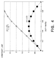
- a voltage waveform Vds1' of the first switching element Q1 is illustrated by a rectangle waveform having an amplitude voltage equal to Vin.
- Vds1'(x) Vin ⁇ D + 2 ⁇ (-sinD ⁇ cosx + 1 2 sin2D ⁇ cos2x - 1 3 sin3D ⁇ cos3x + ...) ⁇ .
- varies in the form of a sine wave to the duty ratio D
- varies nonlinearly to the variation of the duty ratio D when the duty ratio D is within the range of 0.2-0.5.
- has a little variation even if the duty ratio D has the variation as shown by dotted line in Fig. 4.
- the duty ratio D is smaller than 0.2, a switching loss increases because a switching pulse width is too narrow. As a result, the resonant DC-DC converter has a degraded efficiency. Under the circumstances, the duty ratio D is practically determined at a variable range of 0.2-0.5. This means that it is impossible to control the resonant DC-DC converter by PWM (pulse width modulation) control by the use of the duty ratio D.
- an oscillation frequency fs changes from 60 (kHz) to 90 (kHz) (1.5 times) when the input voltage Vin changes from 80 (V) to 130 (V) (1.6 times).
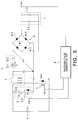
- the resonant DC-DC converter comprises a d.c. power source 1 having an input voltage Vin, a clamp circuit 2 connected to the d.c. power source 1, a main switching element 3 connected to the d.c. power source 1 and the clamp circuit 2, and a transformer 4.
- the clamp circuit 2 comprises a first capacitor 2-1 and an auxiliary switching element 2-2 serially connected to the first capacitor 2-1.
- the clamp circuit 2 is connected in parallel to a primary side, namely, a primary coil, of the transformer 4 while the main switching element 3 is serially connected to the primary side of the transformer 4.
- the main and the auxiliary switching elements 3 and 2-2 are alternately put into an on state under control of first and second switching pulses, namely, gate pulses, Vg1 and Vg2.
- first and second switching pulses namely, gate pulses, Vg1 and Vg2.
- the main and the auxiliary switching elements 3 and 2-2 carry out switching operation of the input voltage Vin.
- the resonant DC-DC converter further comprises a series resonant circuit 5 serially connected to a secondary side, namely, a secondary coil, of the transformer 4, a full wave rectifier circuit 6 of a bridge type, and a smoothing circuit 7 of a capacitor input type.
- the series resonant circuit 5 comprises a first inductor 5-1 and a second capacitor 5-2 serially connected to the first inductor 5-1.
- the full wave rectifier circuit 6 is for rectifying an output of the series resonant circuit 5 and comprises first through fourth diodes 6-1, 6-2, 6-3, and 6-4.
- the smoothing circuit 7 is for smoothing an output of the full wave rectifier circuit 6 to produce a d.c. output voltage Vout and comprises a capacitor 7-1 and a load resistor 7-2.
- a switching pulse generation circuit 8 is for generating the first and the second switching pulses Vg1 and Vg2 in response to the d.c. output voltage Vout.
- each of the main and the auxiliary switching elements 3 and 2-2 is implemented by an nMOSFET having an integrated body diode. This is applied to all embodiments which will be described later.
- the main and the auxiliary switching elements 3 and 2-2 are put into the on state with the main and the auxiliary switching elements 3 and 2-2 having a dead time.
- Soft switching operation is carried out during each dead time of the main and the auxiliary switching elements 3 and 2-2.
- an output capacitor of each switching element is charged and discharged by an magnetizing current of primary side of the transformer 4 through the integrated body diode.
- a third equation (3) is led from voltage time product balance of an inductor in the primary side of the transformer 4 by using a terminal voltage Vc of the first capacitor 2-1 and a duty ratio D.
- VinD Vc(1 - D).
- Vc D 1 - D Vin.
- Vds1 Vin 1 - D ⁇ D + 2 ⁇ (sinD ⁇ cosx + 1 2 sin2D ⁇ cos2x - 1 3 sin3D ⁇ cos3x + ... ) ⁇ .
- Vds1ac varies linearly to the variation of the duty ratio D when the duty ratio D is in a range of 0.2-0.8 that is a practical variable range. This fact is illustrated in Fig. 4 by a real line.
- the resonant DC-DC converter according to this invention can be controlled by the PWM control at a constant frequency.
- the terminal voltage Vds1 is converted by the transformer 4 into an a.c. voltage Vs.
- the a.c. voltage Vs is supplied to the full wave rectifier circuit 6 through the series resonant circuit 5 and rectified into a rectified voltage.
- the smoothing circuit 7 smooths the rectified voltage and delivers a smoothed voltage as the d.c. output voltage Vout.
- a current Ir flowing through the series resonant circuit 5 is a fundamental wave, namely, a sine wave as illustrated in Fig. 6.
- the switching pulse generation circuit 8 comprises an error amplifier 8-1, a PWM control unit 8-2, and a drive circuit 8-3.
- the error amplifier 8-1 is supplied with a reference voltage Vref and supplied with the d.c. output voltage Vout from the smoothing circuit 7.
- the error amplifier 8-1 amplifies a difference between the reference voltage Vref and the d.c. output voltage Vout and produces an amplified error voltage.
- the PWM control unit 8-2 modulates the duty ratio D in response to the amplified error voltage and delivers a duty ratio modulated signal having a modulated duty ratio to the drive circuit 8-3.
- the drive circuit 8-3 generates first and second pulses which have a constant frequency and which have a pulse width corresponding to the modulated duty ratio.
- the drive circuit 8-3 supplies the first and the second pulses to the main and the auxiliary switching elements 3 and 2-2 as the first and the second switching pulses Vg1 and Vg2, respectively.
- Such a first example is suitable for a case that input fluctuation and load fluctuation are not so large.
- the switching pulse generation circuit 8 comprises the error amplifier 8-1, a PWM control unit 8-2', a drive circuit 8-3', and a V/f (voltage/frequency) converter 8-4.
- the error amplifier 8-1 produces the amplified error voltage.
- the V/f converter 8-4 converts the amplified error voltage into a variable frequency signal having a frequency which varies with the amplified error voltage.
- the PWM control unit 8-2' modulates the duty ratio D in response to the input voltage Vin and delivers a duty ratio modulated signal having a modulated duty ratio to the drive circuit 8-3'.
- the drive circuit 8-3' generates first and second pulses which have a frequency corresponding to the frequency of the variable frequency signal and which have a pulse width corresponding to the modulated duty ratio.
- the drive circuit 8-3' supplies the first and the second pulses to the main and the auxiliary switching elements 3 and 2-2 as the first and the second switching pulses Vg1 and Vg2, respectively.
- Such a second example is suitable for a case that it has large input fluctuation and large load fluctuation. Namely, the frequency control is utilized for load fluctuation while the PWM control is utilized for input fluctuation.
- a resonant DC-DC converter according to a second embodiment of this invention.
- the resonant DC-DC converter is similar to that illustrated in Fig. 5 except that a transformer 4' is a type having a center tap 4-1 and that the series resonant circuit 5 is connected to the center tap 4-1.
- a full wave rectifier circuit 9 comprising first and second diodes 9-1 and 9-2 is used in place of the full wave rectifier circuit 6 shown in Fig. 5.
- the full wave rectifier circuit 9 rectifies an output of the series resonant circuit 5 and supplies the rectified voltage to the smoothing circuit 7. Operation of remaining parts is similar to that described in conjunction with Figs. 5 and 6.
- the resonant DC-DC converter is similar to that illustrated in Fig. 9 except that a synchronous rectifier circuit 10 is used in place of the full wave rectifier circuit 9.
- the synchronous rectifier circuit 10 comprises first and second nMOSFETs 10-1 and 10-2. Namely, each of the first and the second nMOSFETs 10-1 and 10-2 has an integrated body diode. Operation is similar to that illustrated in Fig. 9.
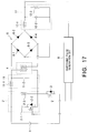
- the resonant DC-DC converter is similar to that illustrated in Fig. 5 except that a parallel resonant circuit 11 is used in place of the series resonant circuit 5 and that a smoothing circuit 12 of a choke input type is used in place of the smoothing circuit 7.
- the parallel resonant circuit 11 comprises a first inductor 11-1 and a second capacitor 11-2.
- the smoothing circuit 12 comprises a choke coil 12-1, a capacitor 12-2, and a load resistor 12-3.
- the full wave rectifier circuit 6 rectifies an output of the parallel resonant circuit 11 and supplies the rectified voltage to the smoothing circuit 12.
- the smoothing circuit 12 smooths the rectified voltage and produces a smoothed voltage as the d.c. output voltage Vout. Operation of remaining parts is similar to that described in conjunction with Figs. 5 and 6.
- a resonant DC-DC converter according to a fifth embodiment of this invention.
- the resonant DC-DC converter is similar to that illustrated in Fig. 9 except that the parallel resonant circuit 11 mentioned in Fig. 11 is used in place of the series resonant circuit 5 and that the smoothing circuit 12 described in Fig. 11 is used in place of the smoothing circuit 7 of the capacitor input type. Operation of the resonant DC-DC converter is similar to that described in conjunction with Figs. 5 and 6.
- a resonant DC-DC converter according to a sixth embodiment of this invention is similar to that illustrated in Fig. 10 except that the parallel resonant circuit 11 mentioned in Fig. 11 is used in place of the series resonant circuit 5 and that the smoothing circuit 12 described in Fig. 11 is used in place of the smoothing circuit 7 of the capacitor input type. Operation of the resonant DC-DC converter is similar to that described in conjunction with Figs. 5 and 6.
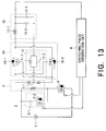
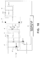
- a resonant DC-DC converter according to a seventh embodiment of this invention is similar to that illustrated in Fig. 5 except that a clamp circuit 2' is used in place of the clamp circuit 2 and that the series resonant circuit 5 is removed from the secondary side of the transformer 4 and is connected between the clamp circuit 2' and the primary side of the transformer 4.
- the clamp circuit 2' comprises the first capacitor 2-1, the auxiliary switching element 2-2, and a third inductor 2-3 which is connected in parallel to the first capacitor 2-1 and the auxiliary switching element 2-2. Operation of the resonant DC-DC converter is similar to that described in relation to Figs. 5 and 6.
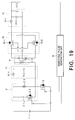
- a resonant DC-DC converter according to an eighth embodiment of this invention is similar to that illustrated in Fig. 14 except that the transformer 4' having the center tap 4-1 is used in place of the transformer 4 and that the full wave rectifier circuit 9 is used in place of the full wave rectifier circuit 6. Operation of the resonant DC-DC converter is similar to that described in conjunction with Figs. 5 and 6.
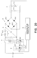
- a resonant DC-DC converter according to a ninth embodiment of this invention is similar to that illustrated in Fig. 14 except that the synchronous rectifier circuit 10 is used in place the full wave rectifier circuit 9. Operation of the resonant DC-DC converter is similar to that described in conjunction with Figs. 5 and 6.
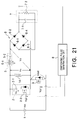
- a resonant DC-DC converter according to a tenth embodiment of this invention is similar to that illustrated in Fig. 14 except that the parallel resonant circuit 11 is used in place of the series resonant circuit 5 and that the smoothing circuit 12 of the choke input type is used in place of the smoothing circuit 7 of the capacitor input type. Operation of the resonant DC-DC converter is similar to that described in conjunction with Figs. 5 and 6.
- a resonant DC-DC converter according to an eleventh embodiment of this invention is similar to that illustrated in Fig. 15 except that the parallel resonant circuit 11 is used in place of the series resonant circuit 5 and that the smoothing circuit 12 of the choke input type is used in place of the smoothing circuit 7 of the capacitor input type. Operation of the resonant DC-DC converter is similar to that described in conjunction with Figs. 5 and 6.
- a resonant DC-DC converter according to a twelfth embodiment of this invention is similar to that illustrated in Fig. 18 except that the synchronous rectifier circuit 10 is used in place of the full wave rectifier circuit 9. Operation of the resonant DC-DC converter is similar to that described in conjunction with Figs. 5 and 6.
- auxiliary switching element 2-2' is used in place of the auxiliary switching element 2-2.
- the auxiliary switching element 2-2' is implemented by a pMOSFET having an integrated body diode.
- the clamp circuit 2-2' is connected in parallel to the main switching element 3. Operation of the resonant DC-DC converter is similar to that described in conjunction with Figs. 5 and 6. Such a modification can be applied to all embodiments which are described hereinbefore.
- a resonant DC-DC converter illustrated in Fig. 22 is a modification of the resonant DC-DC converter of the fourth embodiment illustrated in Fig. 11.
- the auxiliary switching element 2-2 may be implemented by the pMOSFET.
- the transformer may be removed.
- circuit elements connected to the primary side are directly connected to circuit elements connected to the secondary side.
- the resonant DC-DC converter is the modification of the seventh embodiment illustrated in Fig. 14.
- the clamp circuit 2' and the series resonant circuit 5 are directly connected to the full wave rectifier circuit 6.
- the resonant DC-DC converter is the modification of the tenth embodiment illustrated in Fig. 17.
- the parallel resonant circuit 11 is directly connected to the full wave rectifier circuit 6.
- the auxiliary switching element 2-2 may be implemented by the pMOSFET.
- a measurement result which is applied to the first embodiment illustrated in Fig. 5.
- the measurement is carried out under a condition that a switching frequency is constant at 200 (kHz).
- the input voltage Vin varies in a range of 35-70 (V) and the duty ratio D varies so that the d.c. output voltage and the output current become equal to 9 (V) and 5 (A), respectively.
- the d.c. output voltage can be controlled at a constant by changing the duty ratio D under the condition of a constant switching frequency. It is possible to obtain efficiency of 80 (%) or over.
- Fig. 26 shows waveforms of the voltages Vds1, Vs, and Vd and the current Ir which are illustrated in Fig. 5 under a condition that the input voltage Vin is equal to 48 (V), the d.c. output voltage is equal to 9 (V), the output current is equal to 5 (A), and the duty ratio D is equal to 0.5.
- Fig. 27 shows a relation between the duty ratio D and the efficiency when the output current varies in a range between 1 and 5 (A) at a constant d.c. output voltage of 9 (V). As apparent from Fig. 27, it is possible to hold the d.c. output voltage at a constant value of 9 (V) without a large change of the duty ratio D, if the load fluctuation occurs.
Landscapes
- Engineering & Computer Science (AREA)
- Power Engineering (AREA)
- Dc-Dc Converters (AREA)
Applications Claiming Priority (2)
| Application Number | Priority Date | Filing Date | Title |
|---|---|---|---|
| JP7247525A JP2792536B2 (ja) | 1995-09-26 | 1995-09-26 | 共振型dc−dcコンバータ |
| JP247525/95 | 1995-09-26 |
Publications (2)
| Publication Number | Publication Date |
|---|---|
| EP0766372A2 true EP0766372A2 (fr) | 1997-04-02 |
| EP0766372A3 EP0766372A3 (fr) | 1998-08-26 |
Family
ID=17164798
Family Applications (1)
| Application Number | Title | Priority Date | Filing Date |
|---|---|---|---|
| EP96106757A Withdrawn EP0766372A3 (fr) | 1995-09-26 | 1996-04-29 | Convertisseur résonant courant continu-courant continu contrÔlable par modulation de largeur d'impulsion |
Country Status (3)
| Country | Link |
|---|---|
| US (1) | US5805432A (fr) |
| EP (1) | EP0766372A3 (fr) |
| JP (1) | JP2792536B2 (fr) |
Cited By (3)
| Publication number | Priority date | Publication date | Assignee | Title |
|---|---|---|---|---|
| WO2000059104A1 (fr) * | 1999-03-26 | 2000-10-05 | Sarnoff Corporation | Alimentation d'energie a commutation souple et a haute performance |
| EP1156580A3 (fr) * | 2000-05-17 | 2004-01-14 | Sony Corporation | Appareil d'alimentation de puisance à découpage |
| EP1727265A4 (fr) * | 2004-03-18 | 2009-02-18 | Mitsui Bussan | Convertisseur cc-cc |
Families Citing this family (36)
| Publication number | Priority date | Publication date | Assignee | Title |
|---|---|---|---|---|
| US5781420A (en) * | 1996-07-18 | 1998-07-14 | International Power Devices, Inc. | Single ended forward DC-to-DC converter providing enhanced resetting for synchronous rectification |
| EP0954899A2 (fr) | 1997-01-24 | 1999-11-10 | Fische, LLC | Convertisseur de puissance a haute efficacite |
| US7269034B2 (en) | 1997-01-24 | 2007-09-11 | Synqor, Inc. | High efficiency power converter |
| JPH11164554A (ja) * | 1997-11-28 | 1999-06-18 | Toshiba Corp | 電流共振電源回路 |
| US6005782A (en) * | 1998-10-16 | 1999-12-21 | Nortel Networks Corporation | Flyback converter with soft switching using auxiliary switch and resonant circuit |
| US6147886A (en) * | 1999-05-15 | 2000-11-14 | Technical Witts, Inc. | Dual opposed interleaved coupled inductor soft switching converters |
| US6272023B1 (en) * | 1999-05-15 | 2001-08-07 | Technical Witts, Inc | High efficiency coupled inductor soft switching power converters |
| US6246592B1 (en) | 1999-08-10 | 2001-06-12 | Texas Instruments Incorporated | Unique power supply architecture with cascaded converters for large input-to-output step-down ratio |
| US6169683B1 (en) * | 1999-10-07 | 2001-01-02 | Ericsson Inc. | Resonant gate drive for synchronous rectifiers |
| JP3475926B2 (ja) * | 2000-10-11 | 2003-12-10 | 株式会社村田製作所 | スイッチング電源装置 |
| US6344979B1 (en) * | 2001-02-09 | 2002-02-05 | Delta Electronics, Inc. | LLC series resonant DC-to-DC converter |
| US6650552B2 (en) * | 2001-05-25 | 2003-11-18 | Tdk Corporation | Switching power supply unit with series connected converter circuits |
| US6975098B2 (en) * | 2002-01-31 | 2005-12-13 | Vlt, Inc. | Factorized power architecture with point of load sine amplitude converters |
| US6930893B2 (en) * | 2002-01-31 | 2005-08-16 | Vlt, Inc. | Factorized power architecture with point of load sine amplitude converters |
| JP4542844B2 (ja) * | 2003-07-16 | 2010-09-15 | 株式会社日本自動車部品総合研究所 | 2トランス型dc−dcコンバータ |
| JP3664173B2 (ja) * | 2003-11-17 | 2005-06-22 | サンケン電気株式会社 | 直流変換装置 |
| US20050286191A1 (en) * | 2004-06-28 | 2005-12-29 | Pieter Vorenkamp | Power supply integrated circuit with multiple independent outputs |
| JP2006191746A (ja) * | 2005-01-06 | 2006-07-20 | Sony Corp | スイッチング電源回路 |
| TWI313102B (en) * | 2005-02-21 | 2009-08-01 | Delta Electronics Inc | Llc series resonant converter and the driving method of the synchronous rectifier power switches thereof |
| JP2006254540A (ja) * | 2005-03-08 | 2006-09-21 | Sony Corp | スイッチング電源回路 |
| TW200723660A (en) * | 2005-09-30 | 2007-06-16 | Sony Corp | Switching power supply circuit |
| TWI314808B (en) * | 2006-09-06 | 2009-09-11 | Delta Electronics Inc | Resonance converter and driving method for synchronous rectifier thereof |
| JP2008131793A (ja) * | 2006-11-22 | 2008-06-05 | Sanken Electric Co Ltd | 直流変換装置 |
| US8199529B2 (en) * | 2008-09-04 | 2012-06-12 | Astec International Limited | Inductorless isolated power converters with zero voltage and zero current switching |
| US8339810B2 (en) * | 2010-03-12 | 2012-12-25 | Illinois Tool Works Inc. | Wide input voltage power supply |
| CN102299633B (zh) * | 2010-06-24 | 2015-07-08 | 英飞特电子(杭州)股份有限公司 | 一种dc-dc变换电路 |
| US9030850B2 (en) | 2011-07-07 | 2015-05-12 | Fuji Electric Co., Ltd. | Resonant switching regulator with adaptive dead time |
| JP5556859B2 (ja) * | 2012-07-03 | 2014-07-23 | Tdk株式会社 | 電流共振型dcdcコンバータ |
| JP6167643B2 (ja) * | 2013-04-25 | 2017-07-26 | 株式会社リコー | 電源装置、画像形成装置及び電子機器 |
| US10199950B1 (en) | 2013-07-02 | 2019-02-05 | Vlt, Inc. | Power distribution architecture with series-connected bus converter |
| US9991800B2 (en) * | 2015-05-20 | 2018-06-05 | Semiconductor Components Industries, Llc | Switched mode power supply with efficient operation at light loads and method therefor |
| JP7003445B2 (ja) * | 2017-05-19 | 2022-02-04 | オムロン株式会社 | 非接触給電装置 |
| JP6399244B1 (ja) * | 2017-06-02 | 2018-10-03 | オムロン株式会社 | 非接触給電装置及び異常停止方法 |
| US10298138B2 (en) | 2017-08-31 | 2019-05-21 | Google Llc | Programmable power adapter |
| US10277140B2 (en) | 2017-08-31 | 2019-04-30 | Google Llc | High-bandwith resonant power converters |
| IL255948A (en) * | 2017-11-27 | 2018-01-31 | Abramovici Tal | Direct current / constant frequency direct current converter |
Family Cites Families (18)
| Publication number | Priority date | Publication date | Assignee | Title |
|---|---|---|---|---|
| JPS5378042A (en) * | 1976-12-20 | 1978-07-11 | Sanyo Electric Co Ltd | Switching control type power source circuit |
| JPS5858866A (ja) * | 1981-10-05 | 1983-04-07 | Toshiba Corp | スイッチング装置 |
| BE1001220A6 (nl) * | 1987-11-16 | 1989-08-22 | Bell Telephone Mfg Company N V | Electrische omvormer. |
| JP2773195B2 (ja) * | 1988-04-05 | 1998-07-09 | 松下電器産業株式会社 | スイッチング電源装置 |
| US4926304A (en) * | 1988-06-30 | 1990-05-15 | U.S. Philips Corporation | Switched-mode power supply with low loss interrupted oscillation |
| JPH0297272A (ja) * | 1988-09-30 | 1990-04-09 | Fujitsu Ltd | 一石式共振形コンバータ |
| JP2732624B2 (ja) * | 1988-11-30 | 1998-03-30 | 株式会社東芝 | 並列共振コンバータ |
| US5066900A (en) * | 1989-11-14 | 1991-11-19 | Computer Products, Inc. | Dc/dc converter switching at zero voltage |
| JPH04217863A (ja) * | 1990-01-31 | 1992-08-07 | Toshiba Corp | 電流共振コンバータ |
| JP3024165B2 (ja) * | 1990-05-25 | 2000-03-21 | 松下電器産業株式会社 | 磁気記録再生装置 |
| JPH04359671A (ja) * | 1991-02-22 | 1992-12-11 | Murata Mfg Co Ltd | 電圧共振型dc−dcコンバータ |
| US5343079A (en) * | 1991-02-25 | 1994-08-30 | Regents Of The University Of Minnesota | Standby power supply with load-current harmonics neutralizer |
| JPH0556638A (ja) * | 1991-08-27 | 1993-03-05 | Sanken Electric Co Ltd | スイツチング電源装置 |
| US5159541A (en) * | 1991-10-31 | 1992-10-27 | Northern Telecom Limited | Asymmetrical pulse width modulated resonant DC/DC converter |
| DE4313359A1 (de) * | 1992-04-24 | 1993-10-28 | Matsushita Electric Industrial Co Ltd | Schaltnetzteil |
| US5430633A (en) * | 1993-09-14 | 1995-07-04 | Astec International, Ltd. | Multi-resonant clamped flyback converter |
| JP3214679B2 (ja) * | 1993-09-14 | 2001-10-02 | オリジン電気株式会社 | 直列共振コンバータ |
| US5434767A (en) * | 1994-01-10 | 1995-07-18 | University Of Central Florida | Power converter possessing zero-voltage switching and output isolation |
-
1995
- 1995-09-26 JP JP7247525A patent/JP2792536B2/ja not_active Expired - Fee Related
-
1996
- 1996-04-25 US US08/637,368 patent/US5805432A/en not_active Expired - Lifetime
- 1996-04-29 EP EP96106757A patent/EP0766372A3/fr not_active Withdrawn
Cited By (4)
| Publication number | Priority date | Publication date | Assignee | Title |
|---|---|---|---|---|
| WO2000059104A1 (fr) * | 1999-03-26 | 2000-10-05 | Sarnoff Corporation | Alimentation d'energie a commutation souple et a haute performance |
| US6359795B1 (en) | 1999-03-26 | 2002-03-19 | Sarnoff Corporation | Soft-switching power supply with auxiliary resonator |
| EP1156580A3 (fr) * | 2000-05-17 | 2004-01-14 | Sony Corporation | Appareil d'alimentation de puisance à découpage |
| EP1727265A4 (fr) * | 2004-03-18 | 2009-02-18 | Mitsui Bussan | Convertisseur cc-cc |
Also Published As
| Publication number | Publication date |
|---|---|
| EP0766372A3 (fr) | 1998-08-26 |
| JPH0993922A (ja) | 1997-04-04 |
| JP2792536B2 (ja) | 1998-09-03 |
| US5805432A (en) | 1998-09-08 |
Similar Documents
| Publication | Publication Date | Title |
|---|---|---|
| US5805432A (en) | Resonant DC-DC converter capable of controlling by pulse width modulation | |
| US6370039B1 (en) | Isolated power converter having primary feedback control | |
| US7208883B2 (en) | Current detection circuit, and power supply apparatus, power supply system and electronic apparatus using the current detection circuit | |
| US5519306A (en) | Constant voltage circuit and a stabilized power supply unit | |
| US6385059B1 (en) | Transformer-coupled switching power converter having primary feedback control | |
| US6381150B2 (en) | Isolated dual converter having primary side internal feedback for output regulation | |
| US4126891A (en) | Switching regulator with feedback system for regulating output current | |
| US6943538B2 (en) | Apparatus for and method of measuring power consumption | |
| US4502104A (en) | Bootstrapped AC-DC power converter | |
| GB2253311A (en) | Power factor correction converter | |
| US4439821A (en) | DC to DC switching regulator with temperature compensated isolated feedback circuitry | |
| US4943903A (en) | Power supply in which regulation is achieved by processing a small portion of applied power through a switching regulator | |
| US20040252532A1 (en) | Power supply apparatus | |
| US5777503A (en) | Pulse width modulation bias to minimize effect of noise due to ramp switching | |
| US4176392A (en) | Series induction/parallel inverter power stage and power staging method for DC-DC power converter | |
| JP2817670B2 (ja) | 広入力圧電トランスインバータ | |
| US4352055A (en) | AC Variable voltage source utilizing pulse width modulation | |
| JPH0449846A (ja) | 圧電トランスdc/dcコンバータ | |
| US5572413A (en) | Primary control type switching power supply circuit | |
| US20070133232A1 (en) | Technique to improve dynamic response of two-stage converters | |
| JPH04261358A (ja) | スイッチング電源装置 | |
| JPH01157270A (ja) | スイッチング電源装置 | |
| JP2604302Y2 (ja) | 共振形dc−dcコンバータ | |
| JPH04265A (ja) | 電力変換装置 | |
| JPH0537669Y2 (fr) |
Legal Events
| Date | Code | Title | Description |
|---|---|---|---|
| PUAI | Public reference made under article 153(3) epc to a published international application that has entered the european phase |
Free format text: ORIGINAL CODE: 0009012 |
|
| AK | Designated contracting states |
Kind code of ref document: A2 Designated state(s): DE FR GB |
|
| PUAL | Search report despatched |
Free format text: ORIGINAL CODE: 0009013 |
|
| AK | Designated contracting states |
Kind code of ref document: A3 Designated state(s): DE FR GB |
|
| 17P | Request for examination filed |
Effective date: 19981228 |
|
| 17Q | First examination report despatched |
Effective date: 20030205 |
|
| STAA | Information on the status of an ep patent application or granted ep patent |
Free format text: STATUS: THE APPLICATION HAS BEEN WITHDRAWN |
|
| 18W | Application withdrawn |
Effective date: 20030505 |