EP0766863B1 - Verfahren zum lesen von informationen - Google Patents
Verfahren zum lesen von informationen Download PDFInfo
- Publication number
- EP0766863B1 EP0766863B1 EP96915061A EP96915061A EP0766863B1 EP 0766863 B1 EP0766863 B1 EP 0766863B1 EP 96915061 A EP96915061 A EP 96915061A EP 96915061 A EP96915061 A EP 96915061A EP 0766863 B1 EP0766863 B1 EP 0766863B1
- Authority
- EP
- European Patent Office
- Prior art keywords
- sam
- sample
- reading
- samples
- read
- Prior art date
- Legal status (The legal status is an assumption and is not a legal conclusion. Google has not performed a legal analysis and makes no representation as to the accuracy of the status listed.)
- Expired - Lifetime
Links
- 238000000034 method Methods 0.000 title claims description 14
- 238000010200 validation analysis Methods 0.000 claims description 23
- 230000008569 process Effects 0.000 claims description 10
- 238000005070 sampling Methods 0.000 claims description 7
- BRLQWZUYTZBJKN-UHFFFAOYSA-N Epichlorohydrin Chemical compound ClCC1CO1 BRLQWZUYTZBJKN-UHFFFAOYSA-N 0.000 description 36
- 238000004364 calculation method Methods 0.000 description 7
- 230000006870 function Effects 0.000 description 6
- 238000010586 diagram Methods 0.000 description 5
- 239000000758 substrate Substances 0.000 description 5
- 230000005693 optoelectronics Effects 0.000 description 4
- 230000004888 barrier function Effects 0.000 description 3
- 230000008901 benefit Effects 0.000 description 3
- 239000011159 matrix material Substances 0.000 description 3
- 230000008929 regeneration Effects 0.000 description 3
- 238000011069 regeneration method Methods 0.000 description 3
- 230000005540 biological transmission Effects 0.000 description 2
- 239000004020 conductor Substances 0.000 description 2
- 238000009413 insulation Methods 0.000 description 2
- 238000012544 monitoring process Methods 0.000 description 2
- 230000003287 optical effect Effects 0.000 description 2
- 230000010287 polarization Effects 0.000 description 2
- 230000005374 Kerr effect Effects 0.000 description 1
- 230000001133 acceleration Effects 0.000 description 1
- 230000009471 action Effects 0.000 description 1
- 230000005684 electric field Effects 0.000 description 1
- 238000002955 isolation Methods 0.000 description 1
- 238000005457 optimization Methods 0.000 description 1
- 230000002093 peripheral effect Effects 0.000 description 1
- 230000036316 preload Effects 0.000 description 1
- 230000000717 retained effect Effects 0.000 description 1
- 230000033764 rhythmic process Effects 0.000 description 1
- 230000001360 synchronised effect Effects 0.000 description 1
- 230000007704 transition Effects 0.000 description 1
Images


Classifications
-
- G—PHYSICS
- G11—INFORMATION STORAGE
- G11B—INFORMATION STORAGE BASED ON RELATIVE MOVEMENT BETWEEN RECORD CARRIER AND TRANSDUCER
- G11B11/00—Recording on or reproducing from the same record carrier wherein for these two operations the methods are covered by different main groups of groups G11B3/00 - G11B7/00 or by different subgroups of group G11B9/00; Record carriers therefor
- G11B11/10—Recording on or reproducing from the same record carrier wherein for these two operations the methods are covered by different main groups of groups G11B3/00 - G11B7/00 or by different subgroups of group G11B9/00; Record carriers therefor using recording by magnetic means or other means for magnetisation or demagnetisation of a record carrier, e.g. light induced spin magnetisation; Demagnetisation by thermal or stress means in the presence or not of an orienting magnetic field
- G11B11/105—Recording on or reproducing from the same record carrier wherein for these two operations the methods are covered by different main groups of groups G11B3/00 - G11B7/00 or by different subgroups of group G11B9/00; Record carriers therefor using recording by magnetic means or other means for magnetisation or demagnetisation of a record carrier, e.g. light induced spin magnetisation; Demagnetisation by thermal or stress means in the presence or not of an orienting magnetic field using a beam of light or a magnetic field for recording by change of magnetisation and a beam of light for reproducing, i.e. magneto-optical, e.g. light-induced thermomagnetic recording, spin magnetisation recording, Kerr or Faraday effect reproducing
- G11B11/10502—Recording on or reproducing from the same record carrier wherein for these two operations the methods are covered by different main groups of groups G11B3/00 - G11B7/00 or by different subgroups of group G11B9/00; Record carriers therefor using recording by magnetic means or other means for magnetisation or demagnetisation of a record carrier, e.g. light induced spin magnetisation; Demagnetisation by thermal or stress means in the presence or not of an orienting magnetic field using a beam of light or a magnetic field for recording by change of magnetisation and a beam of light for reproducing, i.e. magneto-optical, e.g. light-induced thermomagnetic recording, spin magnetisation recording, Kerr or Faraday effect reproducing characterised by the transducing operation to be executed
- G11B11/10515—Reproducing
-
- G—PHYSICS
- G11—INFORMATION STORAGE
- G11B—INFORMATION STORAGE BASED ON RELATIVE MOVEMENT BETWEEN RECORD CARRIER AND TRANSDUCER
- G11B11/00—Recording on or reproducing from the same record carrier wherein for these two operations the methods are covered by different main groups of groups G11B3/00 - G11B7/00 or by different subgroups of group G11B9/00; Record carriers therefor
- G11B11/10—Recording on or reproducing from the same record carrier wherein for these two operations the methods are covered by different main groups of groups G11B3/00 - G11B7/00 or by different subgroups of group G11B9/00; Record carriers therefor using recording by magnetic means or other means for magnetisation or demagnetisation of a record carrier, e.g. light induced spin magnetisation; Demagnetisation by thermal or stress means in the presence or not of an orienting magnetic field
- G11B11/105—Recording on or reproducing from the same record carrier wherein for these two operations the methods are covered by different main groups of groups G11B3/00 - G11B7/00 or by different subgroups of group G11B9/00; Record carriers therefor using recording by magnetic means or other means for magnetisation or demagnetisation of a record carrier, e.g. light induced spin magnetisation; Demagnetisation by thermal or stress means in the presence or not of an orienting magnetic field using a beam of light or a magnetic field for recording by change of magnetisation and a beam of light for reproducing, i.e. magneto-optical, e.g. light-induced thermomagnetic recording, spin magnetisation recording, Kerr or Faraday effect reproducing
- G11B11/10532—Heads
- G11B11/10541—Heads for reproducing
- G11B11/10543—Heads for reproducing using optical beam of radiation
- G11B11/10547—Heads for reproducing using optical beam of radiation interacting with the magnetisation of an intermediate transfer element, e.g. magnetic film, included in the head
-
- G—PHYSICS
- G11—INFORMATION STORAGE
- G11B—INFORMATION STORAGE BASED ON RELATIVE MOVEMENT BETWEEN RECORD CARRIER AND TRANSDUCER
- G11B20/00—Signal processing not specific to the method of recording or reproducing; Circuits therefor
- G11B20/10—Digital recording or reproducing
- G11B20/10527—Audio or video recording; Data buffering arrangements
-
- G—PHYSICS
- G11—INFORMATION STORAGE
- G11B—INFORMATION STORAGE BASED ON RELATIVE MOVEMENT BETWEEN RECORD CARRIER AND TRANSDUCER
- G11B5/00—Recording by magnetisation or demagnetisation of a record carrier; Reproducing by magnetic means; Record carriers therefor
- G11B5/48—Disposition or mounting of heads or head supports relative to record carriers ; arrangements of heads, e.g. for scanning the record carrier to increase the relative speed
- G11B5/49—Fixed mounting or arrangements, e.g. one head per track
- G11B5/4969—Details for track selection or addressing
-
- G—PHYSICS
- G11—INFORMATION STORAGE
- G11B—INFORMATION STORAGE BASED ON RELATIVE MOVEMENT BETWEEN RECORD CARRIER AND TRANSDUCER
- G11B20/00—Signal processing not specific to the method of recording or reproducing; Circuits therefor
- G11B20/20—Signal processing not specific to the method of recording or reproducing; Circuits therefor for correction of skew for multitrack recording
Definitions
- a method of reading media recording device and a device applying such a method is a method of reading media recording device and a device applying such a method.
- the invention is particularly applicable to the reading of recordings magnetic or optical and, more particularly, reading high density recordings. It finds a preferential application in recording systems such as peripherals IT and all professional systems.
- VCO Voltage Controlled Oscillator
- PLL Phase Locked Loop
- the invention does not have these drawbacks.
- An advantage of the invention is to avoid the multiplication of clock regeneration circuits and decoding circuits for binary information.
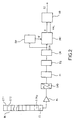
- Figure 1 shows an example of a system recording / playback to which the invention applies.
- the recording is done with a matrix head and reading with a magneto-optical system.
- the invention relates to other systems recording / playback.
- the support on which the information is recorded may not be a magnetic medium but can be an optical medium. It can be in the form of a disc and not of a band.
- Reading can be carried out by any known means other than a light beam, for example by a multitrack head with magneto-resistive elements.
- the system described in Figure 1 includes a support recording tape such as BD tape.
- a head MT1 matrix recording system has a head matrix elementary MT2 controlled by line selection conductors MT3 and MT4 data selection conductors. This head allows to record on the BD tape different information tracks p1, p2, ... pX.
- This TL head comprises a TL1 magneto-optical transducer, by example with Kerr effect, arranged parallel to the plane of the magnetic strip and the great length of which is transverse to the length of the strip.
- a light source TL2 illuminates with a beam of polarized light and through a TL3 focusing system, the TL1 transducer in such a way that the light beam is focused substantially along a line on a face of the TL1 transducer near the BD magnetic strip.
- the beam reflected by the TL1 transducer has its polarization changed to function of the magnetic field on the tape.
- the reflected beam is transmitted by a TL4 focusing system and a tracking system TL5 to a TL6 optoelectronic detector.
- the TL6 detector is a device charge transfer photosensitive consisting of a photosensitive zone and a non-photosensitive area.
- the photosensitive area is then preferably consisting of a linear array of Np pixels and the area non-photosensitive of a reading register consisting of transfer stages.
- the charges generated in a pixel of the photosensitive area are collected in a transfer stage of the reading register.
- the detector TL6 has at least as many pixels as there are tracks on the tape.
- the TL1 transducer reflects a beam towards the TL6 detector actually made up of a set of track reading beams, each having had its polarization influenced by a track of the magnetic strip. All of these reading beams are received by the TL6 detector which thus makes it possible to detect the information read on each track of the strip BD.
- the information read may have been saved at the same time. It can also be information recorded in a time-shifted manner. Preferably, the information read is sampled at a frequency F e greater than the frequency Fbit with which it was written on the tape BD.
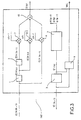
- FIG. 2 represents a block diagram of the principle of device of the invention.
- the reading register RL of the detector TL6 has been shown in FIG. 2.
- the reading register RL consists of a succession of N p transfer stages ET1, ET2, ...., ETNp .
- the output circuit CS of the read register consists of a charge-voltage converter comprising a read diode and a first read amplifier not shown in the figure.
- the signal from the CS output circuit consists of a train serial information.
- the signal from the CS output passes successively through a second amplifier AL reading, an analog-digital CAD converter, a high-pass IF filter, an EQ equalizer and a CR corrector.
- the CR corrector is a circuit correcting the crosstalk existing between a pixel and the two neighboring pixels surrounding this pixel.
- the CR corrector can be, for example, such as that described in the patent application filed in France on behalf of Plaintiffs on December 22, 1992 and registered under number 92 15474.
- the information read simultaneously by the TL1 transducer are the same information rank k contained on the X parallel tracks.
- Digital operators such that the high-pass filter FI, the equalizer EQ and the corrector CR, have then as many delay circuits as necessary so that the successive samples they process represent the information successive of the same track.
- the signal read is a series of samples whose phases are discretized. We therefore do not necessarily have samples whose phase is equal to ⁇ .
- the device of the invention consists in calculating by interpolation, for each sample, a new sample whose phase is equal to ⁇ using neighboring samples of the same track.
- the device according to the invention makes it possible to minimize the error probabilities of reading because, during decoding, the amplitude of the detected signal is calculated at its optimal phase. It follows that the invention is particularly advantageous for signals carried in high density or high speed channels having weak signal-to-noise ratios.
- the rate of writing of the binary information, commonly called bits, contained on the same track defines the frequency Fbit.
- the samples are taken at the sampling frequency F e greater than Fbit and the ratio of F e to Fbit defines the oversampling factor.
- each ECH sample from the CR corrector is sent simultaneously to a DP phase monitoring circuit and to a INT interpolator.
- phase monitoring circuit DP The function of the phase monitoring circuit DP is to estimate the phase ⁇ of the ECH sample. Estimated phase information ⁇ is sent to the INT interpolator.
- the INT interpolator therefore receives the amplitude and the estimated phase of each ECH sample.
- the function of the INT interpolator is to calculate by interpolation the value I at assign to the sample of rank k from the value of the sample ECH (k) of rank k and of sample values which surround the sample ECH (k) on the same track.
- the INT interpolator also allows the calculation of a validation signal VAL associated with the interpolated sample I and making it possible to validate or invalidate the sample I.
- VAL a validation signal associated with the interpolated sample I
- the interpolated sample I as well as the validation signal VAL which associated with it are then sent to a sorting operator TR which has for function of sorting the samples I so as to keep only those which are validated.
- the signal SI obtained at the output of the operator TR is then either consisting of the succession of validated bits, or consisting of succession of words grouping the bits validated by packets as is described in figure 4.
- FIG. 3 represents a block diagram of the principle of the interpolator shown in Figure 2.
- the calculation of interpolation of the sample I (k) of rank k is carried out using the three sampled values ECH (k-1), ECH (k) and ECH (k + 1). More general the invention however relates to the embodiments for which the calculation of the interpolated sample I (k) is carried out using i + j + 1 samples ECH (k-i), ECH (k- (i-1)), ..., ECH (k), ..., ECH (k + j) where i and j are whole numbers can be equal or not.
- the interpolator in Figure 3 includes three delay operators 1,2,3.
- the delay operator 1 contains X samples and allows return at its output the sample ECH (k - 1) of rank k when it receives at its input sample ECH (k + 1) of rank k + 1.
- the delay operator 2 whose input is connected to the output of delay operator 1, contains X samples and allows return the sample ECH (k-1) at its output when its input receives the ECH sample (k).
- the interpolated sample I (k) of rank k is calculated using the Lagrange interpolation law.
- Lagrange interpolation law a law of interpolation, based on different optimization criteria may also be suitable.
- I (k) a k-1 ECH (k-1) + a k ECH (k) + a k + 1 SAM (k + 1).
- the samples ECH (k-1), ECH (k) and ECH (k + 1) are sent to the respective multipliers 7, 8 and 9, which have the function of carrying out the respective multiplications of ECH (k -1) with a k-1 , of ECH (k) with a k and of ECH (k + 1) with a k + 1 .
- the results from the three multipliers 7, 8 and 9 are then sent to a summator 10 so as to calculate the interpolated sample I (k).
- the values of the coefficients a k-1 , a k and a k + 1 depend on the chosen interpolation law. Their values are selected according to the value of the phase ⁇ (k) of the sample of rank k.
- phase ⁇ (k) appears at the output of the delay operator 3 when the latter receives on its input the phase ⁇ (k + 1) of the sample of rank k + 1.
- phase ⁇ (k) is then sent to the search operator of phase segment 4.
- Phase ⁇ (k) has its value in the interval [0.2 ⁇ ].
- the interval [0.2 ⁇ ] is divided into N segments of phase of width 2 ⁇ / N.
- N is chosen equal to 8.
- the invention however concerns other values of N chosen preferentially the higher the lower the oversampling factor.
- the phase ⁇ (k) belongs to one of the N phase segments.
- Each phase segment is associated with a set of three precalculated values for the coefficients a k-1 , a k and a k + 1 .
- the phase segment search operator therefore also has the function of assigning to the interpolation calculation of the sample I (k) the values of the coefficients associated with the phase segment to which the phase ⁇ (k) belongs.
- the values of the coefficients a k-1 , a k and a k + 1 are taken from a table.
- This table can be, for example, a PROM type memory.
- the interpolation calculation of I (k) is then performed in real time.
- the samples ECH (k-1), ECH (k) and ECH (k + 1) are respectively multiplied, in real time, with the coefficients a k-1 , a k , and a k + 1 .
- the multiplications of the samples ECH (k-1), ECH (k) and ECH (k + 1) by the respective coefficients a k-1 , a k and a k + 1 are carried out beforehand. For each phase segment each of the possible sample values is then multiplied beforehand with each of the coefficients a k-1 , a k and a k + 1 . According to this embodiment, it is the values of the samples as well as the values of the phases which allow the addressing to the summator 10 of the previously calculated results.
- the sample I (k) is calculated from 3 sampled values ECH (k-1), ECH (k) and ECH (k + 1) and, preferably, the oversampling is equal to 2.
- the invention however relates to other embodiments such as, for example, that for which the interpolation is made from five successive samples with a factor of oversampling equal to 1.5.
- Ne samples for Nbits bits Oversampling produces on average Ne samples for Nbits bits.
- This information is generated by the validation operator 6.
- the validation operator 6 receives as input the phase ⁇ (k) of the sample of rank k and the phase ⁇ (k + 1) of the sample of rank k + 1.
- the average phase difference between two successive samples is equal to 2 ⁇ Fbit / Fe.
- the validation operator 6 compares the values of the phases ⁇ (k) and ⁇ (k + 1) at the upper limit of the validation window by extending the value of ⁇ (k + 1) on the segment [0.4 ⁇ ] if necessary.
- the VAL information takes a value signifying that the calculated sample I (k) must be validated.
- the VAL information takes a value signifying that the sample calculated I (k) must not be validated.
- the comparison constraint on a single terminal allows guarantee validation of a sample even in the presence of changes of information rhythm due, for example, to variations in the speed of tape scrolling.
- the information obtained from the sort operator can be consisting of the only succession of validated bits.
- the sort operator is then made up a memory operating at the rate of the validation signal.
- the information obtained from the sort operator can be also made up of a succession of words grouping the bits validated by packets as described in Figure 4.
- the sort operator TR then consists of y multiplexers MUX1, MUX2, ..., MUXy, and of shift registers.
- Each multiplexer has three poles P1, P2, P3 and one command input C. Under the action of a command applied to C, the link is established either between the poles P1 and P3, or between the poles P2 and P3.
- Each multiplexer has its P3 and P2 poles connected respectively to the entry and exit of a shift register.
- Each shift register contains X stages, X being the number of tracks read.
- the outputs of the shift registers constitute, in addition, a data bus B.
- the control inputs C of all the multiplexers are connected to each other and to the validation signal VAL.
- the validation signal is applied simultaneously to all the C commands of the multiplexers.
- the VAL signal must validate the sample I (k)
- a word of y bits is constituted by the information stored in the y output stages of the y shift registers.
- a synchronized counting device for the number of bits stored for each track guarantees the completeness of the reconstructed word. This word is then retrieved on the data bus B.
- An advantage of the invention is to work at a frequency which is not the frequency Fbits.
- the optoelectronic detector TL6 is a charge transfer device whose register reading includes only one output circuit.
- the register of reading the TL6 optoelectronic detector can have several outputs.
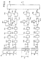
- FIG. 5 represents a first application of the device according to the invention for which the reading register comprises two outputs.
- the reading register is split in a manner known per se into a so-called “even” register and a so-called register “odd”.
- the even register collects the charges accumulated in the pixels of even rank of the photosensitive zone and the odd register recovers the charges accumulated in the odd rank pixels of the area photosensitive.
- a DI device rearranges Sla and Slb signals from respective sort operators TRa and TRb.
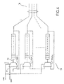
- Figure 6 shows a second application of the device according to the invention for which the read register comprises a number Q of outputs.
- the reading register RL consists of Q sub-registers (R1, R2, ..., Rj, ..., RQ) and each sub-register includes M transfer stages.
- M has been chosen, by way of example, equal to 6.
- the device according to the invention however relates to other modes where M is any integer that can be different for two different sub-registers.
- the M transfer stages of each sub-register Rj follow one another so that the transfer of charges is carried out from the stage of row 1 towards the stage of row M.
- the reading diode of the load-voltage converter of the sub-register Rj of rank j is integrated in the transfer stage of rank M of the sub-register Ri. This floor of transfer is denoted ESj in FIG. 6 and will subsequently be called the stage of intermediate outlet.
- the charge-voltage converter of each sub-register Rj is generally made up of the read diode contained in the output stage intermediate ESj and a first reading amplifier Aj which may or may not, in whole or in part, be integrated into the component to which the registry belongs reading.
- an MOS transistor preloads the capacity of the diode before the arrival of the charge conveyed in the sub-register Rj.
- the signals SI1 SI2, ..., SIj, ..., SIQ from the respective sorting operators TR1, TR2, ..., TRj, ..., TRQ are rearranged in a DI device.
- FIG. 7 represents the view according to section A-A of FIG. 6.
- a fraction of the sub-register Rj is represented. of rank j as well as a fraction of the sub-register Rj + 1 of rank j + 1.
- the represented fraction of the sub-register Rj consists of a stage of ET transfer of known type and the intermediate output stage ESj.
- the represented fraction of the sub-register Rj + 1 is a fraction of the stage of ET transfer of known type which adjoins the intermediate output stage ESj.
- the transfer mode chosen is of the two-phase type.
- the invention however relates to transfer modes the number of which phases is greater than two.
- the ET transfer stage is formed in a P-doped substrate 1.
- An N-doped layer 2 covers the substrate 1 so as to constitute a buried channel.
- the layer 2 doped N consists of a succession of alternately doped regions N - doped region and N.
- N - means a doped zone N but in less proportion than an N-doped zone.
- An electrically insulating layer 3 covers the doped layer 2. The electrodes which allow the transfer are produced above the electrically insulating layer 3.
- four electrodes E1, E2, E3, E4 participate in the transfer of charges in the stage AND.
- the 4 successive electrodes E1, E2, E3, E4 respectively cover doped zones N - , N, N - , N of the buried channel 2
- the two electrodes E1 and E2 are connected to the same phase Phi1 and the two electrodes E3 and E4 are connected to the same phase Phi2.
- the phases Phi1 and Phi2 are adjusted in a known manner in order to ensure the transfer of charges from the transfer stage AND from the sub-register Rj to the intermediate output stage ESj of the same sub-register.
- the intermediate output stage ESj is also formed in the P-doped substrate 1.
- the intermediate output stage successively comprises: two electrodes E6 and E7 connected to the same phase Phi1, an output electrode 4 to which a voltage Vg is applied, an N + doped area 5 and a P + doped area 6, the areas 5 and 6 are both formed in the substrate 1.
- the reading diode is formed by the junction between the N + doped zone and the P doped substrate 1.
- the electrodes E6 and E7 are located on the surface of the electrically insulating layer 3 and respectively cover an N-doped area - and an N-doped area of the buried channel 2.
- the electrode 4 is also located on the surface of the layer 3 and covers a N - doped area.
- the voltage Vg applied to the electrode 4 allows the transfer of the charges in the reading diode.
- Zone 6 doped P + constitutes an isolation barrier between the sub-register Rj and the sub-register Rj + 1.
- the voltage which appears at the terminals of the read diode is applied to the input of the first read amplifier Aj (not shown in the figure) via the conductive connection Kj.
- the intermediate output stage collects the charges accumulated in the pixel which adjoins it.
- the transfer of charges to the output amplifier Aj of each sub-register Ri then takes place without dead time.
- the N + doped zone 5 stretches in the direction perpendicular to the direction of propagation of the charges over the entire width of the intermediate output stage. It follows that the electric field which makes it possible to accelerate the charges towards the diode is constant. The acceleration of the charges being uniform, their transfer also takes place uniformly and, therefore, faster than in the read registers of known type.
- Figure 8 shows the sectional view A-A of Figure 6 of a second embodiment of the reading register.
- figure 8 represents a fraction of the sub-register Rj of rank j as well as a fraction of the sub-register Rj + 1 of rank j + 1.
- the transfer mode chosen is of the two-phase type, but, as has been mentioned previously, the invention also relates to modes of transfer whose number of phases is greater than two.
- the ET transfer stages represented in FIG. 8 are identical to those represented in FIG. 7. The same is true of the intermediate output stage ESj except with regard to the element making it possible to constitute the insulation barrier between the sub -register Rj and the sub-register Rj + 1.
- the insulation barrier is produced by an electrode 7 to which a potential Vi is applied.
- the electrode 7 is located on the surface of the layer 3 and covers an N - doped area.
- the use of a photosensitive device such that that described in FIG. 6 makes it possible to provide very information rates high.
- the use of an TL6 optoelectronic detector having 1024 pixels and 32 outputs and used for reading a strip of 1,000 tracks provides an information flow of the order of several hundred Mbits per second.
Landscapes
- Engineering & Computer Science (AREA)
- Multimedia (AREA)
- Signal Processing (AREA)
- Signal Processing For Digital Recording And Reproducing (AREA)
- Complex Calculations (AREA)
- Optical Recording Or Reproduction (AREA)
Claims (15)
- Verfahren zum Lesen binärer Informationen, die in einen Träger geschrieben sind und sich in verschiedenen Spuren (p1, ..., pX) befinden, wobei die binären Informationen in den Träger mit der Frequenz Fbit geschrieben worden sind, dadurch gekennzeichnet, daß es umfaßt:wobei die Koeffizienten ak-i, ..., ak, ..., ak+j Werte besitzen, die vom gewählten Interpolationsgesetz abhängen, undeinen Schritt, in dem die binären Informationen mit der Abtastfrequenz Fe, die größer als die Frequenz Fbit ist, gelesen werden und gleichzeitig die binären Informationen derselben Ordnung k in den verschiedenen Spuren gelesen werden, derart, daß eine Folge aufeinanderfolgender gelesener Abtastwerte ECH(k) für jede Spur gebildet wird, wobei ECH(k) der gelesene Abtastwert der Ordnung k ist, wobei jeder gelesene Abtastwert der Ordnung k eine Phase ϕ(k) im Bereich von 0 bis 2π besitzt,einen Interpolationsschritt, der es ermöglicht, einen interpolierten Abtastwert I(k) mit Phase π, der dem gelesenen Abtastwert ECH(k) entspricht, anhand des gelesenen Abtastwerts ECH(k) und der i + j gelesenen Abtastwerte (ECH(k - i), ..., ECH(k + j)) in derselben Spur, die den gelesenen Abtastwert ECH(k) umgeben, zu berechnen, derart, daß:
einen Validierungsschritt, der es ermöglicht, eine Information (VAL) zu erzeugen, die dazu bestimmt ist, den interpolierten Abtastwert I(k) für gültig oder ungültig zu erklären,
wobei der Interpolationsschritt Verzögerungsphasen enthält, derart, daß die verarbeiteten aufeinanderfolgenden Abtastwerte aufeinanderfolgende Informationen derselben Spur repräsentieren. - Leseverfahren nach Anspruch 1, dadurch gekennzeichnet, daß der Validierungsschritt darin besteht, die Größe π + π mit dem Intervall [ϕ(k), ϕ(k + 1)[ zu vergleichen, derart, daß es die Information (VAL) ermöglicht, den interpolierten Abtastwert I(k) für gültig zu erklären, falls π + π in diesem Intervall enthalten ist, oder den interpolierten Abtastwert I(k) für nicht gültig zu erklären, falls π + π nicht in diesem Intervall enthalten ist.
- Leseverfahren nach einem der Ansprüche 1 oder 2, dadurch gekennzeichnet, daß die Werte der Koeffizienten ak-i, ..., ak, ak+j in Tabellen enthalten sind und in Abhängigkeit vom Wert der Phase ϕ(k) des Abtastwerts ECH(k) ausgewählt werden.
- Leseverfahren nach Anspruch 3, dadurch gekennzeichnet, daß die Werte der Koeffizienten für N Phasensegmente, die das Intervall [0, 2π] unterteilen, im voraus berechnet werden und daß die für die Koeffizienten gewählten Werte jene sind, die dem Phasenintervall entsprechen, zu dem die Phase ϕ(k) des Abtastwerts ECH(k) gehört.
- Leseverfahren nach einem der Ansprüche 1 oder 2, dadurch gekennzeichnet, daß die Werte, die die Größen ak-iECH(k - i), ..., akECH(k), ..., ak+jECH(k + j) annehmen können, für N Phasensegmente, die das Intervall [0, 2π] unterteilen, im voraus berechnet werden, wobei die Werte der Abtastwerte ECH(k - i), ..., ECH(k), ..., ECH(k + j) aus allen Werten genommen werden, die die Abtastwerte annehmen können, und daß die für die Größen gewählten Werte jene sind, die dem Abtastwert ECH(k) und dem Phasenintervall, zu dem die Phase ϕ(k) des Abtastwertes ECH(k) gehört, entsprechen.
- Leseverfahren nach einem der vorhergehenden Ansprüche, dadurch gekennzeichnet, daß es einen Schritt umfaßt, in dem die interpolierten Abtastwerte je nachdem, ob die interpolierten Abtastwerte für gültig oder nicht gültig erklärt werden müssen, sortiert werden.
- Leseverfahren nach Anspruch 6, dadurch gekennzeichnet, daß der Sortierungsschritt ermöglicht, die für gültig erklärten interpolierten Abtastwerte in Paketen anzuordnen, derart, daß eine Folge von Wörtern gebildet wird.
- Leseverfahren nach Anspruch 6, dadurch gekennzeichnet, daß es das Lesen einer einzigen Spur betrifft und daß der Sortierungsschritt darin besteht, die interpolierten Abtastwerte im Takt der Information (VAL), die dazu bestimmt ist, die interpolierten Abtastwerte für gültig zu erklären, zu speichern.
- System zum Lesen binärer Informationen, die in einen magnetischen Träger geschrieben sind und sich in verschiedenen Spuren (p1, ..., pX) befinden, wobei die binären Informationen in den Träger mit der Frequenz Fbit geschrieben worden sind, mit:wobei die Koeffizienten ak-i, ..., ak, ..., ak+j Werte besitzen, die vom gewählten Interpolationsgesetz abhängen, undLesemitteln, die es ermöglichen, die binären Informationen mit einer Abtastfrequenz Fe, die größer als die Frequenz Fbit ist, zu lesen und gleichzeitig die binären Informationen desselben Rangs k in den verschiedenen Spuren zu lesen, derart, daß eine Folge aufeinanderfolgender gelesener Abtastwerte ECH(k) für jede Spur erhalten wird, wobei k der Rang des Abtastwerts ECH(k) in jeder Spur ist, wobei jeder gelesene Abtastwert mit Rang k eine Phase ϕ(k) im Bereich von 0 bis 2π besitzt;Interpolationsmitteln, die es ermöglichen, einen interpolierten Abtastwert I(k) mit Phase π für jeden gelesenen Abtastwert ECH(k) anhand des Abtastwerts ECH(k) und der i + j gelesenen Abtastwerte, die den Abtastwert ECH(k) in derselben Spur umgeben, zu berechnen, derart, daß:wobei die Interpolationsmittel Verzögerungsmittel vorsehen, derart, daß die verarbeiteten aufeinanderfolgenden Abtastwerte aufeinanderfolgende Informationen derselben Spur repräsentieren.Validierungsmitteln, die es ermöglichen, eine Information (VAL) zu erzeugen, die dazu bestimmt ist, den interpolierten Abtastwert I(k) für gültig oder für nicht gültig zu erklären,
- System zum Lesen von Informationen nach Anspruch 9, dadurch gekennzeichnet, daß es umfaßt:wobei die Koeffizienten ak-i, ..., ak, ..., ak+j Werte besitzen, die vom gewählten Interpolationsgesetz abhängen, und wobei die Validierungsmittel es ermöglichen, eine Information (VAL) zu erzeugen, die dazu bestimmt ist, den interpolierten Abtastwert I(k) für gültig oder nicht gültig zu erklären.einen magnetooptischen Lesekopf, der ermöglicht, die gleichzeitig in wenigstens einer Spur mit der Abtastfrequenz Fe gelesenen binären Informationen in Lichtinformationen umzuwandeln,eine lichtempfindliche Vorrichtung mit Ladungsübertragung, die die Lichtinformationen sammelt und es ermöglicht, die Lichtinformationen in eine Folge von Spannungsabtastwerten umzuwandeln, wobei die lichtempfindliche Vorrichtung wenigstens einen Ausgang aufweist, an dem die Spannungsabtastwerte ausgegeben werden, undVerzögerungsmittel (1, 2), die mit dem Ausgang verbunden sind und es ermöglichen, die am Ausgang gesammelten Spannungsabtastwerte umzuordnen, derart, daß eine Folge aufeinanderfolgender gelesener Abtastwerte ECH(k) derselben Spur erhalten wird, wobei k der Rang des Abtastwerts ECH(k) in der Spur ist, wobei die Interpolationsmittel es ermöglichen, einen interpolierten Abtastwert I(k) für jeden gelesenen Abtastwert ECH(k) anhand des Abtastwerts ECH(k) und der i + j gelesenen Abtastwerte, die den Abtastwert ECH(k) umgeben, zu berechnen, derart, daß
- System zum Lesen binärer Informationen nach einem der Ansprüche 9 oder 10, dadurch gekennzeichnet, daß die Interpolationsmittel aus i + j + 1 Multiplizierern (7, 8, 9), wovon jeder einen ersten Eingang und einen zweiten Eingang besitzt, und aus einem Summierer (10) gebildet sind, wobei die i + j + 1 aufeinanderfolgenden Abtastwerte ECH(k - i), ..., ECH(k), ..., ECH(k + j) in den ersten Eingang eines entsprechenden der i + j + 1 Multiplizierer (7, 8, 9) eingegeben werden, während die zweiten Eingänge der Multiplizierer die entsprechenden Koeffizienten ak-i, ..., ak, ..., ak+j empfangen, wobei das von jedem Multiplizierer ausgegebene Ergebnis in den Summierer (10) geschickt wird, derart, daß der interpolierte Abtastwert I(k) erhalten wird, und daß die Validierungsmittel aus einem Validierungsoperator (6) gebildet sind, an den die Phase ϕ(k) des gelesenen Abtastwerts ECH(k) und die Phase ϕ(k + 1) des gelesenen Abtastwerts ECH(k + 1) geschickt werden, derart, daß der Validierungsoperator dann, wenn die Größe π + π zu dem Intervall [ϕ(k), ϕ(k + 1)[ gehört, ein Signal (VAL) erzeugt, das es ermöglicht, den interpolierten Abtastwert für gültig zu erklären, und daß der Validierungsoperator dann, wenn die Größe π + π nicht zu diesem Intervall gehört, ein Signal erzeugt, das es ermöglicht, den interpolierten Abtastwert für nicht gültig zu erklären.
- Lesesystem nach einem der Ansprüche 9, 10 oder 11, dadurch gekennzeichnet, daß es einen Sortierungsoperator (TRI) umfaßt, der ermöglicht, nur die für gültig erklärten interpolierten Abtastwerte beizubehalten.
- Lesesystem nach einem der Ansprüche 10 bis 12, dadurch gekennzeichnet, daß die lichtempfindliche Vorrichtung mit Ladungsübertragung aus einer lichtempfindlichen Zone, die aus einer geradlinigen Anordnung von Bildelementen gebildet ist, und aus einer nicht lichtempfindlichen Zone gebildet ist, welche aus einem aus Übertragungsstufen gebildeten Leseregister (RL) gebildet ist, wobei die in einem Bildelement erzeugten Ladungen in einer Übertragungsstufe des Leseregisters gesammelt werden, das Leseregister (RL) aus Q Unterregistern (R1, R2, ..., Rj, ..., RQ) gebildet ist, jedes Unterregister Rj M Übertragungsstufen umfaßt, wobei M eine beliebige ganze Zahl ist, die für zwei verschiedene Unterregister verschieden sein kann, die M Übertragungsstufen jedes Unterregisters in der Weise aufeinander folgen, daß die Übertragung von Ladungen von der Stufe mit Rang 1 zur Stufe mit Rang M erfolgt, die Übertragungsstufe mit Rang M jedes Unterregisters eine Lesediode enthält, die es ermöglicht, die Ladungsveränderungen, die sie erfaßt, in Spannungsänderungen umzuwandeln, und jede Lesediode jedes Unterregisters einen Ausgang des Leseregisters (RL) bildet.
- Lesesystem nach einem der Ansprüche 9 oder 10, dadurch gekennzeichnet, daß der magnetische Träger mehrere Informationsspuren umfaßt, die asynchron lesbar sind.
- Leseverfahren nach Anspruch 1, dadurch gekennzeichnet, daß der magnetische Träger mehrere Informationsspuren umfaßt, die asynchron lesbar sind.
Applications Claiming Priority (3)
| Application Number | Priority Date | Filing Date | Title |
|---|---|---|---|
| FR9504820A FR2733346B1 (fr) | 1995-04-21 | 1995-04-21 | Procede de lecture d'informations |
| FR9504820 | 1995-04-21 | ||
| PCT/FR1996/000601 WO1996033490A1 (fr) | 1995-04-21 | 1996-04-19 | Procede de lecture d'informations |
Publications (2)
| Publication Number | Publication Date |
|---|---|
| EP0766863A1 EP0766863A1 (de) | 1997-04-09 |
| EP0766863B1 true EP0766863B1 (de) | 2002-09-25 |
Family
ID=9478352
Family Applications (1)
| Application Number | Title | Priority Date | Filing Date |
|---|---|---|---|
| EP96915061A Expired - Lifetime EP0766863B1 (de) | 1995-04-21 | 1996-04-19 | Verfahren zum lesen von informationen |
Country Status (8)
| Country | Link |
|---|---|
| US (1) | US5963525A (de) |
| EP (1) | EP0766863B1 (de) |
| JP (1) | JPH10505936A (de) |
| CN (1) | CN1114915C (de) |
| DE (1) | DE69623898T2 (de) |
| DK (1) | DK0766863T3 (de) |
| FR (1) | FR2733346B1 (de) |
| WO (1) | WO1996033490A1 (de) |
Families Citing this family (7)
| Publication number | Priority date | Publication date | Assignee | Title |
|---|---|---|---|---|
| EP1196914B1 (de) | 1999-07-09 | 2003-04-09 | Thales | Spurfolgesystem zur aufzeichnung/wiedergabe eines informationsträgers und aufzeichnungsträger |
| FR2797514B3 (fr) * | 1999-08-10 | 2001-10-12 | Thomson Csf | Dispositif de lecture magneto-optique pour bandes magnetiques multipistes |
| US6418101B1 (en) * | 1999-09-03 | 2002-07-09 | Zen Research (Ireland), Ltd. | Digital read channel for optical disk reader |
| JP3486145B2 (ja) * | 2000-01-17 | 2004-01-13 | 松下電器産業株式会社 | デジタル記録データ再生装置 |
| US6693872B1 (en) * | 2000-08-29 | 2004-02-17 | Eastman Kodak Company | Multi-track optical data recording and readout |
| DE10141597B4 (de) * | 2001-08-24 | 2017-11-09 | Lantiq Deutschland Gmbh | Verfahren zum Rekonstruieren von über eine Übertragungsstrecke übertragenen Daten in einem Empfänger und entsprechende Vorrichtung |
| JP2004079015A (ja) * | 2002-08-09 | 2004-03-11 | Fujitsu Ltd | データ再生装置 |
Family Cites Families (14)
| Publication number | Priority date | Publication date | Assignee | Title |
|---|---|---|---|---|
| US4707841A (en) * | 1984-08-21 | 1987-11-17 | University Of Toronto, Innovations Foundation | Digital data receiver for preamble free data transmission |
| US4780892A (en) * | 1984-10-05 | 1988-10-25 | Willi Studer Ag | Scanning frequency synchronization method and apparatus |
| NL8600931A (nl) * | 1986-04-14 | 1987-11-02 | Philips Nv | Werkwijze en inrichting voor het restaureren van ongeldige monsters van een equidistant bemonsterd signaal. |
| US4815067A (en) * | 1986-10-06 | 1989-03-21 | Thorn Emi Plc. | Optical rotary headwheel tape recording system |
| GB2224911A (en) * | 1988-11-09 | 1990-05-16 | Philips Nv | Method of and apparatus for assigning binary values to sample values |
| EP0548359B1 (de) * | 1989-10-23 | 1996-04-24 | Matsushita Electric Industrial Co., Ltd. | Digitales signalwiedergabegerät mit variabler geschwindigkeit |
| JP3194752B2 (ja) * | 1991-01-31 | 2001-08-06 | パイオニア株式会社 | Pcmディジタルオーディオ信号再生装置 |
| JPH0562495A (ja) * | 1991-09-02 | 1993-03-12 | Pioneer Electron Corp | サンプリング周波数変換器 |
| US5586100A (en) * | 1992-10-13 | 1996-12-17 | Literal Corporation | Transversal filter and method for cancelling intersymbol interference |
| FR2699724B1 (fr) * | 1992-12-22 | 1995-01-20 | Thomson Csf | Procédé de lecture d'un support d'enregistrement et système appliquant ce procédé. |
| BE1007872A3 (nl) * | 1993-12-15 | 1995-11-07 | Philips Electronics Nv | Optische aftastinrichting, alsmede een opteken- en/of uitleesinrichting voorzien van een dergelijke aftastinrichting. |
| JPH07220409A (ja) * | 1994-02-04 | 1995-08-18 | Pioneer Electron Corp | ディジタル信号再生装置 |
| JP2922113B2 (ja) * | 1994-04-06 | 1999-07-19 | 松下電送システム株式会社 | 画像記録装置 |
| US5602811A (en) * | 1994-08-11 | 1997-02-11 | Yamaha Corporation | Musical information recording and reproducing technique for use with a recording medium having a UTOC area |
-
1995
- 1995-04-21 FR FR9504820A patent/FR2733346B1/fr not_active Expired - Fee Related
-
1996
- 1996-04-19 JP JP8530789A patent/JPH10505936A/ja active Pending
- 1996-04-19 US US08/750,798 patent/US5963525A/en not_active Expired - Lifetime
- 1996-04-19 DK DK96915061T patent/DK0766863T3/da active
- 1996-04-19 EP EP96915061A patent/EP0766863B1/de not_active Expired - Lifetime
- 1996-04-19 DE DE69623898T patent/DE69623898T2/de not_active Expired - Lifetime
- 1996-04-19 WO PCT/FR1996/000601 patent/WO1996033490A1/fr not_active Ceased
- 1996-04-19 CN CN96190371A patent/CN1114915C/zh not_active Expired - Fee Related
Also Published As
| Publication number | Publication date |
|---|---|
| DE69623898D1 (de) | 2002-10-31 |
| US5963525A (en) | 1999-10-05 |
| DK0766863T3 (da) | 2003-01-27 |
| CN1114915C (zh) | 2003-07-16 |
| CN1150857A (zh) | 1997-05-28 |
| EP0766863A1 (de) | 1997-04-09 |
| WO1996033490A1 (fr) | 1996-10-24 |
| FR2733346B1 (fr) | 1997-05-23 |
| DE69623898T2 (de) | 2003-05-15 |
| JPH10505936A (ja) | 1998-06-09 |
| FR2733346A1 (fr) | 1996-10-25 |
Similar Documents
| Publication | Publication Date | Title |
|---|---|---|
| FR2471109A1 (fr) | Magnetoscope numerique | |
| EP0627114B1 (de) | Verfahren zum lezen eines aufzeichnungstragers und system das dieses verfahren anwendet | |
| FR2475828A1 (fr) | Procede et appareil permettant d'extraire d'un signal numerique une information temporelle | |
| FR2611299A1 (fr) | Systeme d'enregistrement d'albums sur mesure | |
| EP0125722A1 (de) | Schaltungsanordnung zur kombinierten adaptativen Entzerrung und Demodulation | |
| EP0766863B1 (de) | Verfahren zum lesen von informationen | |
| EP0501857A1 (de) | Seismischertransmissionsverfahren und -gerät mit niedriger Fehlerrate | |
| EP0627113B1 (de) | Datenaufzeichnungstrager,aufzeichnungs,wiedegabegerat und verfahren zur aufzeichnung | |
| EP0549412B1 (de) | Zeittaktschaltung für Lesegerät für sequentielle Daten | |
| EP0714091B1 (de) | Lesevorrichtung und -system | |
| EP0434547B1 (de) | Mehrspur-Lesemagnetkopf | |
| EP0295979B1 (de) | Verfahren zur Aufzeichnung von Information auf einem magnetischen Aufzeichnungsträger | |
| EP0094852A1 (de) | Opto-elektronisches Verfahren zum Lesen von Informationen von einer magnetischen Platte und Anordnung dafür | |
| EP0718826B1 (de) | Lesevorrichtung und -system | |
| FR2613560A1 (fr) | Egaliseur automatique pour transmission numerique | |
| EP0677844B1 (de) | Lesesystem für einen Mehrspur-Aufzeichnungsträger | |
| FR2511171A1 (fr) | Appareil et procede pour determiner la position d'une tete de lecture | |
| EP1511200A1 (de) | Vorrichtung zur Regenerierung eines optischen Signals und entsprechendes Verfahren | |
| NO318778B1 (no) | Fremgangsmate og anordning ved lesing av informasjon pa en baerer, spesielt binaer informasjon | |
| EP0295164A1 (de) | Verfahren zum Schreiben von Synchronisierungsinformation auf einen magnetischen Augzeichnungsträger | |
| KR100553107B1 (ko) | 2진정보판독시스템및방법 | |
| WO2001004879A1 (fr) | Systeme de suivi de piste pour l'enregistrement/lecture d'un support d'informations et support d'enregistrement | |
| FR2464531A1 (fr) | Appareil et procede de reproduction d'information numerique enregistree sur un support magnetique | |
| FR2705850A1 (fr) | Dispositif de rephasage d'un signal numérique transmis suivant une transmission synchrone et susceptible d'être affecté de gigue. | |
| EP0031774A2 (de) | -16-stufiges MAMSK-Modulationsverfahren für digitales Datenübertragungssystem sowie Modulatoren und Demodulator dafür |
Legal Events
| Date | Code | Title | Description |
|---|---|---|---|
| PUAI | Public reference made under article 153(3) epc to a published international application that has entered the european phase |
Free format text: ORIGINAL CODE: 0009012 |
|
| 17P | Request for examination filed |
Effective date: 19960916 |
|
| AK | Designated contracting states |
Kind code of ref document: A1 Designated state(s): DE DK FR GB IT NL SE Kind code of ref document: A1 Designated state(s): DE ES FR GB IT NL SE |
|
| RAP1 | Party data changed (applicant data changed or rights of an application transferred) |
Owner name: THOMSON MULTIMEDIA Owner name: THOMSON-CSF |
|
| 17Q | First examination report despatched |
Effective date: 19991217 |
|
| RAP1 | Party data changed (applicant data changed or rights of an application transferred) |
Owner name: THOMSON MULTIMEDIA Owner name: THALES |
|
| GRAG | Despatch of communication of intention to grant |
Free format text: ORIGINAL CODE: EPIDOS AGRA |
|
| GRAG | Despatch of communication of intention to grant |
Free format text: ORIGINAL CODE: EPIDOS AGRA |
|
| GRAH | Despatch of communication of intention to grant a patent |
Free format text: ORIGINAL CODE: EPIDOS IGRA |
|
| GRAH | Despatch of communication of intention to grant a patent |
Free format text: ORIGINAL CODE: EPIDOS IGRA |
|
| GRAA | (expected) grant |
Free format text: ORIGINAL CODE: 0009210 |
|
| RBV | Designated contracting states (corrected) |
Designated state(s): DE DK FR GB IT NL SE |
|
| AK | Designated contracting states |
Kind code of ref document: B1 Designated state(s): DE DK FR GB IT NL SE |
|
| REG | Reference to a national code |
Ref country code: GB Ref legal event code: FG4D Free format text: NOT ENGLISH |
|
| REF | Corresponds to: |
Ref document number: 69623898 Country of ref document: DE Date of ref document: 20021031 |
|
| GBT | Gb: translation of ep patent filed (gb section 77(6)(a)/1977) |
Effective date: 20021130 |
|
| REG | Reference to a national code |
Ref country code: DK Ref legal event code: T3 |
|
| PLBE | No opposition filed within time limit |
Free format text: ORIGINAL CODE: 0009261 |
|
| STAA | Information on the status of an ep patent application or granted ep patent |
Free format text: STATUS: NO OPPOSITION FILED WITHIN TIME LIMIT |
|
| 26N | No opposition filed |
Effective date: 20030626 |
|
| PGFP | Annual fee paid to national office [announced via postgrant information from national office to epo] |
Ref country code: GB Payment date: 20130424 Year of fee payment: 18 Ref country code: DE Payment date: 20130419 Year of fee payment: 18 Ref country code: DK Payment date: 20130410 Year of fee payment: 18 Ref country code: SE Payment date: 20130412 Year of fee payment: 18 |
|
| PGFP | Annual fee paid to national office [announced via postgrant information from national office to epo] |
Ref country code: NL Payment date: 20130410 Year of fee payment: 18 Ref country code: FR Payment date: 20130521 Year of fee payment: 18 Ref country code: IT Payment date: 20130422 Year of fee payment: 18 |
|
| REG | Reference to a national code |
Ref country code: DE Ref legal event code: R119 Ref document number: 69623898 Country of ref document: DE |
|
| REG | Reference to a national code |
Ref country code: DK Ref legal event code: EBP Effective date: 20140430 |
|
| REG | Reference to a national code |
Ref country code: NL Ref legal event code: V1 Effective date: 20141101 |
|
| REG | Reference to a national code |
Ref country code: SE Ref legal event code: EUG |
|
| GBPC | Gb: european patent ceased through non-payment of renewal fee |
Effective date: 20140419 |
|
| REG | Reference to a national code |
Ref country code: DE Ref legal event code: R119 Ref document number: 69623898 Country of ref document: DE Effective date: 20141101 |
|
| REG | Reference to a national code |
Ref country code: FR Ref legal event code: ST Effective date: 20141231 |
|
| PG25 | Lapsed in a contracting state [announced via postgrant information from national office to epo] |
Ref country code: DE Free format text: LAPSE BECAUSE OF NON-PAYMENT OF DUE FEES Effective date: 20141101 Ref country code: GB Free format text: LAPSE BECAUSE OF NON-PAYMENT OF DUE FEES Effective date: 20140419 Ref country code: SE Free format text: LAPSE BECAUSE OF NON-PAYMENT OF DUE FEES Effective date: 20140420 |
|
| PG25 | Lapsed in a contracting state [announced via postgrant information from national office to epo] |
Ref country code: FR Free format text: LAPSE BECAUSE OF NON-PAYMENT OF DUE FEES Effective date: 20140430 Ref country code: NL Free format text: LAPSE BECAUSE OF NON-PAYMENT OF DUE FEES Effective date: 20141101 |
|
| PG25 | Lapsed in a contracting state [announced via postgrant information from national office to epo] |
Ref country code: IT Free format text: LAPSE BECAUSE OF NON-PAYMENT OF DUE FEES Effective date: 20140419 |
|
| PG25 | Lapsed in a contracting state [announced via postgrant information from national office to epo] |
Ref country code: DK Free format text: LAPSE BECAUSE OF NON-PAYMENT OF DUE FEES Effective date: 20140430 |