EP0772246A1 - Kondensator mit hoher Kapazität und dessen Herstellungsverfahren - Google Patents
Kondensator mit hoher Kapazität und dessen Herstellungsverfahren Download PDFInfo
- Publication number
- EP0772246A1 EP0772246A1 EP95830459A EP95830459A EP0772246A1 EP 0772246 A1 EP0772246 A1 EP 0772246A1 EP 95830459 A EP95830459 A EP 95830459A EP 95830459 A EP95830459 A EP 95830459A EP 0772246 A1 EP0772246 A1 EP 0772246A1
- Authority
- EP
- European Patent Office
- Prior art keywords
- layer
- capacitor
- polycrystalline silicon
- poly2
- type
- Prior art date
- Legal status (The legal status is an assumption and is not a legal conclusion. Google has not performed a legal analysis and makes no representation as to the accuracy of the status listed.)
- Granted
Links
- 239000003990 capacitor Substances 0.000 title claims abstract description 89
- 238000004519 manufacturing process Methods 0.000 title description 2
- 229910021420 polycrystalline silicon Inorganic materials 0.000 claims abstract description 34
- 239000002019 doping agent Substances 0.000 claims abstract description 19
- 238000009792 diffusion process Methods 0.000 claims abstract description 18
- 239000004065 semiconductor Substances 0.000 claims abstract description 13
- 239000000758 substrate Substances 0.000 claims abstract description 10
- 238000002955 isolation Methods 0.000 claims abstract description 6
- 238000000034 method Methods 0.000 claims description 12
- 230000008569 process Effects 0.000 claims description 10
- 238000003860 storage Methods 0.000 claims description 6
- 238000000151 deposition Methods 0.000 claims description 5
- 238000001465 metallisation Methods 0.000 claims description 5
- 238000012546 transfer Methods 0.000 claims description 5
- 230000006870 function Effects 0.000 description 4
- 230000015654 memory Effects 0.000 description 3
- 238000013459 approach Methods 0.000 description 2
- 230000008901 benefit Effects 0.000 description 2
- 238000010276 construction Methods 0.000 description 2
- 238000010586 diagram Methods 0.000 description 2
- 230000010354 integration Effects 0.000 description 2
- 229910045601 alloy Inorganic materials 0.000 description 1
- 239000000956 alloy Substances 0.000 description 1
- 230000004888 barrier function Effects 0.000 description 1
- 230000015572 biosynthetic process Effects 0.000 description 1
- 230000008859 change Effects 0.000 description 1
- 230000008021 deposition Effects 0.000 description 1
- 229910052751 metal Inorganic materials 0.000 description 1
- 239000002184 metal Substances 0.000 description 1
- 150000002739 metals Chemical class 0.000 description 1
- 230000004048 modification Effects 0.000 description 1
- 238000012986 modification Methods 0.000 description 1
- 229920005591 polysilicon Polymers 0.000 description 1
- 229910052710 silicon Inorganic materials 0.000 description 1
- 210000000352 storage cell Anatomy 0.000 description 1
- 238000012360 testing method Methods 0.000 description 1
Images


Classifications
-
- H—ELECTRICITY
- H10—SEMICONDUCTOR DEVICES; ELECTRIC SOLID-STATE DEVICES NOT OTHERWISE PROVIDED FOR
- H10D—INORGANIC ELECTRIC SEMICONDUCTOR DEVICES
- H10D1/00—Resistors, capacitors or inductors
- H10D1/60—Capacitors
- H10D1/68—Capacitors having no potential barriers
-
- H—ELECTRICITY
- H10—SEMICONDUCTOR DEVICES; ELECTRIC SOLID-STATE DEVICES NOT OTHERWISE PROVIDED FOR
- H10D—INORGANIC ELECTRIC SEMICONDUCTOR DEVICES
- H10D1/00—Resistors, capacitors or inductors
- H10D1/60—Capacitors
- H10D1/62—Capacitors having potential barriers
- H10D1/66—Conductor-insulator-semiconductor capacitors, e.g. MOS capacitors
Definitions
- This invention relates to a high-capacitance capacitor.
- the invention relates to a high-capacitance capacitor which can be monolithically integrated on a semiconductor substrate doped with a first type of dopant, the substrate containing a diffusion well doped with a second type of dopant and formed with a first active region therein, and a gate oxide layer being deposited onto said diffusion well which is covered with a first layer of polycrystalline silicon and separated from a second layer of polycrystalline silicon by an interpoly dielectric layer.
- the invention also concerns a process for integrating a high-capacitance capacitor on a semiconductor substrate doped with a first type of dopant, which process comprises the steps of defining a well doped with a second type of dopant, implanting and then diffusing a first diffused region doped to a higher concentration of dopant of the second type, depositing a gate oxide layer over the diffusion well, covering said oxide layer with a first layer of polycrystalline silicon, and depositing a second dielectric layer referred to as the interpoly oxide.
- the invention relates, specifically but not exclusively, to a high-capacitance capacitor adapted to be integrated to a current step-up circuit for non-volatile semiconductor memories, and the description which follows will make specific reference to this field of application for convenience of illustration.
- Voltage step-up or "booster" circuits have been employed for the purpose which can provide such higher voltages, even internally of the integrated circuit.
- electrically programmable non-volatile memories e.g. of the Flash EEPROM type, require a write voltage far above the conventional 5-volt supply.
- Vp programming voltage
- boost voltage-multiplying circuit
- a voltage-multiplying circuit is known, for example, from European Patent Application No. EP-A-0 540 948, published on May 12, 1993.
- the voltage multiplier described in that patent application is of a type known as "charge pump” and requires at least two capacitors.
- a first capacitor functions to draw and transfer electric charges, from the input terminal of the multiplier to the output terminal, and the second capacitor functions to store up the charges.
- capacitors could be used, connected in series or parallel configurations to provide an equivalent capacitor of greater overall capacitance.
- the underlying technical problem of this invention is to provide a high-capacitance capacitor whereby the ratio of electric charge storage capacity to occupied area can be optimized, overcoming the drawbacks with which prior solutions are beset.
- the solution idea on which this invention stands is to provide a high-capacitance capacitor by utilizing the interpoly oxide in a structure integrated on a semiconductor with a process of the MOS type.
- a capacitor which comprises first and second elementary capacitors formed from two layers of polycrystalline silicon deposited onto an active area of the integrated circuit and separated by an interpoly dielectric layer.
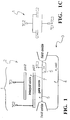
- a high-capacitance capacitor according to the invention as formed on an integrated structure 2 basically of a sandwich type.
- the structure 2 comprises a semiconductor substrate 3 doped with a first dopant, e.g. of the P type, wherein a diffusion well 4 has been formed which is doped with a second dopant of the N type.
- a first dopant e.g. of the P type
- a diffusion well 4 has been formed which is doped with a second dopant of the N type.
- a first diffused region 5 which has a higher concentration of the second dopant type N+.
- a diffused region 5 doped P+ could be provided instead.
- a diffused region 5 of either the N+ or P+ type may be formed.
- Shown in Figure 1A is a modified embodiment of the integrated structure 2 on which the high-capacitance capacitor 1 of this invention is formed.
- the second layer POLY2 consists of first POLY2A and second POLY2B layer portions which are structurally independent and isolated from each other.
- the first portion POLY2A has a first contact terminal TC1.
- the second portion POLY2B is in direct contact with the first layer POLY1 of polycrystalline silicon and includes a second contact terminal TC2.
- the second polysilicon layer will be subjected to the metallization which leads to the formation of the contact terminals for the capacitor 1.
- the second contact terminal TC2 is, therefore, separated from the first contact terminal TC1.
- the first layer P1 of polycrystalline silicon does not contact the second layer P2, and has the first contact terminal TC1 only.
- the contact metallization is carried out directly on the first layer of polycrystalline silicon, on either the active or the field oxide.
- This contact metallization can be carried out by contact making techniques which use metals or alloys of the kind of Al, Al/Si, Al/Si/Cu, or by barrier or plug techniques, well known to the skilled ones in the art.
- the use of the DPCC process would be of particular advantage here.
- the diffused region 5 has a third contact terminal TC3.
- This region represents an active area of the semiconductor device to be obtained by an increased concentration of N or P dopant.
- N-wells or P-wells would also be workable.
- the integrated structure 2 looks like a double capacitor comprising a first C1 and a second C2 elementary capacitor.
- a first elementary capacitor C1 formed from the layers POLY1 and POLY2A which provide the conductive plates, and from the layer 7 of interpoly oxide providing the dielectric between the plates, can be readily discerned.
- a second elementary capacitor C2 formed from the first layer POLY1 and the diffusion well 4, which provide its plates, with a dielectric layer being provided by the gate oxide layer 6.
- the high-capacitance capacitor of this invention will always exhibit, for a given occupied area on the integrated circuit, a higher capacitance value than that of conventional capacitors. It is further apparent, from relation (3), that the capacitance of the inventive capacitor increases as k becomes smaller.
- FIG. 1B Shown in Figure 1B is the circuit equivalent of the resulting high-capacitance capacitor 1, in a series layout.
- the presence of three contact terminals also facilitates a parallel connection of the elementary capacitors C1 and C2.
- the integrated structure 2 affords considerable savings in space, for a given capacitive value, compared to conventional capacitors formed by utilizing the diffusion well of N+ type alone.
- the high-capacitance capacitor of this invention can be used to produce a voltage step-up circuit of the charge pump type.
- FIG. 2 A well-known construction for such a voltage step-up circuit is shown in Figure 2. It comprises an oscillator OSC; typically a square-wave oscillator, connected between a first DC supply voltage reference VS and a second voltage reference, specifically a ground voltage reference GND.
- OSC oscillator
- GND ground voltage reference
- the oscillator OSC has an output terminal O1 connected to a first terminal of a capacitor TC.
- the capacitor TC serves a charge transfer function.
- a second terminal of the capacitor TC is connected to the cathode of a diode D2 having its anode connected to the supply voltage reference VS.
- the cathode of the diode D2 is also connected to the anode of another diode D1 having its cathode connected to an output OUT of the voltage step-up circuit and to a terminal of a further charge storage capacitor SC, in turn connected to the ground reference GND.
- the output (no-load) voltage is approximately twice as high as the supply voltage.
- the charge transfer TC and charge storage SC capacitors are formed from an integrated structure 2 according to the invention.
- the high-capacitance capacitor of this invention has reduced integration area requirements, and accordingly, allows the overall size of devices containing it to be reduced.
- the metallization step for making the contact terminals of the high-capacitance capacitor according to this invention only affects the second layer POLY2 of polycrystalline silicon.
Landscapes
- Semiconductor Integrated Circuits (AREA)
Priority Applications (3)
| Application Number | Priority Date | Filing Date | Title |
|---|---|---|---|
| DE69534517T DE69534517D1 (de) | 1995-10-31 | 1995-10-31 | Herstellungsverfahren für Kondensator mit hoher Kapazität |
| EP95830459A EP0772246B1 (de) | 1995-10-31 | 1995-10-31 | Herstellungsverfahren für Kondensator mit hoher Kapazität |
| US08/739,997 US6222245B1 (en) | 1995-10-31 | 1996-10-30 | High capacity capacitor and corresponding manufacturing process |
Applications Claiming Priority (1)
| Application Number | Priority Date | Filing Date | Title |
|---|---|---|---|
| EP95830459A EP0772246B1 (de) | 1995-10-31 | 1995-10-31 | Herstellungsverfahren für Kondensator mit hoher Kapazität |
Publications (2)
| Publication Number | Publication Date |
|---|---|
| EP0772246A1 true EP0772246A1 (de) | 1997-05-07 |
| EP0772246B1 EP0772246B1 (de) | 2005-10-12 |
Family
ID=8222043
Family Applications (1)
| Application Number | Title | Priority Date | Filing Date |
|---|---|---|---|
| EP95830459A Expired - Lifetime EP0772246B1 (de) | 1995-10-31 | 1995-10-31 | Herstellungsverfahren für Kondensator mit hoher Kapazität |
Country Status (3)
| Country | Link |
|---|---|
| US (1) | US6222245B1 (de) |
| EP (1) | EP0772246B1 (de) |
| DE (1) | DE69534517D1 (de) |
Cited By (3)
| Publication number | Priority date | Publication date | Assignee | Title |
|---|---|---|---|---|
| WO1999050862A1 (en) * | 1998-03-30 | 1999-10-07 | Astrazeneca Ab | Voltage boosting circuit including capacitor with reduced parasitic capacitance |
| EP1017101A1 (de) * | 1998-12-29 | 2000-07-05 | Koninklijke Philips Electronics N.V. | Integrierter Schaltkreis mit einem Kapazitätsnetzwerk mit niedriger Dispersion |
| DE19739072B4 (de) * | 1997-04-03 | 2007-05-16 | Fujitsu Ltd | Booster-Schaltungsanordnung |
Families Citing this family (14)
| Publication number | Priority date | Publication date | Assignee | Title |
|---|---|---|---|---|
| US6674321B1 (en) * | 2001-10-31 | 2004-01-06 | Agile Materials & Technologies, Inc. | Circuit configuration for DC-biased capacitors |
| US20040259316A1 (en) * | 2001-12-05 | 2004-12-23 | Baki Acikel | Fabrication of parallel plate capacitors using BST thin films |
| US6888399B2 (en) * | 2002-02-08 | 2005-05-03 | Rohm Co., Ltd. | Semiconductor device equipped with a voltage step-up circuit |
| US6548855B1 (en) | 2002-05-16 | 2003-04-15 | Advanced Micro Devices, Inc. | Non-volatile memory dielectric as charge pump dielectric |
| US6842327B1 (en) * | 2003-08-05 | 2005-01-11 | Impinj, Inc. | High-voltage CMOS-compatible capacitors |
| US7157784B2 (en) * | 2005-01-31 | 2007-01-02 | Texas Instruments Incorporated | Drain extended MOS transistors with multiple capacitors and methods of fabrication |
| US7495886B2 (en) * | 2005-07-27 | 2009-02-24 | Agile Rf, Inc. | Dampening of electric field-induced resonance in parallel plate capacitors |
| US20070024393A1 (en) * | 2005-07-27 | 2007-02-01 | Forse Roger J | Tunable notch duplexer |
| US7304339B2 (en) * | 2005-09-22 | 2007-12-04 | Agile Rf, Inc. | Passivation structure for ferroelectric thin-film devices |
| US7728377B2 (en) * | 2005-09-23 | 2010-06-01 | Agile Rf, Inc. | Varactor design using area to perimeter ratio for improved tuning range |
| US7675388B2 (en) * | 2006-03-07 | 2010-03-09 | Agile Rf, Inc. | Switchable tunable acoustic resonator using BST material |
| DE102017105839A1 (de) * | 2017-03-17 | 2018-09-20 | Schaffner Emv Ag | Aktives Filter |
| US11764209B2 (en) * | 2020-10-19 | 2023-09-19 | MW RF Semiconductors, LLC | Power semiconductor device with forced carrier extraction and method of manufacture |
| US20220209750A1 (en) * | 2020-12-29 | 2022-06-30 | Texas Instruments Incorporated | Quality factor of a parasitic capacitance |
Citations (4)
| Publication number | Priority date | Publication date | Assignee | Title |
|---|---|---|---|---|
| US4211941A (en) * | 1978-08-03 | 1980-07-08 | Rca Corporation | Integrated circuitry including low-leakage capacitance |
| US4914546A (en) * | 1989-02-03 | 1990-04-03 | Micrel Incorporated | Stacked multi-polysilicon layer capacitor |
| EP0415774A1 (de) * | 1989-08-31 | 1991-03-06 | Sharp Kabushiki Kaisha | Kondensator für eine integrierte Schaltung |
| EP0540948A2 (de) | 1991-11-07 | 1993-05-12 | Motorola, Inc. | Gesteuerte Ladungspumpe und Steuerverfahren |
Family Cites Families (5)
| Publication number | Priority date | Publication date | Assignee | Title |
|---|---|---|---|---|
| JPS5823470A (ja) | 1981-08-06 | 1983-02-12 | Oki Electric Ind Co Ltd | 半導体装置 |
| US4527180A (en) * | 1983-01-31 | 1985-07-02 | Intel Corporation | MOS Voltage divider structure suitable for higher potential feedback regulation |
| US5014097A (en) * | 1987-12-24 | 1991-05-07 | Waferscale Integration, Inc. | On-chip high voltage generator and regulator in an integrated circuit |
| JPH0383371A (ja) * | 1989-08-28 | 1991-04-09 | Mitsubishi Electric Corp | 不揮発性半導体記憶装置の昇圧回路 |
| JP2851757B2 (ja) * | 1992-12-18 | 1999-01-27 | 三菱電機株式会社 | 半導体装置および半導体記憶装置 |
-
1995
- 1995-10-31 DE DE69534517T patent/DE69534517D1/de not_active Expired - Fee Related
- 1995-10-31 EP EP95830459A patent/EP0772246B1/de not_active Expired - Lifetime
-
1996
- 1996-10-30 US US08/739,997 patent/US6222245B1/en not_active Expired - Lifetime
Patent Citations (4)
| Publication number | Priority date | Publication date | Assignee | Title |
|---|---|---|---|---|
| US4211941A (en) * | 1978-08-03 | 1980-07-08 | Rca Corporation | Integrated circuitry including low-leakage capacitance |
| US4914546A (en) * | 1989-02-03 | 1990-04-03 | Micrel Incorporated | Stacked multi-polysilicon layer capacitor |
| EP0415774A1 (de) * | 1989-08-31 | 1991-03-06 | Sharp Kabushiki Kaisha | Kondensator für eine integrierte Schaltung |
| EP0540948A2 (de) | 1991-11-07 | 1993-05-12 | Motorola, Inc. | Gesteuerte Ladungspumpe und Steuerverfahren |
Non-Patent Citations (1)
| Title |
|---|
| PATENT ABSTRACTS OF JAPAN vol. 7, no. 103 (E - 173)<1248> 6 May 1983 (1983-05-06) * |
Cited By (4)
| Publication number | Priority date | Publication date | Assignee | Title |
|---|---|---|---|---|
| DE19739072B4 (de) * | 1997-04-03 | 2007-05-16 | Fujitsu Ltd | Booster-Schaltungsanordnung |
| WO1999050862A1 (en) * | 1998-03-30 | 1999-10-07 | Astrazeneca Ab | Voltage boosting circuit including capacitor with reduced parasitic capacitance |
| EP1017101A1 (de) * | 1998-12-29 | 2000-07-05 | Koninklijke Philips Electronics N.V. | Integrierter Schaltkreis mit einem Kapazitätsnetzwerk mit niedriger Dispersion |
| US6278871B1 (en) | 1998-12-29 | 2001-08-21 | U.S. Philips Corporation | Integrated circuit including a low-dispersion capacitive network |
Also Published As
| Publication number | Publication date |
|---|---|
| DE69534517D1 (de) | 2006-02-23 |
| US6222245B1 (en) | 2001-04-24 |
| EP0772246B1 (de) | 2005-10-12 |
Similar Documents
| Publication | Publication Date | Title |
|---|---|---|
| EP0772246B1 (de) | Herstellungsverfahren für Kondensator mit hoher Kapazität | |
| US4855801A (en) | Transistor varactor for dynamics semiconductor storage means | |
| US4914546A (en) | Stacked multi-polysilicon layer capacitor | |
| US4419812A (en) | Method of fabricating an integrated circuit voltage multiplier containing a parallel plate capacitor | |
| US5909624A (en) | Method of making integration of high value capacitor with ferroelectric memory | |
| US5689456A (en) | Semiconductor non-volatile ferroelectric memory transistor accompanied with capacitor for increasing potential difference applied to ferroelectric layer | |
| US20040038492A1 (en) | Method of manufacturing a semiconductor device | |
| US5016070A (en) | Stacked CMOS sRAM with vertical transistors and cross-coupled capacitors | |
| KR100532787B1 (ko) | 금속대금속캐패시터장치및제조방법 | |
| US6433398B1 (en) | Semiconductor integrated circuit device | |
| US6605508B2 (en) | Semiconductor device and method of manufacturing thereof | |
| US6188121B1 (en) | High voltage capacitor | |
| JPH07235616A (ja) | 半導体装置および半導体装置の製造方法 | |
| KR100263867B1 (ko) | 반도체기억장치및그의제조방법 | |
| US6605505B2 (en) | Process for producing an integrated semiconductor memory configuration | |
| JPH0240946A (ja) | 半導体集積回路 | |
| JP3019038B2 (ja) | 半導体装置 | |
| JP2856256B2 (ja) | 半導体記憶装置及びその製造方法 | |
| KR20040011466A (ko) | 전하 저장을 위한 전극 구성 및 이의 제조 방법 | |
| JP2000150789A (ja) | 半導体集積回路 | |
| KR19980026793A (ko) | 강유전체 메모리 장치 | |
| JPS6035566A (ja) | 半導体装置の製造方法 | |
| KR19980044777A (ko) | 강유전체 메모리 장치 및 그 제조방법 | |
| JPH0810753B2 (ja) | 半導体記憶装置の製造方法 | |
| JPH04109668A (ja) | 半導体集積回路装置 |
Legal Events
| Date | Code | Title | Description |
|---|---|---|---|
| PUAI | Public reference made under article 153(3) epc to a published international application that has entered the european phase |
Free format text: ORIGINAL CODE: 0009012 |
|
| AK | Designated contracting states |
Kind code of ref document: A1 Designated state(s): DE FR GB IT |
|
| 17P | Request for examination filed |
Effective date: 19971029 |
|
| 17Q | First examination report despatched |
Effective date: 19980323 |
|
| RAP3 | Party data changed (applicant data changed or rights of an application transferred) |
Owner name: STMICROELECTRONICS S.R.L. |
|
| GRAP | Despatch of communication of intention to grant a patent |
Free format text: ORIGINAL CODE: EPIDOSNIGR1 |
|
| RIC1 | Information provided on ipc code assigned before grant |
Ipc: 7H 01L 29/94 B Ipc: 7H 01L 29/92 B Ipc: 7H 01L 21/02 A |
|
| RTI1 | Title (correction) |
Free format text: MANUFACTURING PROCESS FOR HIGH CAPACITY CAPACITOR |
|
| GRAS | Grant fee paid |
Free format text: ORIGINAL CODE: EPIDOSNIGR3 |
|
| GRAA | (expected) grant |
Free format text: ORIGINAL CODE: 0009210 |
|
| AK | Designated contracting states |
Kind code of ref document: B1 Designated state(s): DE FR GB IT |
|
| REG | Reference to a national code |
Ref country code: GB Ref legal event code: FG4D |
|
| REF | Corresponds to: |
Ref document number: 69534517 Country of ref document: DE Date of ref document: 20060223 Kind code of ref document: P |
|
| PG25 | Lapsed in a contracting state [announced via postgrant information from national office to epo] |
Ref country code: DE Free format text: LAPSE BECAUSE OF NON-PAYMENT OF DUE FEES Effective date: 20060503 |
|
| ET | Fr: translation filed | ||
| PLBE | No opposition filed within time limit |
Free format text: ORIGINAL CODE: 0009261 |
|
| STAA | Information on the status of an ep patent application or granted ep patent |
Free format text: STATUS: NO OPPOSITION FILED WITHIN TIME LIMIT |
|
| 26N | No opposition filed |
Effective date: 20060713 |
|
| PGFP | Annual fee paid to national office [announced via postgrant information from national office to epo] |
Ref country code: IT Payment date: 20071019 Year of fee payment: 13 |
|
| PGFP | Annual fee paid to national office [announced via postgrant information from national office to epo] |
Ref country code: GB Payment date: 20080926 Year of fee payment: 14 |
|
| PGFP | Annual fee paid to national office [announced via postgrant information from national office to epo] |
Ref country code: FR Payment date: 20081028 Year of fee payment: 14 |
|
| PG25 | Lapsed in a contracting state [announced via postgrant information from national office to epo] |
Ref country code: IT Free format text: LAPSE BECAUSE OF NON-PAYMENT OF DUE FEES Effective date: 20081031 |
|
| REG | Reference to a national code |
Ref country code: FR Ref legal event code: ST Effective date: 20100630 |
|
| PG25 | Lapsed in a contracting state [announced via postgrant information from national office to epo] |
Ref country code: FR Free format text: LAPSE BECAUSE OF NON-PAYMENT OF DUE FEES Effective date: 20091102 |
|
| PG25 | Lapsed in a contracting state [announced via postgrant information from national office to epo] |
Ref country code: GB Free format text: LAPSE BECAUSE OF NON-PAYMENT OF DUE FEES Effective date: 20091031 |