EP0772861B1 - Systeme de protection pour un affichage a cristaux liquides - Google Patents
Systeme de protection pour un affichage a cristaux liquides Download PDFInfo
- Publication number
- EP0772861B1 EP0772861B1 EP96920445A EP96920445A EP0772861B1 EP 0772861 B1 EP0772861 B1 EP 0772861B1 EP 96920445 A EP96920445 A EP 96920445A EP 96920445 A EP96920445 A EP 96920445A EP 0772861 B1 EP0772861 B1 EP 0772861B1
- Authority
- EP
- European Patent Office
- Prior art keywords
- pulse
- liquid crystal
- gate
- lcd
- crystal display
- Prior art date
- Legal status (The legal status is an assumption and is not a legal conclusion. Google has not performed a legal analysis and makes no representation as to the accuracy of the status listed.)
- Expired - Lifetime
Links
- 239000004973 liquid crystal related substance Substances 0.000 title claims description 27
- 239000000872 buffer Substances 0.000 claims description 5
- 238000010586 diagram Methods 0.000 description 5
- 230000002093 peripheral effect Effects 0.000 description 3
- 230000000630 rising effect Effects 0.000 description 3
- 102100035298 Cytokine SCM-1 beta Human genes 0.000 description 2
- 101000804771 Homo sapiens Cytokine SCM-1 beta Proteins 0.000 description 2
- 101000804764 Homo sapiens Lymphotactin Proteins 0.000 description 2
- 102100035304 Lymphotactin Human genes 0.000 description 2
- 239000003990 capacitor Substances 0.000 description 2
- 230000015556 catabolic process Effects 0.000 description 2
- 239000011159 matrix material Substances 0.000 description 2
- 230000007704 transition Effects 0.000 description 2
- 230000015572 biosynthetic process Effects 0.000 description 1
- 238000004883 computer application Methods 0.000 description 1
- 239000012530 fluid Substances 0.000 description 1
- 239000000463 material Substances 0.000 description 1
- 238000000034 method Methods 0.000 description 1
- 239000004065 semiconductor Substances 0.000 description 1
- 238000012163 sequencing technique Methods 0.000 description 1
- 239000010409 thin film Substances 0.000 description 1
- 230000000007 visual effect Effects 0.000 description 1
Images










Classifications
-
- G—PHYSICS
- G09—EDUCATION; CRYPTOGRAPHY; DISPLAY; ADVERTISING; SEALS
- G09G—ARRANGEMENTS OR CIRCUITS FOR CONTROL OF INDICATING DEVICES USING STATIC MEANS TO PRESENT VARIABLE INFORMATION
- G09G3/00—Control arrangements or circuits, of interest only in connection with visual indicators other than cathode-ray tubes
- G09G3/20—Control arrangements or circuits, of interest only in connection with visual indicators other than cathode-ray tubes for presentation of an assembly of a number of characters, e.g. a page, by composing the assembly by combination of individual elements arranged in a matrix no fixed position being assigned to or needed to be assigned to the individual characters or partial characters
- G09G3/34—Control arrangements or circuits, of interest only in connection with visual indicators other than cathode-ray tubes for presentation of an assembly of a number of characters, e.g. a page, by composing the assembly by combination of individual elements arranged in a matrix no fixed position being assigned to or needed to be assigned to the individual characters or partial characters by control of light from an independent source
- G09G3/36—Control arrangements or circuits, of interest only in connection with visual indicators other than cathode-ray tubes for presentation of an assembly of a number of characters, e.g. a page, by composing the assembly by combination of individual elements arranged in a matrix no fixed position being assigned to or needed to be assigned to the individual characters or partial characters by control of light from an independent source using liquid crystals
-
- G—PHYSICS
- G09—EDUCATION; CRYPTOGRAPHY; DISPLAY; ADVERTISING; SEALS
- G09G—ARRANGEMENTS OR CIRCUITS FOR CONTROL OF INDICATING DEVICES USING STATIC MEANS TO PRESENT VARIABLE INFORMATION
- G09G3/00—Control arrangements or circuits, of interest only in connection with visual indicators other than cathode-ray tubes
- G09G3/20—Control arrangements or circuits, of interest only in connection with visual indicators other than cathode-ray tubes for presentation of an assembly of a number of characters, e.g. a page, by composing the assembly by combination of individual elements arranged in a matrix no fixed position being assigned to or needed to be assigned to the individual characters or partial characters
- G09G3/34—Control arrangements or circuits, of interest only in connection with visual indicators other than cathode-ray tubes for presentation of an assembly of a number of characters, e.g. a page, by composing the assembly by combination of individual elements arranged in a matrix no fixed position being assigned to or needed to be assigned to the individual characters or partial characters by control of light from an independent source
- G09G3/36—Control arrangements or circuits, of interest only in connection with visual indicators other than cathode-ray tubes for presentation of an assembly of a number of characters, e.g. a page, by composing the assembly by combination of individual elements arranged in a matrix no fixed position being assigned to or needed to be assigned to the individual characters or partial characters by control of light from an independent source using liquid crystals
- G09G3/3611—Control of matrices with row and column drivers
-
- G—PHYSICS
- G09—EDUCATION; CRYPTOGRAPHY; DISPLAY; ADVERTISING; SEALS
- G09G—ARRANGEMENTS OR CIRCUITS FOR CONTROL OF INDICATING DEVICES USING STATIC MEANS TO PRESENT VARIABLE INFORMATION
- G09G2330/00—Aspects of power supply; Aspects of display protection and defect management
- G09G2330/02—Details of power systems and of start or stop of display operation
- G09G2330/021—Power management, e.g. power saving
-
- G—PHYSICS
- G09—EDUCATION; CRYPTOGRAPHY; DISPLAY; ADVERTISING; SEALS
- G09G—ARRANGEMENTS OR CIRCUITS FOR CONTROL OF INDICATING DEVICES USING STATIC MEANS TO PRESENT VARIABLE INFORMATION
- G09G2330/00—Aspects of power supply; Aspects of display protection and defect management
- G09G2330/04—Display protection
Definitions
- the present invention relates to liquid crystal displays (LCD), and more particularly, to an LCD protection circuit.
- LCD liquid crystal displays
- Such displays are popular because they are reliable, power efficient, compact, light weight, and easily installed in hardware.
- LCDs vary from simple one line monochrome units, up to full page graphic displays having both monochrome and color formats.
- a power-up sequencing is typically used to protect the liquid crystal from exposure to any DC voltage, i.e., VEE.
- VEE DC voltage
- the VDD voltage supply is normally started first. This allows the on-board logic to become active to start an internal clock which sets up an AC wave form on the display electrodes before being exposed to VEE. Without the internal clock started first, even a very short interval of exposure to VEE can cause the liquid crystal to begin to break down and change state. Such a change of state can cause a change in color of the liquid crystal and eventually the formation of gas bubbles. When this happens, the damage is permanent and the display will eventually be rendered useless.
- the internal clock is often controlled using a phase lock loop circuit
- VDD voltage for VEE
- the display gains contrast.
- the contrast on the display is optimized by adjusting VEE.
- the external clock and data signals may be introduced to the display module. After the clock and data signals are stable, VEE can be turned on.
- Two different types of LCDs use different power-up sequences. Two different types of LCDs are 1) passive, and 2) active matrix.
- the operating voltage of a passive display is higher than the DC breakdown voltage of the liquid crystal fluid.
- the objective during power-up is to apply VDD to start the internal clock first to insure stable operation of the CMOS circuitry prior to introduction of the logic signals.
- the internal clock sets up an AC wave form which prevents DC current from flowing through the liquid crystal. Even a small DC voltage for a short period of time can cause a breakdown of the liquid crystal material and eventually render the display useless.
- Damage to an LCD can also result from a system halt or a software bug that causes the LCD to be improperly powered-down and then subsequently improperly powered back up.
- circuits have been developed which provide protection to the LCD in such an event.
- Previous circuits used to provide protection to LCDs have several disadvantages. First, such circuits do not permit widely configurable timing intervals and have no external timing circuitry. Second, they will often only work with a few LCD controllers and passive displays. Third, some are integrated solutions with specialized components. Finally, they do not provide protection against LCD clocks/data being accidentally restarted after removal of LCD voltage supplies.
- Document DE-A-3 807 020 discloses a LCD with a protection in case of a clock stop.
- a circuit for protecting a liquid crystal display against damage from a DC voltage in the event of a system halt or a software bug comprising a first OR gate receiving a first pulse indicating a start of a supply of a supply voltage to the liquid crystal display at one input and a first clock signal supplied together with a liquid crystal display data from an external controller to the liquid crystal display at another input, a second OR gate receiving the first pulse indicating the start of the supply of the supply voltage to the liquid crystal at one input and a second clock signal supplied together with the liquid crystal display data from the external controller to the liquid crystal display at another input, a first monostable multivibrator, coupled to the first OR gate, which receives an output of the first OR gate and which generates a second pulse in response thereto; and a second monostable multivibrator, coupled to the second OR gate, which receives an output of the second OR gate and which generates a third pulse in response thereto; and a first logic gate coupled to the first and second monostable
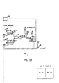
- LCD protection circuit 30 prevents damage to a passive LCD panel in the event of a system halt or a software bug.
- LCD protection circuit 30 enables clock and data buffers to the LCD panel when the VDD_enable register is set (when VDD is turned on). It then resets the VDD_enable register (turning VDD off), resets the VEE_enable register (turning VEE off), and disables the LCD clock and data buffers under either of the following conditions: (1) one of the clock signals stops transitioning; (2) one of the clocks has not started transitioning after a specified amount of time.
- the LCD protection circuit 30 allows widely configurable timing intervals. It will work with many different LCD controllers and passive displays, ranging from 320x200 to SVGA resolution, and it uses standard logic integrated circuits (ICs) and standard passive components. Furthermore, the LCD protection circuit 30 gives protection against LCD clocks/data being accidentally restarted after removal of LCD voltage supplies.
- the LCD protection circuit 30 may be used with a system having a CPU and an LCD controller.
- the LCD controller generates a row clock CL1, a dot clock CL2, a frame signal CLF, and data signals LCD[3:0], and provides these signals to an LCD panel.
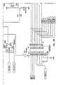
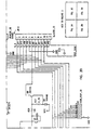
- the LCD protection circuit 30 includes one non-retriggerable monostable multivibrator 32 (or “one-shot 32"), two retriggersble one-shots 34 and 36, one D flip-flop 38, two OR gates 46 and 48, two AND gates 44 and 52, and a NAND gate 50, all connected substantially as shown.
- the timing resistor and capacitor values for the one shots have been chosen so that the one shot 32 produces a 0.1ms pulse and the one shots 34 and 36 produce 1.0ms pulses. It should be understood, however, that the timing resistor and capacitor values for the one shots may be changed without departing from the scope of the present invention.
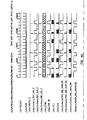
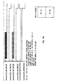
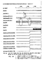
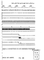
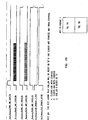
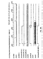
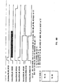
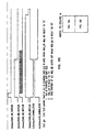
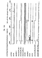
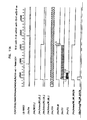
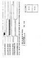
- the LCD protection circuit 30 will be discussed with reference to Figures 4-11.
- RESET occurs (e.g., generated by an external CPU)
- all three on-shots 32, 34, and 36 are cleared.
- the VDD_EN signal is used to enable the clock and data buffers (buffered signals include XCL1, XCL2, XCLF, XLCD[3:0]), so that they are transmitted only when VDD is enabled.
- the rising edge of VDD_EN triggers the one shot 32.
- This one-shot 32 generates a 0.1ms-long high pulse, VDD_PULSE.
- the VDD_PULSE signal enters the two OR gates 46 and 48, one with the buffered dot clock (XCL2), and the other with the buffered row clock (XCL1).
- the outputs of the OR gates 46 and 48 (CL2VDD and CL1VDD) are fed into the two one-shots 34 and 36.
- the one-shots 34 and 36 each generate an independent 1.0ms-long high pulse (CL2_PULSE and CL1_PULSE). These pulses are ANDed together and inverted by the NAND gate 50 to produce a low-going pulse ( CL1CL2 ). This low pulse is continued as long as both clocks continue to transition. However, if one clock stops transitioning for more than 2.0ms, or does not start to transition after a maximum of 2.0ms, the one shots 34 and 36 will time out and generate a rising edge on CL1CL2 .
- the rising edge of CL1CL2 clocks a D flip-flop 38, whose active-low output is ANDed with RESET by the AND gate 52 to reset the VDD_EN signal. Resetting the VDD_EN signal in turn disables the VDD supply, the clock and data buffers, and the VEE supply.
- the D flip-flop 38 should be cleared before the user can attempt to enable the LCD power supplies, or data again.
- TFT Thin Film Transistor
- One example use of the LCD protection circuit 30 is in a system such as that described in the data sheet entitled "Elentari Optimized 32-bit 486-class Controller With On-chip Peripherals for Embedded Systems", authored by National Semiconductor Corporation of Santa Clara, California.
- the system described therein is a single IC chip having an on-board CPU, LCD controller, and other on-board peripherals.
- a user should normally take care to power-up and power-down the LCD controller and the display panel in the proper sequence.
- other peripherals and internal functional blocks can be enabled and configured for normal operation fairly easily, but the LCD controller does normally require special handling. Because of the nature of the LCD panels, care must be taken in applying the high voltages used in the display panels themselves.
- VEE external DC power supplied to the LCD Display
- the power-up sequence is as follows: 1) Configure the LCD control registers; 2) Apply V DD (5V or 3V) to the display; 3) Enable the LCD clock from the power management registers - this should be done within 20 msec. of applying V DD ; 4) Enable the LCD controller; and, 5) Within 20 msec. max after applying the LCD clock, apply V EE (22V/-26V) to the display.
- the power-down sequence is as follows: 1) Remove V EE from the display; 2) Disable the LCD controller; 3) Within 20 msec. of removing V EE , disable the LCD clock; and, 4) Within 20 msec. of removing the LCD clock, remove V DD from the display.
- the LCD clock should not be disabled when the LCD is enabled.
Landscapes
- Engineering & Computer Science (AREA)
- Chemical & Material Sciences (AREA)
- Crystallography & Structural Chemistry (AREA)
- Physics & Mathematics (AREA)
- Computer Hardware Design (AREA)
- General Physics & Mathematics (AREA)
- Theoretical Computer Science (AREA)
- Control Of Indicators Other Than Cathode Ray Tubes (AREA)
- Liquid Crystal Display Device Control (AREA)
- Liquid Crystal (AREA)
Claims (10)
- Circuit pour protéger un afficheur à cristaux liquides contre une détérioration par une tension continue dans le cas d'un arrêt du système ou d'un bogue de logiciel, comportant
une première porte OU (46) recevant une première impulsion indiquant un début d'alimentation en une tension d'alimentation de l'afficheur à cristaux liquides, à une entrée, et un premier signal d'horloge fourni en même temps que des données d'affichage par cristaux liquides depuis un dispositif de commande extérieur, à l'afficheur à cristaux liquides, à une autre entrée,
une seconde porte OU (48) recevant la première impulsion indiquant le début de l'alimentation en tension d'alimentation pour les cristaux liquides à une entrée, et un second signal d'horloge fourni en même temps que les données d'affichage par cristaux liquides depuis le dispositif de commande extérieur pour l'afficheur à cristaux liquides, à une autre entrée,
un premier multivibrateur monostable (34), couplé à la première porte OU, qui reçoit un signal de sortie de la première porte OU et qui génère une seconde impulsion en réponse à ce signal ; et
un second multivibrateur monostable (36), couplé à la seconde porte OU, qui reçoit un signal de sortie de la seconde porte OU et génère une troisième impulsion en réponse à ce signal ; et
une première porte logique (50) couplée aux premier et second multivibrateurs monostables, qui génère une quatrième impulsion changeant d'état en réponse à l'arrêt des transitions de l'un des premier et second signaux d'horloge pendant une première période de temps prédéterminée, et invalide ainsi l'application de la tension d'alimentation, des données pour cristaux liquides et des premier et second signaux d'horloge à l'afficheur à cristaux liquides. - Circuit selon la revendication 1, dans lequel la quatrième impulsion change également d'état en réponse au fait que l'un des premier et second signaux d'horloge ne commence pas de transition pendant une seconde période de temps prédéterminée.
- Circuit selon la revendication 1, dans lequel la première porte logique comprend une porte NON-ET.
- Circuit selon la revendication 1, comportant en outre un troisième multivibrateur monostable (32) couplé aux première et seconde portes OU, qui reçoit un signal de validation et qui génère la première impulsion en réponse à ce signal.
- Circuit selon la revendication 4, dans lequel la quatrième impulsion est utilisée pour restaurer le signal de validation.
- Circuit selon la revendication 5, comportant en outre une première bascule (38), couplée à la'première porte logique, qui reçoit la quatrième impulsion et génère une cinquième impulsion utilisée pour restaurer le signal de validation.
- Circuit selon la revendication 1, dans lequel les premier et second multivibrateurs monostables sont des multivibrateurs monostables redéclenchables.
- Circuit selon l'une quelconque des revendications 4, 5 ou 6, comportant en outre un circuit tampon couplé de façon à recevoir le signal de validation qui génère les premier et second signaux d'horloge en réponse au signal de validation.
- Circuit selon l'une quelconque des revendications 4, 5 ou 6, comportant en outre une première porte ET (52) couplée à la première bascule, qui reçoit la quatrième impulsion et qui soumet à une opération ET la quatrième impulsion avec un signal de restauration utilisé pour restaurer le signal de validation.
- Circuit selon la revendication 4, dans lequel le troisième multivibrateur monostable est un multivibrateur non redéclenchable.
Applications Claiming Priority (3)
| Application Number | Priority Date | Filing Date | Title |
|---|---|---|---|
| US08/452,094 US5731812A (en) | 1995-05-26 | 1995-05-26 | Liquid crystal display (LCD) protection circuit |
| US452094 | 1995-05-26 | ||
| PCT/US1996/007585 WO1996037876A2 (fr) | 1995-05-26 | 1996-05-23 | Systeme de protection pour un affichage a cristaux liquides |
Publications (2)
| Publication Number | Publication Date |
|---|---|
| EP0772861A2 EP0772861A2 (fr) | 1997-05-14 |
| EP0772861B1 true EP0772861B1 (fr) | 2003-09-17 |
Family
ID=23795011
Family Applications (1)
| Application Number | Title | Priority Date | Filing Date |
|---|---|---|---|
| EP96920445A Expired - Lifetime EP0772861B1 (fr) | 1995-05-26 | 1996-05-23 | Systeme de protection pour un affichage a cristaux liquides |
Country Status (4)
| Country | Link |
|---|---|
| US (1) | US5731812A (fr) |
| EP (1) | EP0772861B1 (fr) |
| KR (1) | KR100388538B1 (fr) |
| WO (1) | WO1996037876A2 (fr) |
Cited By (1)
| Publication number | Priority date | Publication date | Assignee | Title |
|---|---|---|---|---|
| US9041640B2 (en) | 2011-12-12 | 2015-05-26 | Samsung Electronics Co., Ltd. | Display driver and manufacturing method thereof |
Families Citing this family (5)
| Publication number | Priority date | Publication date | Assignee | Title |
|---|---|---|---|---|
| KR0176429B1 (ko) * | 1996-02-28 | 1999-04-01 | 윤종용 | 엘시디 모듈의 직류 충격 예방 방법 |
| US6448962B1 (en) | 1999-05-14 | 2002-09-10 | Three-Five Systems, Inc. | Safety timer to protect a display from fault conditions |
| CA2526467C (fr) * | 2003-05-20 | 2015-03-03 | Kagutech Ltd. | Commande de retroaction recursive de face arriere numerique |
| TWI274312B (en) * | 2005-03-11 | 2007-02-21 | Benq Corp | A display with a display chip protection device |
| JP2018040963A (ja) * | 2016-09-08 | 2018-03-15 | ラピスセミコンダクタ株式会社 | 表示ドライバ及び表示装置 |
Family Cites Families (10)
| Publication number | Priority date | Publication date | Assignee | Title |
|---|---|---|---|---|
| JPS5849987A (ja) * | 1981-09-19 | 1983-03-24 | シャープ株式会社 | 表示駆動方式 |
| US4538197A (en) * | 1984-01-18 | 1985-08-27 | General Electric Company | Synchronism check relay |
| DE3807020A1 (de) * | 1988-03-04 | 1989-09-14 | Eurosil Electronic Gmbh | Fluessigkristallanzeige mit taktgesteuerter abschaltung |
| US5204953A (en) * | 1989-08-04 | 1993-04-20 | Intel Corporation | One clock address pipelining in segmentation unit |
| US5259006A (en) * | 1990-04-18 | 1993-11-02 | Quickturn Systems, Incorporated | Method for substantially eliminating hold time violations in implementing high speed logic circuits or the like |
| JPH04269707A (ja) * | 1991-02-26 | 1992-09-25 | Sanyo Electric Co Ltd | 液晶駆動回路 |
| JPH04366892A (ja) * | 1991-06-13 | 1992-12-18 | Seiko Instr Inc | 液晶ドライバ保護回路 |
| US5189319A (en) * | 1991-10-10 | 1993-02-23 | Intel Corporation | Power reducing buffer/latch circuit |
| US5254888A (en) * | 1992-03-27 | 1993-10-19 | Picopower Technology Inc. | Switchable clock circuit for microprocessors to thereby save power |
| US5404473A (en) * | 1994-03-01 | 1995-04-04 | Intel Corporation | Apparatus and method for handling string operations in a pipelined processor |
-
1995
- 1995-05-26 US US08/452,094 patent/US5731812A/en not_active Expired - Lifetime
-
1996
- 1996-05-23 KR KR1019970700547A patent/KR100388538B1/ko not_active Expired - Lifetime
- 1996-05-23 WO PCT/US1996/007585 patent/WO1996037876A2/fr not_active Ceased
- 1996-05-23 EP EP96920445A patent/EP0772861B1/fr not_active Expired - Lifetime
Cited By (1)
| Publication number | Priority date | Publication date | Assignee | Title |
|---|---|---|---|---|
| US9041640B2 (en) | 2011-12-12 | 2015-05-26 | Samsung Electronics Co., Ltd. | Display driver and manufacturing method thereof |
Also Published As
| Publication number | Publication date |
|---|---|
| WO1996037876A3 (fr) | 1997-02-06 |
| KR970705120A (ko) | 1997-09-06 |
| EP0772861A2 (fr) | 1997-05-14 |
| WO1996037876A2 (fr) | 1996-11-28 |
| US5731812A (en) | 1998-03-24 |
| KR100388538B1 (ko) | 2003-10-08 |
Similar Documents
| Publication | Publication Date | Title |
|---|---|---|
| US5008846A (en) | Power and signal supply control device | |
| US9383813B2 (en) | Dynamic control of reduced voltage state of graphics controller component of memory controller | |
| KR100430769B1 (ko) | 클럭 주파수 변환 회로 | |
| USRE39236E1 (en) | Flat panel device and display driver with on/off power controller used to prevent damage to the LCD | |
| US7190343B2 (en) | Liquid crystal display and driving method thereof | |
| US20040172565A1 (en) | Data processing apparatus | |
| JP2000172364A (ja) | 情報処理装置 | |
| JPH04211819A (ja) | 情報処理装置 | |
| KR20130107912A (ko) | 액정표시장치의 레벨 시프터 | |
| JP2000132263A (ja) | 集積回路及びコンピュ―タ・システム | |
| US5777611A (en) | Apparatus for controlling power sequence of an LCD module | |
| KR950000548B1 (ko) | 전원을 내장한 확장 유닛을 갖는 컴퓨터 시스템 | |
| US5434589A (en) | TFT LCD display control system for displaying data upon detection of VRAM write access | |
| US5731812A (en) | Liquid crystal display (LCD) protection circuit | |
| US5703629A (en) | Computer system including protected graphics display control signal sequencing | |
| WO1996037876A9 (fr) | Systeme de protection pour un affichage a cristaux liquides | |
| US6310599B1 (en) | Method and apparatus for providing LCD panel protection in an LCD display controller | |
| JPH0380318B2 (fr) | ||
| JP3411396B2 (ja) | コンピュータシステム | |
| DE69629992T2 (de) | Schutzschaltung für eine flüssigkristallanzeige | |
| JPH11142809A (ja) | 液晶表示装置 | |
| JP2000172363A (ja) | 情報処理装置 | |
| JP3369164B2 (ja) | 液晶表示素子 | |
| JP3487593B2 (ja) | 液晶表示素子 | |
| JP3369163B2 (ja) | 液晶表示素子 |
Legal Events
| Date | Code | Title | Description |
|---|---|---|---|
| PUAI | Public reference made under article 153(3) epc to a published international application that has entered the european phase |
Free format text: ORIGINAL CODE: 0009012 |
|
| AK | Designated contracting states |
Kind code of ref document: A2 Designated state(s): DE FR GB |
|
| PUAK | Availability of information related to the publication of the international search report |
Free format text: ORIGINAL CODE: 0009015 |
|
| AK | Designated contracting states |
Kind code of ref document: A3 Designated state(s): DE FR GB |
|
| 17P | Request for examination filed |
Effective date: 19970523 |
|
| 17Q | First examination report despatched |
Effective date: 20021114 |
|
| GRAH | Despatch of communication of intention to grant a patent |
Free format text: ORIGINAL CODE: EPIDOS IGRA |
|
| GRAS | Grant fee paid |
Free format text: ORIGINAL CODE: EPIDOSNIGR3 |
|
| GRAA | (expected) grant |
Free format text: ORIGINAL CODE: 0009210 |
|
| AK | Designated contracting states |
Kind code of ref document: B1 Designated state(s): DE FR GB |
|
| PG25 | Lapsed in a contracting state [announced via postgrant information from national office to epo] |
Ref country code: FR Free format text: LAPSE BECAUSE OF FAILURE TO SUBMIT A TRANSLATION OF THE DESCRIPTION OR TO PAY THE FEE WITHIN THE PRESCRIBED TIME-LIMIT Effective date: 20030917 |
|
| REG | Reference to a national code |
Ref country code: GB Ref legal event code: FG4D |
|
| REF | Corresponds to: |
Ref document number: 69629992 Country of ref document: DE Date of ref document: 20031023 Kind code of ref document: P |
|
| PGFP | Annual fee paid to national office [announced via postgrant information from national office to epo] |
Ref country code: GB Payment date: 20040519 Year of fee payment: 9 Ref country code: FR Payment date: 20040519 Year of fee payment: 9 |
|
| PLBE | No opposition filed within time limit |
Free format text: ORIGINAL CODE: 0009261 |
|
| STAA | Information on the status of an ep patent application or granted ep patent |
Free format text: STATUS: NO OPPOSITION FILED WITHIN TIME LIMIT |
|
| 26N | No opposition filed |
Effective date: 20040618 |
|
| EN | Fr: translation not filed | ||
| PG25 | Lapsed in a contracting state [announced via postgrant information from national office to epo] |
Ref country code: GB Free format text: LAPSE BECAUSE OF NON-PAYMENT OF DUE FEES Effective date: 20050523 |
|
| GBPC | Gb: european patent ceased through non-payment of renewal fee |
Effective date: 20050523 |
|
| PGFP | Annual fee paid to national office [announced via postgrant information from national office to epo] |
Ref country code: DE Payment date: 20120529 Year of fee payment: 17 |
|
| REG | Reference to a national code |
Ref country code: DE Ref legal event code: R082 Ref document number: 69629992 Country of ref document: DE |
|
| PG25 | Lapsed in a contracting state [announced via postgrant information from national office to epo] |
Ref country code: DE Free format text: LAPSE BECAUSE OF NON-PAYMENT OF DUE FEES Effective date: 20131203 |
|
| REG | Reference to a national code |
Ref country code: DE Ref legal event code: R119 Ref document number: 69629992 Country of ref document: DE Effective date: 20131203 |