EP0773465A2 - Arrangement mécanique et contrÔle thermique d'une matrice plate à miroirs - Google Patents
Arrangement mécanique et contrÔle thermique d'une matrice plate à miroirs Download PDFInfo
- Publication number
- EP0773465A2 EP0773465A2 EP96306422A EP96306422A EP0773465A2 EP 0773465 A2 EP0773465 A2 EP 0773465A2 EP 96306422 A EP96306422 A EP 96306422A EP 96306422 A EP96306422 A EP 96306422A EP 0773465 A2 EP0773465 A2 EP 0773465A2
- Authority
- EP
- European Patent Office
- Prior art keywords
- liquid crystal
- substrate holder
- substrate
- reflective
- wiring board
- Prior art date
- Legal status (The legal status is an assumption and is not a legal conclusion. Google has not performed a legal analysis and makes no representation as to the accuracy of the status listed.)
- Granted
Links
Images


Classifications
-
- G—PHYSICS
- G02—OPTICS
- G02F—OPTICAL DEVICES OR ARRANGEMENTS FOR THE CONTROL OF LIGHT BY MODIFICATION OF THE OPTICAL PROPERTIES OF THE MEDIA OF THE ELEMENTS INVOLVED THEREIN; NON-LINEAR OPTICS; FREQUENCY-CHANGING OF LIGHT; OPTICAL LOGIC ELEMENTS; OPTICAL ANALOGUE/DIGITAL CONVERTERS
- G02F1/00—Devices or arrangements for the control of the intensity, colour, phase, polarisation or direction of light arriving from an independent light source, e.g. switching, gating or modulating; Non-linear optics
- G02F1/01—Devices or arrangements for the control of the intensity, colour, phase, polarisation or direction of light arriving from an independent light source, e.g. switching, gating or modulating; Non-linear optics for the control of the intensity, phase, polarisation or colour
- G02F1/13—Devices or arrangements for the control of the intensity, colour, phase, polarisation or direction of light arriving from an independent light source, e.g. switching, gating or modulating; Non-linear optics for the control of the intensity, phase, polarisation or colour based on liquid crystals, e.g. single liquid crystal display cells
- G02F1/133—Constructional arrangements; Operation of liquid crystal cells; Circuit arrangements
- G02F1/1333—Constructional arrangements; Manufacturing methods
- G02F1/133382—Heating or cooling of liquid crystal cells other than for activation, e.g. circuits or arrangements for temperature control, stabilisation or uniform distribution over the cell
- G02F1/133385—Heating or cooling of liquid crystal cells other than for activation, e.g. circuits or arrangements for temperature control, stabilisation or uniform distribution over the cell with cooling means, e.g. fans
-
- G—PHYSICS
- G02—OPTICS
- G02F—OPTICAL DEVICES OR ARRANGEMENTS FOR THE CONTROL OF LIGHT BY MODIFICATION OF THE OPTICAL PROPERTIES OF THE MEDIA OF THE ELEMENTS INVOLVED THEREIN; NON-LINEAR OPTICS; FREQUENCY-CHANGING OF LIGHT; OPTICAL LOGIC ELEMENTS; OPTICAL ANALOGUE/DIGITAL CONVERTERS
- G02F1/00—Devices or arrangements for the control of the intensity, colour, phase, polarisation or direction of light arriving from an independent light source, e.g. switching, gating or modulating; Non-linear optics
- G02F1/01—Devices or arrangements for the control of the intensity, colour, phase, polarisation or direction of light arriving from an independent light source, e.g. switching, gating or modulating; Non-linear optics for the control of the intensity, phase, polarisation or colour
- G02F1/13—Devices or arrangements for the control of the intensity, colour, phase, polarisation or direction of light arriving from an independent light source, e.g. switching, gating or modulating; Non-linear optics for the control of the intensity, phase, polarisation or colour based on liquid crystals, e.g. single liquid crystal display cells
- G02F1/133—Constructional arrangements; Operation of liquid crystal cells; Circuit arrangements
- G02F1/1333—Constructional arrangements; Manufacturing methods
- G02F1/133308—Support structures for LCD panels, e.g. frames or bezels
-
- G—PHYSICS
- G02—OPTICS
- G02F—OPTICAL DEVICES OR ARRANGEMENTS FOR THE CONTROL OF LIGHT BY MODIFICATION OF THE OPTICAL PROPERTIES OF THE MEDIA OF THE ELEMENTS INVOLVED THEREIN; NON-LINEAR OPTICS; FREQUENCY-CHANGING OF LIGHT; OPTICAL LOGIC ELEMENTS; OPTICAL ANALOGUE/DIGITAL CONVERTERS
- G02F1/00—Devices or arrangements for the control of the intensity, colour, phase, polarisation or direction of light arriving from an independent light source, e.g. switching, gating or modulating; Non-linear optics
- G02F1/01—Devices or arrangements for the control of the intensity, colour, phase, polarisation or direction of light arriving from an independent light source, e.g. switching, gating or modulating; Non-linear optics for the control of the intensity, phase, polarisation or colour
- G02F1/13—Devices or arrangements for the control of the intensity, colour, phase, polarisation or direction of light arriving from an independent light source, e.g. switching, gating or modulating; Non-linear optics for the control of the intensity, phase, polarisation or colour based on liquid crystals, e.g. single liquid crystal display cells
- G02F1/133—Constructional arrangements; Operation of liquid crystal cells; Circuit arrangements
- G02F1/136—Liquid crystal cells structurally associated with a semi-conducting layer or substrate, e.g. cells forming part of an integrated circuit
-
- G—PHYSICS
- G02—OPTICS
- G02F—OPTICAL DEVICES OR ARRANGEMENTS FOR THE CONTROL OF LIGHT BY MODIFICATION OF THE OPTICAL PROPERTIES OF THE MEDIA OF THE ELEMENTS INVOLVED THEREIN; NON-LINEAR OPTICS; FREQUENCY-CHANGING OF LIGHT; OPTICAL LOGIC ELEMENTS; OPTICAL ANALOGUE/DIGITAL CONVERTERS
- G02F1/00—Devices or arrangements for the control of the intensity, colour, phase, polarisation or direction of light arriving from an independent light source, e.g. switching, gating or modulating; Non-linear optics
- G02F1/01—Devices or arrangements for the control of the intensity, colour, phase, polarisation or direction of light arriving from an independent light source, e.g. switching, gating or modulating; Non-linear optics for the control of the intensity, phase, polarisation or colour
- G02F1/13—Devices or arrangements for the control of the intensity, colour, phase, polarisation or direction of light arriving from an independent light source, e.g. switching, gating or modulating; Non-linear optics for the control of the intensity, phase, polarisation or colour based on liquid crystals, e.g. single liquid crystal display cells
- G02F1/133—Constructional arrangements; Operation of liquid crystal cells; Circuit arrangements
- G02F1/1333—Constructional arrangements; Manufacturing methods
- G02F1/133308—Support structures for LCD panels, e.g. frames or bezels
- G02F1/133322—Mechanical guidance or alignment of LCD panel support components
-
- G—PHYSICS
- G02—OPTICS
- G02F—OPTICAL DEVICES OR ARRANGEMENTS FOR THE CONTROL OF LIGHT BY MODIFICATION OF THE OPTICAL PROPERTIES OF THE MEDIA OF THE ELEMENTS INVOLVED THEREIN; NON-LINEAR OPTICS; FREQUENCY-CHANGING OF LIGHT; OPTICAL LOGIC ELEMENTS; OPTICAL ANALOGUE/DIGITAL CONVERTERS
- G02F1/00—Devices or arrangements for the control of the intensity, colour, phase, polarisation or direction of light arriving from an independent light source, e.g. switching, gating or modulating; Non-linear optics
- G02F1/01—Devices or arrangements for the control of the intensity, colour, phase, polarisation or direction of light arriving from an independent light source, e.g. switching, gating or modulating; Non-linear optics for the control of the intensity, phase, polarisation or colour
- G02F1/13—Devices or arrangements for the control of the intensity, colour, phase, polarisation or direction of light arriving from an independent light source, e.g. switching, gating or modulating; Non-linear optics for the control of the intensity, phase, polarisation or colour based on liquid crystals, e.g. single liquid crystal display cells
- G02F1/133—Constructional arrangements; Operation of liquid crystal cells; Circuit arrangements
- G02F1/1333—Constructional arrangements; Manufacturing methods
- G02F1/133308—Support structures for LCD panels, e.g. frames or bezels
- G02F1/133325—Assembling processes
Definitions
- the present invention relates to the construction, mechanical packaging, and thermal management of flat mirror arrays for reflection projection displays, and more specifically to the assembly of substantially flat liquid crystal semiconductor spatial light monitors on a surface, in alignment with the optical and electrical components and such thermal sinking devices as are necessary for use with liquid crystal display elements.
- a generalized liquid crystal display consists of a source of light, having frequency components of the full visible spectrum, which is directed at a series of filters which separate the light into red, blue, and green component beams.
- the component beams are then directed to interact with an optically reactive liquid crystal medium, which alters the component beams in accordance with specific image information.
- the altered beams are reconstituted and either transmitted directly onto a screen, or may be projected through a lens.
- transmissive liquid crystal element a quantity of an electrically active liquid crystal medium is positioned between a pair of spaced optically transparent surfaces.
- Each of the transparent surfaces further includes an inner surface electrode which permits the application of a voltage across the liquid crystal, therein altering the optical characteristics of the medium, for example, from transparent to absorptive (or scattering) in the frequency of the specific beam. It is understood that the image information necessary to provide a meaningful picture is provided by the appropriate variation of the voltage across the element.
- Reflective liquid crystal elements are similar to transmissive ones, but for the fact that only one of the spaced surfaces is optically transmissive. The other surface is reflective. In such an element the component beam of light is directed through the transmissive surface and the liquid crystal, reflects off the far reflective surface, passes back again through the liquid crystal medium and the transmissive surface, and thereby may be properly encoded with image information in accordance by variance of the transmissive state of the liquid crystal.
- cooling means must be provided.
- U.S. Patent No. 5,170,195 to Akiyama et al. teaches a cooling device comprising a container filled with a liquid coolant fluid and outwardly extending heat fins.
- the container which is constructed of transparent materials, is disposed in contact with the face of a liquid crystal display element, therein receiving the heat from the element and providing a cooling effect therefor.
- Such a cooling system is considerably more bulky than would be otherwise desired.
- the manufacturing of such a device necessitates substantially more complexity than is desirable for a competitively marketed display system.
- U.S. Patent No. 5,170,1945, to Kurematsu et al. comprises a liquid crystal display element, which is a reflective type, consisting of a top optically transmissive surface, a quantity of voltage sensitive liquid crystal material, and a rear reflective surface which forms the front surface of a heat sink element.
- the reflective surface of the reflective liquid crystal element is the aluminum surface of a heat sink element. The cooling of the element is, therefore, provided directly to the liquid crystal by virtue of its contact with the heat sink.
- CMOS technology has been identified as an ideal fabrication method for constructing the high performance transistor arrays, which entails the building up of material on the surface of high quality single crystal silicon.
- Lattice mismatching, as well as thermal expansion characteristics can generate significant stresses in the underlying substrate material (the silicon), therein causing significant bowing of the mirrored surface.
- the bowing which translates to a non-planarity of the surface, causes both (1) a non-uniform thickness of the liquid crystal layer between the bowed reflective surface and the planar transmissive top layer, and (2) variations in the path length of the reflected light from different parts of the element, and of the array. These effects compromise the electro-optic properties of the elements and/or array.
- a reflective liquid crystal display element having a substantially flat mirror surface, a corresponding uniform liquid crystal, a separately mounted thermal heat sink, and an enhanced packaging so that the elements may be set forth in an array which is properly aligned with optical elements associated therewith.
- this invention teaches a structure comprising a semiconductor substrate, for example a silicon wafer, having circuitry disposed on the surface thereof, which has formed thereon an optically reflective surface layer.
- the semiconductor may be diced into a multiplicity of properly sized elements, each of which is laminated to an optically flat surface.
- the lamination of the mirrored semiconductor elements is preferably done with a spin-on or spray-on liquid adhesive which cures in place, or alternatively with an adhesive film.
- the joint must be capable of both surviving all such thermal cycles and solvent treatments as are necessary to fabricate the liquid crystal element, and efficiently transferring heat such that the temperature gradient associated with the cooling means (such as are described hereinafter) is sufficiently small, therein protecting the functionality of the liquid crystal.
- the substrate is preferably chosen to have a similar coefficient of thermal expansion.
- An ideally suitable material for the optically flat surface, for use with a silicon semiconductor substrate, is polished ground glass. Ceramic, silicon, or metal substrate materials may also be used as the optically flat substrate.
- the preparation of the substrate as described above provides a flat surface onto which the liquid crystal is disposed.
- the spacing of a flat transmissive layer, such as glass, in parallel alignment with the substrate layer provides a uniformly thick region of liquid crystal. This uniform thickness is provided by an accurately positioned edge seal which secures the substrate and the transmissive top layer together in spaced relation to one another.
- the present invention further comprises a substrate holder on which the liquid crystal element rests. Any gaps between the holder and the element are filled with a thermal paste.
- an array of multiple liquid crystal elements is required in order to reproduce a complex image, for example a high definition television picture, or a complex video display screen.
- an alignment fixture is coupled to the entire array (or a portion thereof) to ensure that the elements are properly aligned to the optics. Once the elements are properly aligned, the means for securing the substrate holders to the wiring board are fully tightened, and the fixture is removed. Once fully connected and positioned, heat sinks are attached to the rear of the substrate holder.
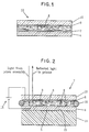
- Figure 1 is a side cross-section conceptual view of a reflective liquid crystal display element.
- Figure 2 is a side cross-sectional view of the reflective liquid crystal display structure of the present invention wherein the mirror array is joined to an optically flat substrate.
- Figure 3 is a perspective view of a substrate holder of the present invention.
- Figure 4 is a side cross-section view of the element, substrate, and substrate holder mounted to a wiring board, wherein a heat sink is coupled to the rear of the assembly.
- Figure 5 is a perspective view of the wiring board, having the substrate holder loosely mounted thereto, therein corresponding to one step of the assembly process.
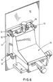
- Figure 6 is a perspective view of the wiring board wherein a mounting and alignment fixture is shown coupled to the rear of thereof for properly orienting the element relative to associated optical devices, in accordance with another step in the assembly process of the present invention.
- Figure 7 is an exploded view of a top perspective of another alignment fixture which is an aspect of the present invention.
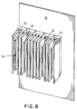
- Figure 8 is a view of the heat sink mounted to the rear of the substrate holder, in accordance with the structure and assembly process of the present invention.
- FIG. 1 a side cross-section conceptual view of a reflective liquid crystal display element 12, is shown.
- a reflective layer 2 is deposited on a base material 4, which provides a backing for the reflective layer 2.
- the backing layer 4 further comprises microcircuitry for providing a voltage, as will be more fully set forth below with respect to Figure 2. It is desirable that the reflective layer 2 comprise a conductive material. If the reflective layer 2 is not conductive, it is necessary to provide a transparent conductive layer (not shown) across the reflective surface.
- liquid crystal fluid medium 6 which is electro-optically active.
- one type of liquid crystal medium 6 permits the polarized light to be reflected without any rotation of the polarization orientation when there is an absence of voltage thereacross, and reflects the light and rotates the polarization when a given voltage is applied thereacross.
- the displayed image may selectively presented as bright or dark depending upon which polarization the analyzer allows to pass.
- the incident light may be diffusely scattered in correspondence with the application of a voltage while permitting the light to go through when no voltage is applied.
- This liquid crystal layer 6 is generally maintained at a specific thickness, as described more fully hereinbelow, also with respect to Figure 2, so as to ensure constant optical properties and effects across the breadth of the element.
- the transparent conductive layer 8 may be a separate and distinct material, such as a conductive polymer, however, it is preferable that the layer 8 comprise an electrically conductive oxide formed on the bottom side of the transparent insulator layer 10.
- each of the element 12 corresponds to one of three colours: green, blue, or red.
- the composite of three images, each of a different colour are provided, therein forming a full colour image.
- FIG 2 shows a side cross-sectional view of the specific structure 7 of the present invention, which ensures that the underlying backing layer, which in this embodiment is a semiconductor wafer 4 having circuitry disposed thereon (not shown), remains uniformly flat is herein described.
- the wafer 4 has front and rear surfaces 3 and 5 respectively.
- a reflective layer 2 in the form of mirror pixels, on the front surface 3 of the semiconductor wafer 4
- the wafer is diced to the required dimensions and laminated to a substrate 14 having an optically flat surface 15 to give the global flatness to the array.
- the substrate 14 must be sufficiently rigid to resist out-of-plane distortion of the wafer 4.
- the lamination of the wafer 4 to the optically flat substrate 14 may be achieved by a variety of means, however, in a preferred embodiment the lamination is provided by a spin-on or spray-on liquid adhesive layer that cures in place by light or heat such that additional fabrication steps are not required beyond the joining of the wafer 4 to the substrate 14. It is further understood that the joining means must be capable of surviving all of the thermal cycles and solvent treatments associated with the subsequent manufacture of a liquid crystal element.
- Preferred optically flat substrates 14 include, but are not limited to, ground polished glass, wherein the thermal expansion coefficient of the glass is equivalent to that of the wafer 4. In alternative designs, it may be preferable to use polished metal or ceramic materials as the substrate. It is further understood, that thick and rigid silicon may be utilized as a substrate material as well.
- a particularly suitable example of the proper fabrication of the structure described above comprises laminating a bowed silicon wafer 4 to a polished flat glass substrate with a thermosetting adhesive.
- the lamination is preferably carried out in a gas pressure cell where uniform gas pressure is applied over the whole surface at 200 degrees centigrade.
- the degree of flatness of the reflective layer 2 on the surface of the wafer 4 may be maintained within the required tolerances for the intended liquid crystal application.
- an edge sealing material 18 is disposed such that the liquid crystal 6 may be applied to the reflective surface in partitioned spacings.
- the sealing material 18 supports and secures to the conductive and insulative transparent layers 8,10, respectively, with the liquid crystal in between, therein holding the element together.
- the spacing of the transparent layers 8,10 from the reflective layer 2 must also be maintained at proper distance tolerances such that the liquid crystal layer has a uniform depth across the array. In other words, the reflective layer 2 and the transparent layers 8,10 must be substantially parallel to one another.
- the uniform thickness of the liquid crystal is critical to the proper performance of the display element because of two factors. The first is that the optical path of the incident light through, and back through, the liquid crystal layer must be the same distance at all points along the array in order to prevent non-symmetric angulation of the beams at the optical elements which merge the mono-chromatic beams together.
- the second factor compelling the maintenance of a constant thickness through the liquid crystal layer 6 is that the electro-optical characteristics of the liquid crystal are directly related to the voltage applied thereacross. Voltage is applied across the liquid crystal via terminals of an external voltage source 16, coupled to the conductive transparent layer 8 and the microcircuitry imprinted on the wafer 4.
- an alignment and support structure which includes a substrate holder 20 is shown.
- the substrate holder 20 comprises a dish-like structure having a square perimeter conformation, wherein the interior 22 of the region is thinner than the perimeter.
- the four elongate sides 24 of the structure include regularly spaced screw holes 26 for mounting of the holder 20, and the structure 7 therein, to a wiring board (as described more fully with respect to Figure 5).
- a plurality of support pads 28 on which the structure 7 is designed to rest.
- three support pads 28 have been chosen, therein providing the ideal number of points on which to define planarity of the surface.
- the substrate holder 20 is ideally made of a good heat conducting material, such as a metal, so that the structure 7 will not be insulated as it builds up heat.
- the gap formed by the pads 28 between the substrate and the substrate holder is filled with a thermal paste which further increases the rate at which the dissipated power within the element can be removed by heat sinking means (as described more fully hereinbelow with respect to Figure 4).
- FIG 4 a cross-sectional view of the liquid crystal display element 12 and the substrate holder 20 having a heat sink device 30 coupled to the rear side of the holder 20, and being mounted to a wiring board 40 is provided.
- the element 12 is disposed on the optically flat substrate 14, which is in turn coupled to the substrate holder 20 via an adhesive thermal paste 32.
- the substrate holder 20 is coupled to a wiring board 40 by a set of coupling screws 34 which are disposed through the wiring board into the screw holes 26 of the holder 20.
- the wiring board includes cut-out sections formed therein (see Figure 5), about which the substrate holders 20 are coupled, and in which cut-out sections the display elements 12 are positioned so that they are in light receiving position with the remainder of the optical elements in the display device.
- the wiring board 40 is shown, having a liquid crystal element 12 mounted in a cut-out section 42 thereof, is shown in a perspective view.
- the region of the wiring board 40 which is adjacent to the cut-out section 42 includes a plurality of electrical connection pads to which the proper electrical connections (not shown) may be made to provide coupling to the driver chips 44 to drive the element 12.
- screw holes 46 are further provided which are mateable to the substrate holder 20 by screws 34, as described above.
- the driver chips 44 are first attached to the semiconductor wafer 4 which is known in the art. Then, the element 12, with driver chips 44 attached, must be precisely oriented on the wiring board 40. In this aligned position the electrical connection of the driver chips 44 to the wiring board 40 is made.
- an alignment fixture 50 which is mountable to the rear of the substrate holder 20, as described above, is shown in a perspective view using the alignment fixture 50 while holding the wiring board 40 stationary. Once the substrate holder 20 and the element 12 mounted therein with driver chips 44 attached have been placed against the wiring board 40, with the driver chips 44 aligned to the electrical connection pads on wiring board 40.
- the alignment fixture 50 may be of a slightly different configuration depending on the configuration of the device forming the electrical connections. For example, the wiring board and element assembly may be held horizontally instead of vertically, as shown, or the assembly fixture may contain rotary capability.
- the screws 34 which secure the substrate holder 20 to the wiring board 40 are kept loose, such that the element may be set to its ideal alignment. Once the alignment fixture 50 has been used to properly orient the elements, the screws 34 may be tightened to secure the substrate 20 in the ideal position.
- each assembly of liquid crystal elements 12 with driver chips 44 and wiring board 40 attached (shown as element 54 in Figure 5) must be precisely oriented to the projection optics. With an alignment fixture 50 attached to each of the several assemblies 54, such alignment can be achieved.
- the assembly can be attached in this aligned position to a mounting structure (not shown) by means of screws 52 (or other suitable releasable mounting means) through holes 56 in the substrate holder 20 and holes 46 in the wiring board 40. It is understood that holes 56 and each corresponding hole 46 are nominally aligned to each other to form individual holes through the substrate holder and wiring board through which a screw may be passed through both elements. It is further understood that there is sufficient clearance between the holes and screws so that small motions of alignment of the assembly 54 can be accommodated while still being able to attach the assembly to a mounting structure in its aligned position by means of the screws 54.
- alignment fixture 50 may be of a different configuration that shown depending on the mounting structure used and the requirements of the particular application.
- the alignment fixture 50 used for alignment of the electrical connections described above may also be a separate structure from the alignment fixture used to align an assembly 54 to remote optical elements.
- FIG. 7 a robust alignment fixture 100 for properly orienting the liquid crystal elements 12 with respect to one another such that the images which they project are superimposed on each other to form a single image is shown. It is understood, as stated above, that this proper orientation may be achieved with the use of an alignment fixture which can alter the position of the elements 12 in the horizontal direction, the vertical direction, and may further impart a rotation to the element. It is further understood that in order to ensure that the images are in focus requires that the fixture have another three degrees of freedom with respect to altering the position of the element 12; more specifically, the additional degrees of motion being translation perpendicular to the plane of the element, as well as azimuthal and elevational tilting. In addition, it is desirable that the alignment fixture 100 be stable over a range of temperatures and be able to withstand a level of mechanical shock and stress without deviating from its proper functionality.
- the liquid crystal element 12 and substrate holder 20 which are mounted to the wiring board 40 are releasably attached to the alignment fixture 100 by means of an adapter plate 102.
- An aligner base plate 104 is coupled to the adapter plate 102 in a similar manner, which is, more specifically, the receipt of pitched aligning studs 107 through the through holes 56 of the substrate holder, and alignment holes 103 and 109 of the adapter plate 102 and the aligner base plate 104, respectively.
- the studs 107 include an external threading, and may either be independently rotatable or may be coupleable to a nut 112 for relative adjustment.
- the aligner base plate 104 comprises three eccentric levers 105, which are closely confined within receiving slots 106, and which are rotatable through an angle bounded by the receiving slots 106. Appropriate manipulation of the levers 105 alters the position of the adapter plate 102, and the substrate holder 20 beneath, therein providing for image superposition relative to other elements 12. Once properly aligned in this manner, the adjustment is locked into place by means of screws 108.
- the pitched aligning studs 107 are coupled to a prism assembly 110 such that manipulation of the studs 107 (or the corresponding nuts 112) alters the relative spacing of the prism 110 and the liquid crystal element 12.
- eccentric manipulation of the studs 107 provides azimuthal and/or elevational tilting.
- the focus alignment may be locked in place by means of clamps 111 which are attached to the aligner base plate 104.
- this alignment fixture 100 has inherent desirable thermal properties in that it is first attached to the prism assembly 110 via very short paths, i.e. the pitched alignment studs 107. Such a short path minimizes the magnitude of thermal expansion.
- the prism assembly 110 and the plurality of liquid crystal element assemblies attached thereto form a symmetrical structure which allows thermal effects to be distributed evenly over the plurality, thus again minimizing the distortional and misaligning effects of thermal expansion.
- the rear surface of the wiring board 40 is shown, with the heat sink 30 coupled to the back of the substrate holder 20, as was illustrated in a side view in Figure 4.
- the heat sink 30 is coupled to the rear of the wiring board 40, after the proper positioning of the assembly 54, via screws 52.
- the holes in the wiring board 40, through which the screws 38 are placed, may be the same as the holes as were utilized to couple the alignment fixture 50 thereto, otherwise a separate set of holes may be provided.
- the process of fabrication, assembly, and alignment, therefore, of the above described structure, comprise a plurality of steps.
- the process of fabricating the structure 7 itself comprises: (1) forming the appropriate microcircuitry on the surface of a semiconductor wafer; (2) forming an array of reflective pixels on top of the microcircuitry; (3) attaching the bottom of the wafer, or portions thereof, to an optically flat substrate; (4) forming edge seals on the top surface of the wafer; (5) providing a uniformly thick layer of electro-optically active liquid crystal on the top of the wafer; (6) positioning a transparent conductive layer, in substantially parallel relationship to the reflective surface; and (7) positioning a transparent insulative layer on top of the transparent conductive layer.
- the process of assembling and aligning the structure 7, once fabricated, with the remaining optical and electrical elements of the display device comprises: (1) attaching driver chips and/or flexible circuitry to the semiconductor wafer; (2) attaching the element to a substrate holder; (3) loosely mounting the substrate holder to a wiring board, such that the structure is positioned in a cut-out section of the board; (4) utilizing an adjustment fixture, aligning the driver chips and/or flexible circuitry to the bonding pads on the wiring board; (5) connecting the driver chips and/or flexible circuitry to the wiring board; (6) tightening the mounts of the substrate holder to the wiring board; (7) utilizing another adjustment fixture, temporarily mounted in contact with the element, the substrate holder, and the wiring board, for the purpose of adjusting the relative orientation of the liquid crystal element with respect to the other optical elements of the device; (8) attaching the assembly to a mounting device; and (9) coupling a heat sink to the rear of the substrate holder for the purposes of dissipating as much of the thermal build-up in the element as
Landscapes
- Physics & Mathematics (AREA)
- Nonlinear Science (AREA)
- Mathematical Physics (AREA)
- Chemical & Material Sciences (AREA)
- Crystallography & Structural Chemistry (AREA)
- General Physics & Mathematics (AREA)
- Optics & Photonics (AREA)
- Engineering & Computer Science (AREA)
- Microelectronics & Electronic Packaging (AREA)
- Liquid Crystal (AREA)
- Devices For Indicating Variable Information By Combining Individual Elements (AREA)
Applications Claiming Priority (2)
| Application Number | Priority Date | Filing Date | Title |
|---|---|---|---|
| US08/540,860 US5721602A (en) | 1995-10-11 | 1995-10-11 | Mechanical packaging and thermal management of flat mirror arrays |
| US540860 | 1995-10-11 |
Publications (3)
| Publication Number | Publication Date |
|---|---|
| EP0773465A2 true EP0773465A2 (fr) | 1997-05-14 |
| EP0773465A3 EP0773465A3 (fr) | 1997-08-20 |
| EP0773465B1 EP0773465B1 (fr) | 2004-12-08 |
Family
ID=24157234
Family Applications (1)
| Application Number | Title | Priority Date | Filing Date |
|---|---|---|---|
| EP96306422A Expired - Lifetime EP0773465B1 (fr) | 1995-10-11 | 1996-09-04 | Arrangement mécanique et contrôle thermique d'une matrice plate à miroirs |
Country Status (5)
| Country | Link |
|---|---|
| US (2) | US5721602A (fr) |
| EP (1) | EP0773465B1 (fr) |
| JP (1) | JP3501329B2 (fr) |
| DE (1) | DE69633998T2 (fr) |
| ID (1) | ID18915A (fr) |
Cited By (2)
| Publication number | Priority date | Publication date | Assignee | Title |
|---|---|---|---|---|
| EP0911676A3 (fr) * | 1997-10-24 | 2000-01-12 | Canon Kabushiki Kaisha | Panneau à cristal liquide et projecteur à cristal liquide l'utilisant |
| EP1066547A4 (fr) * | 1998-03-24 | 2004-05-06 | Aurora Sys Inc | Dispositif de reglage de convergence mecanique et procede associe |
Families Citing this family (28)
| Publication number | Priority date | Publication date | Assignee | Title |
|---|---|---|---|---|
| JPH09166790A (ja) * | 1995-09-13 | 1997-06-24 | Canon Inc | 表示装置 |
| JPH10133590A (ja) * | 1996-10-28 | 1998-05-22 | Nitto Denko Corp | 発光表示装置 |
| US6501641B1 (en) | 1998-10-23 | 2002-12-31 | Lg. Philips Lcd Co. Ltd. | Portable computer having a flat panel display device |
| US5969783A (en) * | 1998-12-11 | 1999-10-19 | National Semiconductor Corporation | Reflective liquid crystal display and connection assembly and method |
| US6384890B1 (en) | 1999-11-15 | 2002-05-07 | National Semiconductor Corporation | Connection assembly for reflective liquid crystal projection with branched PCB display |
| US6307603B1 (en) * | 2000-01-18 | 2001-10-23 | Aurora Systems, Inc. | Low stress packaging for a display device |
| JP2001290434A (ja) * | 2000-04-04 | 2001-10-19 | Nec Corp | 表示装置 |
| USD454565S1 (en) | 2001-01-16 | 2002-03-19 | Display Werks, Inc. | Display housing |
| US6731354B2 (en) | 2001-03-22 | 2004-05-04 | Aurora Systems, Inc. | Liquid crystal display mount including a frame having stress relief recess |
| JP2003149629A (ja) * | 2001-06-01 | 2003-05-21 | Japan Aviation Electronics Industry Ltd | 液晶表示装置 |
| JP4217394B2 (ja) * | 2001-08-22 | 2009-01-28 | シャープ株式会社 | 液晶表示装置 |
| JP2003066404A (ja) * | 2001-08-27 | 2003-03-05 | Sony Corp | 液晶プロジェクタ |
| US20050073639A1 (en) * | 2003-10-06 | 2005-04-07 | Shin-Tung Pan | Heat dissipating structure of liquid crystal display |
| KR100710169B1 (ko) * | 2003-12-26 | 2007-04-20 | 엘지.필립스 엘시디 주식회사 | 액정 표시 장치의 제조 라인 및 제조 방법 |
| JPWO2005088711A1 (ja) * | 2004-03-16 | 2008-01-31 | 松下電器産業株式会社 | ドライバモジュール構造 |
| JP4701642B2 (ja) * | 2004-07-05 | 2011-06-15 | 日本電気株式会社 | 表示装置 |
| JP4706206B2 (ja) * | 2004-08-18 | 2011-06-22 | ソニー株式会社 | 放熱装置及び表示装置 |
| TWI263836B (en) * | 2004-11-12 | 2006-10-11 | Coretronic Corp | Heat dissipation method of display backlight unit and the structure thereof |
| JP2006258883A (ja) * | 2005-03-15 | 2006-09-28 | Seiko Epson Corp | 電気光学装置、電気光学装置の製造方法 |
| US20060221610A1 (en) * | 2005-04-01 | 2006-10-05 | Chew Tong F | Light-emitting apparatus having a plurality of overlapping panels forming recesses from which light is emitted |
| KR100713132B1 (ko) * | 2005-05-27 | 2007-05-02 | 삼성전자주식회사 | 프로젝터 |
| US20110181797A1 (en) * | 2008-09-01 | 2011-07-28 | Lensvector Inc. | Wafer-level fabrication of liquid crystal optoelectronic devices |
| JP5487704B2 (ja) * | 2009-04-27 | 2014-05-07 | セイコーエプソン株式会社 | 電気光学装置及び電子機器 |
| KR101588894B1 (ko) * | 2009-07-28 | 2016-01-27 | 엘지디스플레이 주식회사 | 액정표시장치 |
| KR102115174B1 (ko) * | 2012-06-18 | 2020-05-27 | 삼성디스플레이 주식회사 | 표시 패널 |
| US9762868B2 (en) | 2013-06-28 | 2017-09-12 | Thomson Licensing | Highlighting an object displayed by a pico projector |
| JP6274130B2 (ja) * | 2015-02-27 | 2018-02-07 | 株式会社Jvcケンウッド | 反射型液晶パネル装置及び反射型液晶パネル装置体 |
| CN209979938U (zh) | 2018-08-28 | 2020-01-21 | 苹果公司 | 可佩戴的头戴式显示器和可佩戴的显示系统 |
Family Cites Families (29)
| Publication number | Priority date | Publication date | Assignee | Title |
|---|---|---|---|---|
| US3374537A (en) * | 1965-03-22 | 1968-03-26 | Philco Ford Corp | Method of connecting leads to a semiconductive device |
| US4025942A (en) * | 1974-03-18 | 1977-05-24 | Kulite Semiconductor Products, Inc. | Low pressure transducers employing large silicon diaphragms having non-critical electrical properties |
| JPS5717281A (en) * | 1980-07-04 | 1982-01-28 | Matsushita Electric Ind Co Ltd | Display panel for liquid crystal television |
| EP0055317B1 (fr) * | 1980-12-31 | 1985-09-25 | International Business Machines Corporation | Module d'affichage électrochrome et système réflecteur de projection |
| US4470856A (en) * | 1983-02-07 | 1984-09-11 | Hughes Aircraft Company | Self-compensating hydrostatic flattening of semiconductor substrates |
| JPS6155710A (ja) * | 1984-08-27 | 1986-03-20 | Sharp Corp | アライメント方法 |
| US4821282A (en) * | 1985-12-27 | 1989-04-11 | Honeywell Inc. | Mirror assembly for lasers |
| JP2527766B2 (ja) * | 1986-10-09 | 1996-08-28 | 沖電気工業株式会社 | 液晶表示装置 |
| US4865451A (en) * | 1986-12-22 | 1989-09-12 | Ahonen Robert G | Silicon substrate mirror assembly for lasers |
| US4763993A (en) * | 1987-04-30 | 1988-08-16 | N-View Corporation | Liquid crystal display for projection systems |
| NL8801164A (nl) * | 1987-06-10 | 1989-01-02 | Philips Nv | Weergeefinrichting voor gebruik in reflectie. |
| JPH065699B2 (ja) * | 1987-09-16 | 1994-01-19 | 日本電気株式会社 | 半導体装置 |
| US4769680A (en) * | 1987-10-22 | 1988-09-06 | Mrs Technology, Inc. | Apparatus and method for making large area electronic devices, such as flat panel displays and the like, using correlated, aligned dual optical systems |
| JPH01169424A (ja) * | 1987-12-25 | 1989-07-04 | Kawasaki Heavy Ind Ltd | 投影用液晶パネル構造 |
| JPH02284115A (ja) * | 1989-04-26 | 1990-11-21 | Seiko Epson Corp | 自動パネル搬送位置決め方式 |
| DE69026181D1 (de) * | 1989-10-11 | 1996-05-02 | Sanyo Electric Co | Flussigkristallprojektor |
| DE4035706A1 (de) * | 1989-11-10 | 1991-06-06 | Asahi Optical Co Ltd | Anzeigeeinrichtung |
| JP2871769B2 (ja) * | 1989-12-26 | 1999-03-17 | キヤノン株式会社 | 反射型液晶ディスプレイ及びプロジェクタ |
| JP2795727B2 (ja) * | 1990-05-16 | 1998-09-10 | 信越エンジニアリング 株式会社 | 液晶表示板用ガラス基板の貼合せ装置 |
| US5170195A (en) * | 1990-09-17 | 1992-12-08 | Pioneer Electronic Corporation | Cooling device for a liquid crystal panel |
| US5206749A (en) * | 1990-12-31 | 1993-04-27 | Kopin Corporation | Liquid crystal display having essentially single crystal transistors pixels and driving circuits |
| JPH05107519A (ja) * | 1991-03-30 | 1993-04-30 | Nec Home Electron Ltd | 液晶パネルの冷却装置 |
| KR930005548B1 (ko) * | 1991-04-04 | 1993-06-23 | 삼성전관 주식회사 | Stn액정 모듈 조립 장치 및 그 조립 방법 |
| TW214603B (en) * | 1992-05-13 | 1993-10-11 | Seiko Electron Co Ltd | Semiconductor device |
| JP2769948B2 (ja) * | 1992-05-20 | 1998-06-25 | キヤノン株式会社 | 液晶パネルユニットの製造方法 |
| JP3526058B2 (ja) * | 1992-08-19 | 2004-05-10 | セイコーインスツルメンツ株式会社 | 光弁用半導体装置 |
| US5407519A (en) * | 1993-07-07 | 1995-04-18 | Interserv Corp. | Apparatus for manufacturing liquid crystal display screens |
| JPH07120781A (ja) * | 1993-10-27 | 1995-05-12 | Victor Co Of Japan Ltd | 光書込み型空間光変調素子の製作法 |
| US5539552A (en) * | 1995-04-20 | 1996-07-23 | Aerospace Display Systems | Protective member for display system having 99% UV light blocking ability and improved thermal coefficient of expansion |
-
1995
- 1995-10-11 US US08/540,860 patent/US5721602A/en not_active Expired - Lifetime
-
1996
- 1996-09-04 DE DE69633998T patent/DE69633998T2/de not_active Expired - Lifetime
- 1996-09-04 EP EP96306422A patent/EP0773465B1/fr not_active Expired - Lifetime
- 1996-10-03 JP JP26284196A patent/JP3501329B2/ja not_active Expired - Lifetime
- 1996-10-11 ID IDP962921A patent/ID18915A/id unknown
- 1996-11-25 US US08/754,927 patent/US5764314A/en not_active Expired - Fee Related
Cited By (3)
| Publication number | Priority date | Publication date | Assignee | Title |
|---|---|---|---|---|
| EP0911676A3 (fr) * | 1997-10-24 | 2000-01-12 | Canon Kabushiki Kaisha | Panneau à cristal liquide et projecteur à cristal liquide l'utilisant |
| US6563562B2 (en) | 1997-10-24 | 2003-05-13 | Canon Kabushiki Kaisha | Liquid crystal panel with holding substrate having fixing protuberances |
| EP1066547A4 (fr) * | 1998-03-24 | 2004-05-06 | Aurora Sys Inc | Dispositif de reglage de convergence mecanique et procede associe |
Also Published As
| Publication number | Publication date |
|---|---|
| ID18915A (id) | 1998-05-20 |
| JP3501329B2 (ja) | 2004-03-02 |
| US5764314A (en) | 1998-06-09 |
| JPH09222596A (ja) | 1997-08-26 |
| DE69633998T2 (de) | 2005-12-22 |
| DE69633998D1 (de) | 2005-01-13 |
| EP0773465A3 (fr) | 1997-08-20 |
| EP0773465B1 (fr) | 2004-12-08 |
| US5721602A (en) | 1998-02-24 |
Similar Documents
| Publication | Publication Date | Title |
|---|---|---|
| US5721602A (en) | Mechanical packaging and thermal management of flat mirror arrays | |
| US6556261B1 (en) | Method for assembling a tiled, flat-panel microdisplay array having reflective microdisplay tiles and attaching thermally-conductive substrate | |
| US6476886B2 (en) | Method for assembling a tiled, flat-panel microdisplay array | |
| US6834964B2 (en) | Liquid crystal projector | |
| US5170194A (en) | Reflection type liquid crystal valve and projector having the same | |
| EP1073280A2 (fr) | Dispositif de projection | |
| CN101046608B (zh) | 电光元件的安装结构及投影型显示装置 | |
| EP0137790B1 (fr) | Aplatissage hydrostatique autocompensateur de substrats semiconducteurs | |
| JP2008180856A (ja) | 投射型表示装置 | |
| US6556269B1 (en) | Connection assembly for reflective liquid crystal display and method | |
| US7148945B2 (en) | Optical device having a plurality of optical modulator units, projector equipping the same, and particular heat insulation | |
| US6530665B2 (en) | Projector | |
| US7480013B2 (en) | Projection type display apparatus | |
| US6540360B2 (en) | Projector | |
| US20060132697A1 (en) | Liquid crystal device, liquid crystal display, and liquid crystal projector | |
| EP0294898B1 (fr) | Dispositif de télévision par projection | |
| CN102213853B (zh) | 电光装置以及电子设备 | |
| JPH02210325A (ja) | 液晶プロジェクタ装置 | |
| JP2004245914A (ja) | 液晶プロジェクタ装置とそれに用いる透明板及び液晶表示パネル | |
| WO1998036313A1 (fr) | Afficheur a cristaux liquides | |
| JPH0351881A (ja) | 液晶プロジェクタ | |
| CN1135419C (zh) | 光学系统和投射型显示装置 | |
| US20040239886A1 (en) | Projector | |
| JP2547984B2 (ja) | 投写型表示装置 | |
| JPH01302386A (ja) | 投射型画像表示装置 |
Legal Events
| Date | Code | Title | Description |
|---|---|---|---|
| PUAI | Public reference made under article 153(3) epc to a published international application that has entered the european phase |
Free format text: ORIGINAL CODE: 0009012 |
|
| AK | Designated contracting states |
Kind code of ref document: A2 Designated state(s): DE FR GB |
|
| PUAL | Search report despatched |
Free format text: ORIGINAL CODE: 0009013 |
|
| AK | Designated contracting states |
Kind code of ref document: A3 Designated state(s): DE FR GB |
|
| 17P | Request for examination filed |
Effective date: 19980123 |
|
| 17Q | First examination report despatched |
Effective date: 20030812 |
|
| RIC1 | Information provided on ipc code assigned before grant |
Ipc: 7H 04N 9/31 B Ipc: 7G 02F 1/13 B Ipc: 7G 02F 1/136 B Ipc: 7G 02F 1/1335 A |
|
| GRAP | Despatch of communication of intention to grant a patent |
Free format text: ORIGINAL CODE: EPIDOSNIGR1 |
|
| GRAS | Grant fee paid |
Free format text: ORIGINAL CODE: EPIDOSNIGR3 |
|
| GRAA | (expected) grant |
Free format text: ORIGINAL CODE: 0009210 |
|
| AK | Designated contracting states |
Kind code of ref document: B1 Designated state(s): DE FR GB |
|
| REG | Reference to a national code |
Ref country code: GB Ref legal event code: FG4D |
|
| REF | Corresponds to: |
Ref document number: 69633998 Country of ref document: DE Date of ref document: 20050113 Kind code of ref document: P |
|
| ET | Fr: translation filed | ||
| PLBE | No opposition filed within time limit |
Free format text: ORIGINAL CODE: 0009261 |
|
| STAA | Information on the status of an ep patent application or granted ep patent |
Free format text: STATUS: NO OPPOSITION FILED WITHIN TIME LIMIT |
|
| 26N | No opposition filed |
Effective date: 20050909 |
|
| PGFP | Annual fee paid to national office [announced via postgrant information from national office to epo] |
Ref country code: FR Payment date: 20110928 Year of fee payment: 16 |
|
| REG | Reference to a national code |
Ref country code: FR Ref legal event code: ST Effective date: 20130531 |
|
| PG25 | Lapsed in a contracting state [announced via postgrant information from national office to epo] |
Ref country code: FR Free format text: LAPSE BECAUSE OF NON-PAYMENT OF DUE FEES Effective date: 20121001 |
|
| PGFP | Annual fee paid to national office [announced via postgrant information from national office to epo] |
Ref country code: GB Payment date: 20150909 Year of fee payment: 20 |
|
| PGFP | Annual fee paid to national office [announced via postgrant information from national office to epo] |
Ref country code: DE Payment date: 20150908 Year of fee payment: 20 |
|
| REG | Reference to a national code |
Ref country code: DE Ref legal event code: R081 Ref document number: 69633998 Country of ref document: DE Owner name: GLOBALFOUNDRIES INC., KY Free format text: FORMER OWNER: INTERNATIONAL BUSINESS MACHINES CORPORATION, ARMONK, NY, US Ref country code: DE Ref legal event code: R082 Ref document number: 69633998 Country of ref document: DE Representative=s name: RICHARDT PATENTANWAELTE PARTG MBB, DE Ref country code: DE Ref legal event code: R081 Ref document number: 69633998 Country of ref document: DE Owner name: GLOBALFOUNDRIES INC., KY Free format text: FORMER OWNER: INTERNATIONAL BUSINESS MACHINES CORPORATION, ARMONK, N.Y., US |
|
| REG | Reference to a national code |
Ref country code: DE Ref legal event code: R082 Ref document number: 69633998 Country of ref document: DE Representative=s name: RICHARDT PATENTANWAELTE PARTG MBB, DE Ref country code: DE Ref legal event code: R081 Ref document number: 69633998 Country of ref document: DE Owner name: GLOBALFOUNDRIES INC., KY Free format text: FORMER OWNER: GLOBALFOUNDRIES US 2 LLC (N.D.GES.DES STAATES DELAWARE), HOPEWELL JUNCTION, N.Y., US |
|
| REG | Reference to a national code |
Ref country code: DE Ref legal event code: R071 Ref document number: 69633998 Country of ref document: DE |
|
| REG | Reference to a national code |
Ref country code: GB Ref legal event code: PE20 Expiry date: 20160903 |
|
| REG | Reference to a national code |
Ref country code: FR Ref legal event code: TP Owner name: GLOBALFOUNDRIES INC., GB Effective date: 20160829 |
|
| PG25 | Lapsed in a contracting state [announced via postgrant information from national office to epo] |
Ref country code: GB Free format text: LAPSE BECAUSE OF EXPIRATION OF PROTECTION Effective date: 20160903 |