EP0773614A1 - VCSEL à nervure à faille résistance du type p en bas et méthode de fabrication - Google Patents
VCSEL à nervure à faille résistance du type p en bas et méthode de fabrication Download PDFInfo
- Publication number
- EP0773614A1 EP0773614A1 EP96118024A EP96118024A EP0773614A1 EP 0773614 A1 EP0773614 A1 EP 0773614A1 EP 96118024 A EP96118024 A EP 96118024A EP 96118024 A EP96118024 A EP 96118024A EP 0773614 A1 EP0773614 A1 EP 0773614A1
- Authority
- EP
- European Patent Office
- Prior art keywords
- active region
- mirror stack
- mirror
- vertical cavity
- surface emitting
- Prior art date
- Legal status (The legal status is an assumption and is not a legal conclusion. Google has not performed a legal analysis and makes no representation as to the accuracy of the status listed.)
- Withdrawn
Links
- 238000004519 manufacturing process Methods 0.000 title claims description 6
- 230000003287 optical effect Effects 0.000 claims abstract description 30
- 239000000758 substrate Substances 0.000 claims abstract description 10
- 229910052782 aluminium Inorganic materials 0.000 claims description 11
- XAGFODPZIPBFFR-UHFFFAOYSA-N aluminium Chemical compound [Al] XAGFODPZIPBFFR-UHFFFAOYSA-N 0.000 claims description 11
- 229910000980 Aluminium gallium arsenide Inorganic materials 0.000 claims description 8
- 229910045601 alloy Inorganic materials 0.000 claims description 4
- 239000000956 alloy Substances 0.000 claims description 4
- 229910052738 indium Inorganic materials 0.000 claims description 4
- APFVFJFRJDLVQX-UHFFFAOYSA-N indium atom Chemical compound [In] APFVFJFRJDLVQX-UHFFFAOYSA-N 0.000 claims description 4
- 238000000151 deposition Methods 0.000 claims 1
- 230000001590 oxidative effect Effects 0.000 claims 1
- 239000000463 material Substances 0.000 description 25
- 230000007547 defect Effects 0.000 description 7
- 238000005253 cladding Methods 0.000 description 6
- 230000009467 reduction Effects 0.000 description 6
- 230000003647 oxidation Effects 0.000 description 5
- 238000007254 oxidation reaction Methods 0.000 description 5
- 239000000969 carrier Substances 0.000 description 4
- 238000005530 etching Methods 0.000 description 4
- 239000007943 implant Substances 0.000 description 4
- IJGRMHOSHXDMSA-UHFFFAOYSA-N Atomic nitrogen Chemical compound N#N IJGRMHOSHXDMSA-UHFFFAOYSA-N 0.000 description 2
- 230000005012 migration Effects 0.000 description 2
- 238000013508 migration Methods 0.000 description 2
- 238000012986 modification Methods 0.000 description 2
- 230000004048 modification Effects 0.000 description 2
- 230000007480 spreading Effects 0.000 description 2
- 238000003892 spreading Methods 0.000 description 2
- -1 InAlGaP Inorganic materials 0.000 description 1
- 229910000673 Indium arsenide Inorganic materials 0.000 description 1
- 230000009471 action Effects 0.000 description 1
- 230000002411 adverse Effects 0.000 description 1
- 230000015572 biosynthetic process Effects 0.000 description 1
- 230000015556 catabolic process Effects 0.000 description 1
- 230000007812 deficiency Effects 0.000 description 1
- 238000006731 degradation reaction Methods 0.000 description 1
- 230000001419 dependent effect Effects 0.000 description 1
- 230000000694 effects Effects 0.000 description 1
- 238000010348 incorporation Methods 0.000 description 1
- RPQDHPTXJYYUPQ-UHFFFAOYSA-N indium arsenide Chemical compound [In]#[As] RPQDHPTXJYYUPQ-UHFFFAOYSA-N 0.000 description 1
- 238000002347 injection Methods 0.000 description 1
- 239000007924 injection Substances 0.000 description 1
- 229910052757 nitrogen Inorganic materials 0.000 description 1
- XLYOFNOQVPJJNP-UHFFFAOYSA-N water Substances O XLYOFNOQVPJJNP-UHFFFAOYSA-N 0.000 description 1
- 238000001039 wet etching Methods 0.000 description 1
Images
Classifications
-
- H—ELECTRICITY
- H01—ELECTRIC ELEMENTS
- H01S—DEVICES USING THE PROCESS OF LIGHT AMPLIFICATION BY STIMULATED EMISSION OF RADIATION [LASER] TO AMPLIFY OR GENERATE LIGHT; DEVICES USING STIMULATED EMISSION OF ELECTROMAGNETIC RADIATION IN WAVE RANGES OTHER THAN OPTICAL
- H01S5/00—Semiconductor lasers
- H01S5/10—Construction or shape of the optical resonator, e.g. extended or external cavity, coupled cavities, bent-guide, varying width, thickness or composition of the active region
- H01S5/18—Surface-emitting [SE] lasers, e.g. having both horizontal and vertical cavities
- H01S5/183—Surface-emitting [SE] lasers, e.g. having both horizontal and vertical cavities having only vertical cavities, e.g. vertical cavity surface-emitting lasers [VCSEL]
- H01S5/18308—Surface-emitting [SE] lasers, e.g. having both horizontal and vertical cavities having only vertical cavities, e.g. vertical cavity surface-emitting lasers [VCSEL] having a special structure for lateral current or light confinement
-
- H—ELECTRICITY
- H01—ELECTRIC ELEMENTS
- H01S—DEVICES USING THE PROCESS OF LIGHT AMPLIFICATION BY STIMULATED EMISSION OF RADIATION [LASER] TO AMPLIFY OR GENERATE LIGHT; DEVICES USING STIMULATED EMISSION OF ELECTROMAGNETIC RADIATION IN WAVE RANGES OTHER THAN OPTICAL
- H01S5/00—Semiconductor lasers
- H01S5/10—Construction or shape of the optical resonator, e.g. extended or external cavity, coupled cavities, bent-guide, varying width, thickness or composition of the active region
- H01S5/18—Surface-emitting [SE] lasers, e.g. having both horizontal and vertical cavities
- H01S5/183—Surface-emitting [SE] lasers, e.g. having both horizontal and vertical cavities having only vertical cavities, e.g. vertical cavity surface-emitting lasers [VCSEL]
- H01S5/18308—Surface-emitting [SE] lasers, e.g. having both horizontal and vertical cavities having only vertical cavities, e.g. vertical cavity surface-emitting lasers [VCSEL] having a special structure for lateral current or light confinement
- H01S5/18316—Airgap confined
-
- H—ELECTRICITY
- H01—ELECTRIC ELEMENTS
- H01S—DEVICES USING THE PROCESS OF LIGHT AMPLIFICATION BY STIMULATED EMISSION OF RADIATION [LASER] TO AMPLIFY OR GENERATE LIGHT; DEVICES USING STIMULATED EMISSION OF ELECTROMAGNETIC RADIATION IN WAVE RANGES OTHER THAN OPTICAL
- H01S5/00—Semiconductor lasers
- H01S5/10—Construction or shape of the optical resonator, e.g. extended or external cavity, coupled cavities, bent-guide, varying width, thickness or composition of the active region
- H01S5/18—Surface-emitting [SE] lasers, e.g. having both horizontal and vertical cavities
- H01S5/183—Surface-emitting [SE] lasers, e.g. having both horizontal and vertical cavities having only vertical cavities, e.g. vertical cavity surface-emitting lasers [VCSEL]
- H01S5/18308—Surface-emitting [SE] lasers, e.g. having both horizontal and vertical cavities having only vertical cavities, e.g. vertical cavity surface-emitting lasers [VCSEL] having a special structure for lateral current or light confinement
- H01S5/18311—Surface-emitting [SE] lasers, e.g. having both horizontal and vertical cavities having only vertical cavities, e.g. vertical cavity surface-emitting lasers [VCSEL] having a special structure for lateral current or light confinement using selective oxidation
- H01S5/18313—Surface-emitting [SE] lasers, e.g. having both horizontal and vertical cavities having only vertical cavities, e.g. vertical cavity surface-emitting lasers [VCSEL] having a special structure for lateral current or light confinement using selective oxidation by oxidizing at least one of the DBR layers
-
- H—ELECTRICITY
- H01—ELECTRIC ELEMENTS
- H01S—DEVICES USING THE PROCESS OF LIGHT AMPLIFICATION BY STIMULATED EMISSION OF RADIATION [LASER] TO AMPLIFY OR GENERATE LIGHT; DEVICES USING STIMULATED EMISSION OF ELECTROMAGNETIC RADIATION IN WAVE RANGES OTHER THAN OPTICAL
- H01S5/00—Semiconductor lasers
- H01S5/10—Construction or shape of the optical resonator, e.g. extended or external cavity, coupled cavities, bent-guide, varying width, thickness or composition of the active region
- H01S5/18—Surface-emitting [SE] lasers, e.g. having both horizontal and vertical cavities
- H01S5/183—Surface-emitting [SE] lasers, e.g. having both horizontal and vertical cavities having only vertical cavities, e.g. vertical cavity surface-emitting lasers [VCSEL]
- H01S5/18308—Surface-emitting [SE] lasers, e.g. having both horizontal and vertical cavities having only vertical cavities, e.g. vertical cavity surface-emitting lasers [VCSEL] having a special structure for lateral current or light confinement
- H01S5/18322—Position of the structure
- H01S5/18325—Between active layer and substrate
-
- H—ELECTRICITY
- H01—ELECTRIC ELEMENTS
- H01S—DEVICES USING THE PROCESS OF LIGHT AMPLIFICATION BY STIMULATED EMISSION OF RADIATION [LASER] TO AMPLIFY OR GENERATE LIGHT; DEVICES USING STIMULATED EMISSION OF ELECTROMAGNETIC RADIATION IN WAVE RANGES OTHER THAN OPTICAL
- H01S5/00—Semiconductor lasers
- H01S5/10—Construction or shape of the optical resonator, e.g. extended or external cavity, coupled cavities, bent-guide, varying width, thickness or composition of the active region
- H01S5/18—Surface-emitting [SE] lasers, e.g. having both horizontal and vertical cavities
- H01S5/183—Surface-emitting [SE] lasers, e.g. having both horizontal and vertical cavities having only vertical cavities, e.g. vertical cavity surface-emitting lasers [VCSEL]
- H01S5/18361—Structure of the reflectors, e.g. hybrid mirrors
-
- H—ELECTRICITY
- H01—ELECTRIC ELEMENTS
- H01S—DEVICES USING THE PROCESS OF LIGHT AMPLIFICATION BY STIMULATED EMISSION OF RADIATION [LASER] TO AMPLIFY OR GENERATE LIGHT; DEVICES USING STIMULATED EMISSION OF ELECTROMAGNETIC RADIATION IN WAVE RANGES OTHER THAN OPTICAL
- H01S5/00—Semiconductor lasers
- H01S5/20—Structure or shape of the semiconductor body to guide the optical wave ; Confining structures perpendicular to the optical axis, e.g. index or gain guiding, stripe geometry, broad area lasers, gain tailoring, transverse or lateral reflectors, special cladding structures, MQW barrier reflection layers
- H01S5/2054—Methods of obtaining the confinement
- H01S5/2059—Methods of obtaining the confinement by means of particular conductivity zones, e.g. obtained by particle bombardment or diffusion
- H01S5/2063—Methods of obtaining the confinement by means of particular conductivity zones, e.g. obtained by particle bombardment or diffusion obtained by particle bombardment
-
- H—ELECTRICITY
- H01—ELECTRIC ELEMENTS
- H01S—DEVICES USING THE PROCESS OF LIGHT AMPLIFICATION BY STIMULATED EMISSION OF RADIATION [LASER] TO AMPLIFY OR GENERATE LIGHT; DEVICES USING STIMULATED EMISSION OF ELECTROMAGNETIC RADIATION IN WAVE RANGES OTHER THAN OPTICAL
- H01S5/00—Semiconductor lasers
- H01S5/10—Construction or shape of the optical resonator, e.g. extended or external cavity, coupled cavities, bent-guide, varying width, thickness or composition of the active region
- H01S5/18—Surface-emitting [SE] lasers, e.g. having both horizontal and vertical cavities
- H01S5/183—Surface-emitting [SE] lasers, e.g. having both horizontal and vertical cavities having only vertical cavities, e.g. vertical cavity surface-emitting lasers [VCSEL]
- H01S5/18308—Surface-emitting [SE] lasers, e.g. having both horizontal and vertical cavities having only vertical cavities, e.g. vertical cavity surface-emitting lasers [VCSEL] having a special structure for lateral current or light confinement
- H01S5/18322—Position of the structure
- H01S5/1833—Position of the structure with more than one structure
-
- H—ELECTRICITY
- H01—ELECTRIC ELEMENTS
- H01S—DEVICES USING THE PROCESS OF LIGHT AMPLIFICATION BY STIMULATED EMISSION OF RADIATION [LASER] TO AMPLIFY OR GENERATE LIGHT; DEVICES USING STIMULATED EMISSION OF ELECTROMAGNETIC RADIATION IN WAVE RANGES OTHER THAN OPTICAL
- H01S5/00—Semiconductor lasers
- H01S5/10—Construction or shape of the optical resonator, e.g. extended or external cavity, coupled cavities, bent-guide, varying width, thickness or composition of the active region
- H01S5/18—Surface-emitting [SE] lasers, e.g. having both horizontal and vertical cavities
- H01S5/183—Surface-emitting [SE] lasers, e.g. having both horizontal and vertical cavities having only vertical cavities, e.g. vertical cavity surface-emitting lasers [VCSEL]
- H01S5/18344—Surface-emitting [SE] lasers, e.g. having both horizontal and vertical cavities having only vertical cavities, e.g. vertical cavity surface-emitting lasers [VCSEL] characterized by the mesa, e.g. dimensions or shape of the mesa
- H01S5/18347—Mesa comprising active layer
Definitions
- This invention relates to vertical cavity surface emitting lasers and more specifically to vertical cavity surface emitting lasers with a mesa structure and a light emission window on the surface of the mesa.
- Vertical cavity surface emitting lasers are well known, and are formed in a wide variety of configurations.
- the laser is activated by driving an electrical current through the two mirror stacks and the active area. This is generally accomplished by placing a first electrode across the mirror stack at one end of the laser and a second electrode across the other mirror stack at the other end of the laser.
- One of the electrodes generally defines a central opening therethrough for the emission of light.
- VCSEL devices are fabricated with P-type conductivity material forming the top mirror stack and N-type conductivity material forming the bottom mirror stack, generally carried by an N-type conductivity substrate.
- the series resistance of the device In order to drive the vertical cavity surface emitting laser with a conventional current source laser driver to multi-GHz operation, the series resistance of the device must be reduced.
- the specific contact resistance of the top mirror stack and the top electrode depends on the doping concentration.
- the doping concentration is constrained by the need to minimize the optical loss due to free carriers. Therefore, optimized doping alone can not achieve a series resistance low enough for multi-GHz operation.
- Series resistance can be greatly reduced by increasing the size of the mesa, specifically the top mirror stack, as disclosed in a co-pending U.S. patent application entitled “Low Resistance Top Emitting Ridge VCSEL and Method of Fabrication", attorney docket number CR95-017, assigned to the same assignee.
- the current is controlled to enter the active region in an optical mode by oxidized or undercut portions of the top mirror stack adjacent the active region. While effectively reducing series resistance, a further reduction is desirable.
- Another object of the invention is to provide a vertical cavity surface emitting laser with a current path closely coordinated with the optical mode.
- Another object of the invention is to provide a vertical cavity surface emitting laser with a current path closely coordinated with the optical mode and having reduced series resistance.
- a high efficiency vertical cavity surface emitting laser including a substrate, a first mirror stack having p-type conductivity positioned on the substrate, an active region positioned on the first mirror stack, a second mirror stack having n-type conductivity positioned on the active region, and a portion of the first mirror stack adjacent the active region having a reduced electrical conductance so as to channel operating current from the first mirror stack into an optical mode of the active region.
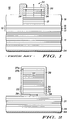
- VCSEL 10 includes a first mirror stack 11 formed of N-type conductivity material, an active region 12 having a first cladding layer 13, an active layer 14 (such as quantum wells and the like) and a second cladding layer 15, and a second mirror stack 17 formed of P-type conductivity material. Second mirror stack 17 is etched, or selectively deposited, to form a mesa-like structure.
- An electrical contact 20 is formed in contact with at least the upper end of second mirror stack 17. Electrical contact 20 defines a window 22 for the emission of light from VCSEL 10 through second mirror stack 17.
- a second electrical contact 24 is positioned over the lower surface of first mirror stack 11. This VCSEL is referred to as having a P-up configuration.
- the top mirror stack is formed of P-type conductivity material.
- the top mirror stack has high resistance because of the reduction in area due to the formation of the mesa-like structure and because it is formed of a material which is already more resistive than if it were formed from N-type conductivity material. Therefore, to reduce series resistance, it has been determined that the portion of the VCSEL having a reduced area, namely the mesa-like structure, should be formed from N-type conductivity material.
- VCSEL 30 vertical cavity surface emitting laser 30 embodying the present invention is illustrated.
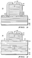
- VCSEL 30 is formed on a substrate 29 in a P-down configuration.
- VCSEL 30 includes a first mirror stack 31 (positioned on substrate 29), formed of a P-type conductivity material, an active region 32 having a first cladding layer 33, an active layer 34 and a second cladding layer 35, and a second mirror stack 37 formed of a N-type conductivity material.
- Second mirror stack 37 is etched, or selectively deposited, to form a mesa-like structure, as described above.
- the series resistance of VCSEL 30 is lowered by increasing the diametric size of second mirror stack 37 which permits spreading of the current flow.
- first mirror stack 31 is formed with P-type conductivity material
- second mirror stack 37 is formed with N-type conductivity material. This further reduces resistance because N-type conductivity material has a lower resistance than does P-type conductivity material.
- the P-down configuration provides the higher resistance P-type conductivity material of first mirror stack 31 with a large area. The large area permits spreading of the current flow, thus reducing resistance.
- the N-type conductivity material of second mirror stack 37 is inherently less resistive, and thus the reduction of the area of second mirror stack 37, formed of N-type conductivity material, to form the mesa will be less significant than if it were conventionally formed of P-type conductivity material.
- Increasing the diametric size of the mesa-like structure and forming second mirror stack 37 of N-type conductivity material greatly reduces resistance, but also allows current flow into active region 32 outside the optical mode. To control the current flow into active region 32, the electrical conductance of a portion 38 of first mirror stack 31 adjacent active region 32 is reduced.
- Portion 38 includes the outer circumference of one or more mirror pairs of first mirror stack 31 adjacent active region 32. This is preferably accomplished by etching second mirror stack 37 to form the mesa like structure, and etching through active layer 32 to first mirror stack 31. Generally, etching active region 32 will cause defects which greatly reduce the lifetime of the VCSEL, or render it completely inoperable. However, due to the increased diametric size of the mesa-like structure, the etched portion of active region 32 is laterally removed from the operative portion of active region 32. The operative portion being within the optical mode or lasing area. Being removed from the optical mode or lasing area, defects generated by the etch will not effect the active region 32 at the optical mode.
- First stack of mirrors 37 is formed predominantly of alternating low and high aluminum containing layers 37a and 37b of AlGaAs distributed Bragg reflectors. Alternating layer 37a and 37b provide alternating high and low indexes of refraction.
- a dielectric layer 39 is deposited and etched back, covering the sides and top of the mesa-like structure and active region 32, leaving the first layer of first mirror stack 31 exposed.
- the first pair of layers or a few pairs of layers of first mirror stack 31 are then etched. This exposes an outer edge of the first pair of layers.
- alternating layers 37a and 37b of low and high aluminum containing AlGaAs adjacent active region 32 are selectively oxidized in accordance with the aluminum content.
- the layer of the mirror pair having a high concentration of aluminum is readily oxidized, reducing its electrical conductance.
- the oxidation in this embodiment is accomplished by subjecting the outer edges of the first mirror layers to a nitrogen ambient containing water moisture. In this ambient the natural oxidation of the aluminum produces high resistance portion 38 within the mirror pairs adjacent active region 32.
- portion 38 of the mirror pairs may be removed by etching. Selective wet etching is performed by using diluted HF or diluted HCL.
- Active region 32 and second mirror stack 37 are protected from the etch or oxidation by dielectric layer 39. Only one or a few mirror pairs adjacent active region 32 is susceptible to the etch or oxidation.
- the optical mode and threshold current can be controlled by the degree of undercut or oxidation without adverse impact on the series resistance.
- portion 38 also helps enhance the reliability and lifetime of VCSEL 10 by allowing the undoped first cladding layer 33 to be fully depleted, reducing migration of both defects and carriers into active layer 34 and causing degradation.
- a lower portion 43 of second mirror stack 37 and active region 32 are etched to provide them with a larger diametric size than the mesa-like structure, to provide room for implants 41.
- a layer of an indium based alloy (e.g. InAlGaP, InAs, etc.), designated 46, can be optionally included in the opening defined by portion 38. All of the operating current flowing in VCSEL 30 flows through the opening defined by portion 38 and, thus, any defects carried by the current must pass through the opening. It has been found that a layer of an indium based alloy substantially prevents defects from passing therethrough.
- this feature produces additional reduction in defects migrating to the active area and, therefore, further increases the life of VCSEL 30.
- portion 38 which is removed or oxidized depends on the overall diametric size of the mesa, and the desired operating mode.
- portion 38 is the diameter of the mirror pairs outside the desired optical mode.
- the reduced electrical conductance of portion 38 results in a funneling of the current into active region 32 at the optical mode. Current travels the shortest distance, path of least resistance, between two points. Therefore, current will pass through active region 32 only in the optical mode as controlled by portion 38.
- the diametric size of the mesa is greater than one times larger than the optical mode of the VCSEL. In the preferred embodiment, the diametric size of the mesa is at least twice as large as the operating mode.
- An electrical contact 40 is formed in contact with at least the upper end of second mirror stack 37. Electrical contact 40 defines a window 42 for the emission of light from VCSEL 30 through second mirror stack 37. A second electrical contact 44 is positioned over the lower surface of first mirror stack 31. The area of electrical contact 40 is increased proportional to the increase in the diametric size of the mesa-like structure. Since window 44 for the emission of light stays the same, corresponding to the optical mode, the larger the diametric size of the mesa-like structure, the larger the area of contact. This gives a much greater area for contact without shadowing the emitting light, thereby reducing series resistance due to ohmic contact.
- N-type conductivity material has less resistance than P-type conductivity material.
Landscapes
- Physics & Mathematics (AREA)
- Condensed Matter Physics & Semiconductors (AREA)
- General Physics & Mathematics (AREA)
- Electromagnetism (AREA)
- Optics & Photonics (AREA)
- Geometry (AREA)
- Semiconductor Lasers (AREA)
Applications Claiming Priority (2)
| Application Number | Priority Date | Filing Date | Title |
|---|---|---|---|
| US55807295A | 1995-11-13 | 1995-11-13 | |
| US558072 | 1995-11-13 |
Publications (1)
| Publication Number | Publication Date |
|---|---|
| EP0773614A1 true EP0773614A1 (fr) | 1997-05-14 |
Family
ID=24228094
Family Applications (1)
| Application Number | Title | Priority Date | Filing Date |
|---|---|---|---|
| EP96118024A Withdrawn EP0773614A1 (fr) | 1995-11-13 | 1996-11-11 | VCSEL à nervure à faille résistance du type p en bas et méthode de fabrication |
Country Status (2)
| Country | Link |
|---|---|
| EP (1) | EP0773614A1 (fr) |
| KR (1) | KR970031126A (fr) |
Cited By (11)
| Publication number | Priority date | Publication date | Assignee | Title |
|---|---|---|---|---|
| EP0926786A3 (fr) * | 1997-12-23 | 2000-04-26 | Lucent Technologies Inc. | Laser à émission de surface à cavité verticale avec guides optiques et guides de courant separés |
| EP0981168A3 (fr) * | 1998-08-18 | 2000-07-19 | TRW Inc. | Composants semiconducteurs microoptiques et méthode de fabrication |
| GB2399940A (en) * | 2003-03-25 | 2004-09-29 | Sharp Kk | Vertical cavity surface emitting laser |
| JP2017204579A (ja) * | 2016-05-12 | 2017-11-16 | スタンレー電気株式会社 | 垂直共振器型発光素子及び垂直共振器型発光素子の製造方法 |
| US20180287345A1 (en) * | 2017-04-04 | 2018-10-04 | Apple Inc. | VCSELs with improved optical and electrical confinement |
| US10707650B2 (en) | 2016-03-04 | 2020-07-07 | Princeton Optronics, Inc. | High-speed VCSEL device |
| US10825952B2 (en) | 2017-01-16 | 2020-11-03 | Apple Inc. | Combining light-emitting elements of differing divergence on the same substrate |
| US11322910B2 (en) | 2019-02-21 | 2022-05-03 | Apple Inc. | Indium-phosphide VCSEL with dielectric DBR |
| US11374381B1 (en) | 2019-06-10 | 2022-06-28 | Apple Inc. | Integrated laser module |
| US11418010B2 (en) | 2019-04-01 | 2022-08-16 | Apple Inc. | VCSEL array with tight pitch and high efficiency |
| US12494618B2 (en) | 2022-09-14 | 2025-12-09 | Apple Inc. | Vertical emitters with integrated final-stage transistor switch |
Citations (1)
| Publication number | Priority date | Publication date | Assignee | Title |
|---|---|---|---|---|
| US5256596A (en) * | 1992-03-26 | 1993-10-26 | Motorola, Inc. | Top emitting VCSEL with implant |
-
1996
- 1996-11-08 KR KR1019960053577A patent/KR970031126A/ko not_active Withdrawn
- 1996-11-11 EP EP96118024A patent/EP0773614A1/fr not_active Withdrawn
Patent Citations (1)
| Publication number | Priority date | Publication date | Assignee | Title |
|---|---|---|---|---|
| US5256596A (en) * | 1992-03-26 | 1993-10-26 | Motorola, Inc. | Top emitting VCSEL with implant |
Non-Patent Citations (2)
| Title |
|---|
| CHOQUETTE K D ET AL: "CAVITY CHARACTERISTICS OF SELECTIVELY OXIDIZED VERTICAL-CAVITY LASERS", APPLIED PHYSICS LETTERS, vol. 66, no. 25, 19 June 1995 (1995-06-19), pages 3413 - 3415, XP000520299 * |
| WILSON G C ET AL: "HIGH SINGLE-MODE OUTPUT POWER FROM COMPACT EXTERNAL MICROCAVITY SURFACE-EMITTING LASER DIODE", APPLIED PHYSICS LETTERS, vol. 63, no. 24, 13 December 1993 (1993-12-13), pages 3265 - 3267, XP000416519 * |
Cited By (12)
| Publication number | Priority date | Publication date | Assignee | Title |
|---|---|---|---|---|
| EP0926786A3 (fr) * | 1997-12-23 | 2000-04-26 | Lucent Technologies Inc. | Laser à émission de surface à cavité verticale avec guides optiques et guides de courant separés |
| EP0981168A3 (fr) * | 1998-08-18 | 2000-07-19 | TRW Inc. | Composants semiconducteurs microoptiques et méthode de fabrication |
| GB2399940A (en) * | 2003-03-25 | 2004-09-29 | Sharp Kk | Vertical cavity surface emitting laser |
| US10707650B2 (en) | 2016-03-04 | 2020-07-07 | Princeton Optronics, Inc. | High-speed VCSEL device |
| JP2017204579A (ja) * | 2016-05-12 | 2017-11-16 | スタンレー電気株式会社 | 垂直共振器型発光素子及び垂直共振器型発光素子の製造方法 |
| US10825952B2 (en) | 2017-01-16 | 2020-11-03 | Apple Inc. | Combining light-emitting elements of differing divergence on the same substrate |
| US20180287345A1 (en) * | 2017-04-04 | 2018-10-04 | Apple Inc. | VCSELs with improved optical and electrical confinement |
| US11381060B2 (en) * | 2017-04-04 | 2022-07-05 | Apple Inc. | VCSELs with improved optical and electrical confinement |
| US11322910B2 (en) | 2019-02-21 | 2022-05-03 | Apple Inc. | Indium-phosphide VCSEL with dielectric DBR |
| US11418010B2 (en) | 2019-04-01 | 2022-08-16 | Apple Inc. | VCSEL array with tight pitch and high efficiency |
| US11374381B1 (en) | 2019-06-10 | 2022-06-28 | Apple Inc. | Integrated laser module |
| US12494618B2 (en) | 2022-09-14 | 2025-12-09 | Apple Inc. | Vertical emitters with integrated final-stage transistor switch |
Also Published As
| Publication number | Publication date |
|---|---|
| KR970031126A (ko) | 1997-06-26 |
Similar Documents
| Publication | Publication Date | Title |
|---|---|---|
| US5359618A (en) | High efficiency VCSEL and method of fabrication | |
| EP1306943B1 (fr) | Laser à couche de confinement du courant à variation sélective | |
| EP0926786B1 (fr) | Laser à émission de surface à cavité verticale avec guides optiques et guides de courant separés | |
| US6936486B2 (en) | Low voltage multi-junction vertical cavity surface emitting laser | |
| EP1073171B1 (fr) | Laser à émission de surface à cavité verticale avec injection latérale | |
| US6570905B1 (en) | Vertical cavity surface emitting laser with reduced parasitic capacitance | |
| US6914925B2 (en) | Vertical cavity surface emitting semiconductor laser device | |
| KR20050053763A (ko) | 광전자장치용 분산 브래그 반사기 | |
| EP0773614A1 (fr) | VCSEL à nervure à faille résistance du type p en bas et méthode de fabrication | |
| JP3116088B2 (ja) | 面発光レーザ装置 | |
| US5748661A (en) | Integrated lateral detector and laser device and method of fabrication | |
| JPWO2006100975A1 (ja) | トンネル接合発光素子 | |
| EP0501246B1 (fr) | Dispositif interrupteur optoélectronique | |
| EP0772266A1 (fr) | VCSEL à nervure à faible résistance et méthode de fabrication | |
| JP2618610B2 (ja) | 垂直共振器型面発光半導体レーザ | |
| JPH05283796A (ja) | 面発光型半導体レーザ | |
| US5394421A (en) | Semiconductor laser device including a step electrode in a form of eaves | |
| JP2001332812A (ja) | 面発光半導体レーザ素子 | |
| US7579200B2 (en) | Semiconductor light emitting apparatus and method of fabricating the same | |
| EP0791990A1 (fr) | VCSEL à nervure à faible résistance du type p en bas et méthode de fabrication | |
| US5567646A (en) | Method of making a stripe-geometry II/VI semiconductor gain-guided injection laser structure using ion implantation | |
| JP3685541B2 (ja) | 半導体レーザ装置およびその製造方法 | |
| WO2004047242A1 (fr) | Laser a emission par la surface a cavite verticale a multi-jonctions de basse tension | |
| JP3336981B2 (ja) | 半導体積層構造 | |
| JPH1126865A (ja) | 半導体レーザ |
Legal Events
| Date | Code | Title | Description |
|---|---|---|---|
| PUAI | Public reference made under article 153(3) epc to a published international application that has entered the european phase |
Free format text: ORIGINAL CODE: 0009012 |
|
| AK | Designated contracting states |
Kind code of ref document: A1 Designated state(s): DE FR GB |
|
| STAA | Information on the status of an ep patent application or granted ep patent |
Free format text: STATUS: THE APPLICATION IS DEEMED TO BE WITHDRAWN |
|
| 18D | Application deemed to be withdrawn |
Effective date: 19971117 |
|
| RIN1 | Information on inventor provided before grant (corrected) |
Inventor name: CLAISSE, PAUL Inventor name: SHEIH, CHAN-LONG Inventor name: LEBBY, MICHAEL S. |