EP0774787A2 - Anordnung von organischen Vollfarbenleuchtdioden - Google Patents
Anordnung von organischen Vollfarbenleuchtdioden Download PDFInfo
- Publication number
- EP0774787A2 EP0774787A2 EP96117868A EP96117868A EP0774787A2 EP 0774787 A2 EP0774787 A2 EP 0774787A2 EP 96117868 A EP96117868 A EP 96117868A EP 96117868 A EP96117868 A EP 96117868A EP 0774787 A2 EP0774787 A2 EP 0774787A2
- Authority
- EP
- European Patent Office
- Prior art keywords
- layer
- full color
- light emitting
- substrate
- emitting diode
- Prior art date
- Legal status (The legal status is an assumption and is not a legal conclusion. Google has not performed a legal analysis and makes no representation as to the accuracy of the status listed.)
- Granted
Links
- 239000000758 substrate Substances 0.000 claims abstract description 41
- 239000004020 conductor Substances 0.000 claims abstract description 14
- 239000004065 semiconductor Substances 0.000 claims abstract description 14
- 239000003989 dielectric material Substances 0.000 claims abstract description 9
- 239000000463 material Substances 0.000 claims description 39
- 238000004519 manufacturing process Methods 0.000 claims description 17
- 229910052751 metal Inorganic materials 0.000 claims description 16
- 239000002184 metal Substances 0.000 claims description 16
- 229920002120 photoresistant polymer Polymers 0.000 claims description 12
- 238000000151 deposition Methods 0.000 claims description 11
- VYPSYNLAJGMNEJ-UHFFFAOYSA-N Silicium dioxide Chemical compound O=[Si]=O VYPSYNLAJGMNEJ-UHFFFAOYSA-N 0.000 claims description 10
- 238000005530 etching Methods 0.000 claims description 8
- 238000000059 patterning Methods 0.000 claims description 8
- 229910052581 Si3N4 Inorganic materials 0.000 claims description 5
- 239000000377 silicon dioxide Substances 0.000 claims description 5
- HQVNEWCFYHHQES-UHFFFAOYSA-N silicon nitride Chemical compound N12[Si]34N5[Si]62N3[Si]51N64 HQVNEWCFYHHQES-UHFFFAOYSA-N 0.000 claims description 5
- 229910010272 inorganic material Inorganic materials 0.000 claims description 3
- 239000011147 inorganic material Substances 0.000 claims description 3
- 229920000620 organic polymer Polymers 0.000 claims description 3
- PNEYBMLMFCGWSK-UHFFFAOYSA-N aluminium oxide Inorganic materials [O-2].[O-2].[O-2].[Al+3].[Al+3] PNEYBMLMFCGWSK-UHFFFAOYSA-N 0.000 claims description 2
- 238000007789 sealing Methods 0.000 claims description 2
- 235000012239 silicon dioxide Nutrition 0.000 claims description 2
- 238000000034 method Methods 0.000 description 28
- 230000008569 process Effects 0.000 description 13
- 238000005516 engineering process Methods 0.000 description 7
- 230000006870 function Effects 0.000 description 6
- 239000011295 pitch Substances 0.000 description 5
- 238000010276 construction Methods 0.000 description 4
- 230000008021 deposition Effects 0.000 description 4
- 238000001312 dry etching Methods 0.000 description 4
- 150000002739 metals Chemical class 0.000 description 4
- 238000000623 plasma-assisted chemical vapour deposition Methods 0.000 description 4
- 238000005266 casting Methods 0.000 description 3
- 229910052681 coesite Inorganic materials 0.000 description 3
- 239000003086 colorant Substances 0.000 description 3
- 229910052906 cristobalite Inorganic materials 0.000 description 3
- 239000002019 doping agent Substances 0.000 description 3
- 238000001704 evaporation Methods 0.000 description 3
- 230000008020 evaporation Effects 0.000 description 3
- 238000012986 modification Methods 0.000 description 3
- 230000004048 modification Effects 0.000 description 3
- 230000008447 perception Effects 0.000 description 3
- 229920005548 perfluoropolymer Polymers 0.000 description 3
- 229910052682 stishovite Inorganic materials 0.000 description 3
- 229910052905 tridymite Inorganic materials 0.000 description 3
- 238000003491 array Methods 0.000 description 2
- QVGXLLKOCUKJST-UHFFFAOYSA-N atomic oxygen Chemical compound [O] QVGXLLKOCUKJST-UHFFFAOYSA-N 0.000 description 2
- 230000015572 biosynthetic process Effects 0.000 description 2
- 239000010406 cathode material Substances 0.000 description 2
- 239000011159 matrix material Substances 0.000 description 2
- 239000011368 organic material Substances 0.000 description 2
- 229910052760 oxygen Inorganic materials 0.000 description 2
- 239000001301 oxygen Substances 0.000 description 2
- 229920000767 polyaniline Polymers 0.000 description 2
- 238000012800 visualization Methods 0.000 description 2
- 238000001039 wet etching Methods 0.000 description 2
- OYPRJOBELJOOCE-UHFFFAOYSA-N Calcium Chemical compound [Ca] OYPRJOBELJOOCE-UHFFFAOYSA-N 0.000 description 1
- RYGMFSIKBFXOCR-UHFFFAOYSA-N Copper Chemical compound [Cu] RYGMFSIKBFXOCR-UHFFFAOYSA-N 0.000 description 1
- WHXSMMKQMYFTQS-UHFFFAOYSA-N Lithium Chemical compound [Li] WHXSMMKQMYFTQS-UHFFFAOYSA-N 0.000 description 1
- FYYHWMGAXLPEAU-UHFFFAOYSA-N Magnesium Chemical compound [Mg] FYYHWMGAXLPEAU-UHFFFAOYSA-N 0.000 description 1
- BQCADISMDOOEFD-UHFFFAOYSA-N Silver Chemical compound [Ag] BQCADISMDOOEFD-UHFFFAOYSA-N 0.000 description 1
- 239000002253 acid Substances 0.000 description 1
- 230000002378 acidificating effect Effects 0.000 description 1
- 229910052782 aluminium Inorganic materials 0.000 description 1
- XAGFODPZIPBFFR-UHFFFAOYSA-N aluminium Chemical compound [Al] XAGFODPZIPBFFR-UHFFFAOYSA-N 0.000 description 1
- 230000004888 barrier function Effects 0.000 description 1
- 229910052791 calcium Inorganic materials 0.000 description 1
- 239000011575 calcium Substances 0.000 description 1
- 230000015556 catabolic process Effects 0.000 description 1
- 239000011248 coating agent Substances 0.000 description 1
- 238000000576 coating method Methods 0.000 description 1
- 229910052802 copper Inorganic materials 0.000 description 1
- 239000010949 copper Substances 0.000 description 1
- 238000006731 degradation reaction Methods 0.000 description 1
- 230000001419 dependent effect Effects 0.000 description 1
- 238000001514 detection method Methods 0.000 description 1
- 238000003618 dip coating Methods 0.000 description 1
- 230000002349 favourable effect Effects 0.000 description 1
- 239000007850 fluorescent dye Substances 0.000 description 1
- PCHJSUWPFVWCPO-UHFFFAOYSA-N gold Chemical compound [Au] PCHJSUWPFVWCPO-UHFFFAOYSA-N 0.000 description 1
- 229910052737 gold Inorganic materials 0.000 description 1
- 239000010931 gold Substances 0.000 description 1
- 238000010438 heat treatment Methods 0.000 description 1
- 229910052738 indium Inorganic materials 0.000 description 1
- APFVFJFRJDLVQX-UHFFFAOYSA-N indium atom Chemical compound [In] APFVFJFRJDLVQX-UHFFFAOYSA-N 0.000 description 1
- AMGQUBHHOARCQH-UHFFFAOYSA-N indium;oxotin Chemical compound [In].[Sn]=O AMGQUBHHOARCQH-UHFFFAOYSA-N 0.000 description 1
- 239000007788 liquid Substances 0.000 description 1
- 239000004973 liquid crystal related substance Substances 0.000 description 1
- 229910052744 lithium Inorganic materials 0.000 description 1
- 238000001459 lithography Methods 0.000 description 1
- 229910052749 magnesium Inorganic materials 0.000 description 1
- 239000011777 magnesium Substances 0.000 description 1
- 239000000203 mixture Substances 0.000 description 1
- 125000002524 organometallic group Chemical group 0.000 description 1
- 229920000642 polymer Polymers 0.000 description 1
- 239000002861 polymer material Substances 0.000 description 1
- 229910052709 silver Inorganic materials 0.000 description 1
- 239000004332 silver Substances 0.000 description 1
- 238000004528 spin coating Methods 0.000 description 1
- 238000004544 sputter deposition Methods 0.000 description 1
- 238000010345 tape casting Methods 0.000 description 1
- 238000002207 thermal evaporation Methods 0.000 description 1
- 239000010409 thin film Substances 0.000 description 1
- 238000007738 vacuum evaporation Methods 0.000 description 1
Images

Classifications
-
- H—ELECTRICITY
- H10—SEMICONDUCTOR DEVICES; ELECTRIC SOLID-STATE DEVICES NOT OTHERWISE PROVIDED FOR
- H10K—ORGANIC ELECTRIC SOLID-STATE DEVICES
- H10K59/00—Integrated devices, or assemblies of multiple devices, comprising at least one organic light-emitting element covered by group H10K50/00
- H10K59/10—OLED displays
- H10K59/17—Passive-matrix OLED displays
-
- H—ELECTRICITY
- H10—SEMICONDUCTOR DEVICES; ELECTRIC SOLID-STATE DEVICES NOT OTHERWISE PROVIDED FOR
- H10K—ORGANIC ELECTRIC SOLID-STATE DEVICES
- H10K59/00—Integrated devices, or assemblies of multiple devices, comprising at least one organic light-emitting element covered by group H10K50/00
- H10K59/30—Devices specially adapted for multicolour light emission
- H10K59/35—Devices specially adapted for multicolour light emission comprising red-green-blue [RGB] subpixels
Definitions
- the present invention relates to organic light emitting diode image manifestation apparatus and to a novel method of fabrication of a full color organic light emitting diode (LED) array for image manifestation apparatus.
- LED organic light emitting diode
- An organic LED array for image display applications is composed of a plurality of organic light emitting pixels arranged in rows and columns.
- a full color array can be achieved by constructing three sub-pixels in one pixel, each sub-pixel emitting red, green or blue. This technology is generally utilized in cathode-ray-tube color displays.
- An alternative full color array makes use of a white emitter as a backlight in conjunction with a color filter array containing pixels patterned into red, green, and blue sub-pixels.
- the second technology to generate full color has been widely used in full color liquid crystal displays.
- the color filter based technology is generally considered less favorable due to the luminescent efficiency limits of most organic LED devices.
- each individual organic light emitting pixel is divided into red, green and blue sub-pixels.
- Each sub-pixel is generally constructed with a light transmissive first electrode, an organic electroluminescent medium deposited on the first electrode, and a metallic electrode on top of the organic electroluminescent medium. The color of the sub-pixel is determined by the electroluminescent medium employed.
- the electrodes connect the pixels to form a two-dimensional X-Y addressing pattern.
- the X-Y addressing pattern is achieved by patterning the light transmissive electrodes in the X direction and patterning the metallic electrodes in the Y direction, with X and Y directions being perpendicular to each other.
- the patterning of the electrodes is usually accomplished by either shadow mask or etching techniques. Due to the technical limits of shadow masks, only etching processes are being utilized for image displays, which have generally sub-pixel pitches less then 0.2 mm.
- the etching technique can be divided into two categories: wet and dry. While wet etching is performed in an acidic liquid medium, dry etching is usually carried out in a plasma atmosphere.
- Scozzafava in EP 349,265 disclosed an organic electroluminescent image display device and a process for its fabrication based on a wet etching technology.
- the metallic electrodes used for cathode contacts in organic LEDs usually contain a stable metal and a highly reactive metal (with work function less then 4 eV) that can not survive in the acid etching processes.
- the dry etching processes for metallic electrodes in an organic LED array is also problematic.
- the high temperature (> 200°C) and reactive ion atmosphere required in dry etching process may affect the integrity of the organic materials as well as the active metal contained in the metallic electrodes in an organic LED array.
- Tang in U.S. Patent Number 5,276,380 discloses a shadow wall method to fabricate the two-dimensional array without the need of the etching of the metallic electrodes.
- the shadow wall method includes: patterning the transparent electrode first; building dielectric walls that are orthogonal to the transparent electrodes, capable of shadowing an adjacent pixel area, and with a height exceeding the thickness of the organic medium; depositing organic electroluminescent medium; and depositing the cathode metals from an angle of 15° to 45° with respect to the deposition surface. Since the height of the dielectric walls exceeds the thickness of the organic medium, isolated parallel metal stripes are formed. Thus, a X-Y addressable array is achieved without the need of metal etching. Though this method seems to be viable for metal patterning, it is limited to certain pitch dimensions, and potentially could introduce leakage in pixels in the array.
- a novel method of fabricating a full color diode array on a light transmissive substrate is disclosed in a copending U.S. Patent Application entitled “Full Color Organic Light Emitting Diode Array", bearing serial number 08/409,129, filed March 22, 1995.
- diode arrays on semiconductor substrates so that drivers and the like can be integrated directly with the array. Since the semiconductor substrates generally are not transparent to the emitted light, some important modifications must be made in the array and in the fabrication process.
- a full color organic light emitting diode array including a semiconductor substrate having a planar surface.
- a plurality of laterally spaced, electrically conductive strips are arranged in rows on the surface of the substrate with portions of the surface of the substrate exposed therebetween and a layer of dielectric medium is deposited over the conductive strips and the portions of the surface of the substrate.
- the dielectric medium is etched to define a plurality of cavity structures, with each cavity structure defining a sub-pixel, and the plurality of cavity structures being positioned in rows in overlying relationship to the plurality of conductive strips with individual cavity structures positioned in overlying relationship to an associated conductive strip so as to expose a portion of the conductive strip.
- Three electroluminescent media each including at least a layer of active emitter material and a layer of a light transmissive, electrically conductive material are laterally and alternatively deposited in the cavity structures on the exposed associated conductive strip, with all of the cavity structures in each individual row containing only one kind of the three electroluminescent media.
- a transparent dielectric material is positioned in sealing engagement over the cavity structures and the electrically conductive material is connected in columns orthogonal to the conductive strips to complete the array.
- Methods of fabrication of a full color organic light emitting diode array are also disclosed wherein some of the above steps are repeated to form two or three groups of sub-pixels.
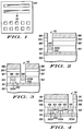
- FIG. 1 a plan view of trenches 10 and wells 20 are intentionally depicted on the same substrate to illustrate their dimensional difference.
- Both the trench and the well structures are generally formed by photolithographically patterning a dielectric layer 103 that has been deposited on top of electrically conductive strips 101 (see FIG. 2), of a convenient metal or the like, that are in turn supported by an underlying semiconductor substrate 100, as will be described presently.
- Each trench 10 is defined as a long, narrow, straight, deep depression with four relative steep (substantially vertical) sides formed in dielectric layer 103.
- Each trench 10 typically takes the shape of a rectangular parallelepiped as shown in FIG. 1.
- a trench 10 generally extends across substrate 100 in a direction either perpendicular to underlying electrically conductive strips 101 (see FIG. 6 for example) or parallel to and on the top of underlying electrically conductive strips 101.
- trenches 10 are preferably perpendicular to underlying electrically strips 101 so as to form a x-y addressable matrix.
- a plurality of pixels can be constructed in each single trench 10.
- Each well 20 is defined as a hole formed in dielectric layer 103 with a rectangular, square or circular shape of opening, and steep (substantially vertical) side walls. Wells 20 are characterized by the small feature size and nearly isotropic shape of opening. A plurality of wells 20 are constructed in a row across substrate 100 in overlying relationship to electrically conductive strips 101 (see FIG. 6 for example). Each well 20 defines the shape of a sub-pixel in the array. Either trenches 10 or wells 20 can be used in fabrication of a full color organic LED array for image display, as will be described presently. For convenience of further disclosure, both trenches 10 and wells 20 are hereinafter referred to in general as cavity structures, which term also includes other variations on these structures.
- the LED array to be described is characterized in that the array is capable of full color image display.
- Each pixel is composed of three sub-pixels, each having a specific electroluminescent medium capable of emitting light of a different hue, preferably red, or green, or blue.
- Each sub-pixel is constructed with a cavity structure having electrically conductive strips 101 at the bottom, dielectric medium on the side walls and a transparent dielectric material on the top.
- FIGS. 2, 3 , 4 and 5 are cross sectional views illustrating a single pixel with three sub-pixels of the LED array at successive stages of fabrication.
- a relative flat, semiconductor substrate 100 which may be, for example, a typical CMOS substrate (to be explained in more detail presently).
- CMOS substrate is preferred because of the low power driver components which can be incorporated.
- the driver circuits and other integrated circuits will be formed before the organic LED array and any high steps or the like which develop on the substrate can be overcome by traditional planarization.
- a layer of electrically conductive material is deposited on the upper surface of substrate 100, which layer is selected from a variety of stable metals, organic or inorganic conductors, such as aluminum, silver, copper or gold.
- the layer is then patterned by conventional lithographic techniques to form a plurality of parallel conductive strips 101 that are capable of being addressed in a row fashion (or, conversely, a column fashion if desired) and will serve as an anode or cathode electrode (a cathode in this specific embodiment) in the final array.
- a layer of dielectric medium 103 is deposited on top of conductive strips 101 and exposed portions of substrate 100, by techniques such as thermal evaporation, sputtering or plasma enhanced chemical vapor deposition.
- Dielectric medium 103 used in the construction of cavity structures can be an organic polymer or inorganic materials. It is preferred to use an inorganic dielectric material such as silicon dioxide, silicon nitride, or alumina, which is usually a better barrier to oxygen and moisture than organic polymer materials.
- the thickness of dielectric medium 103 determines the depth of the cavity structures and may vary from 10 ⁇ m to 0.1 ⁇ m. For easy processing, a thickness of less then 1 ⁇ m is preferred.
- a layer 105 of photoresist is spin-coated on top of dielectric medium 103 and patterned with a light source through a mask (not shown). Though both positive and negative resist can be used, it is preferred to use a positive resist for its high resolution and excellent dry etching resistance. After a heat treatment, layer 105 of photoresist is developed to expose underlying dielectric medium 103. Dielectric medium 103 is then patterned by conventional wet or dry etch technique to form a cavity structure or structures 112. Dry etch is generally preferred for its anisotropic character that renders relatively straight or substantially vertical side walls.
- metals with a work function less than 4.0 eV e.g. lithium, magnesium, indium, calcium etc.
- metals with work function greater than 4.0 eV may also be employed as the cathode material to yield an efficient LED display as the electron injecting and transporting abilities of the materials used in the electroluminescent media improve.
- Electroluminescent medium 202 is deposited inside cavity structure 112, and in overlying relationship to a single conductive strip of the plurality of conductive strips 101.
- Electroluminescent medium 202 generally consists of (for purposes of example only) a layer of electron transporting material, a layer of active emitter material capable of emitting the first hue, and a layer of hole transporting material. Since various individual and combinations of layers of electroluminescent material 202 are known, each individual layer is not described in detail herein.
- a layer 202A of a transparent conductive material, such as conductive polyaniline (PANI), or indium-tin-oxide (ITO) is deposited inside cavity structure 112 as a second electrode (e.g., the anode).
- Layer 202A can be positioned or deposited in cavity structure 112 by any convenient process, such as evaporation or casting, without damaging electroluminescent material 202.
- layer 202A may be considered a portion of electroluminescent material 202.
- cavity structure 112 is then sealed by deposition of a thick layer 106 of a transparent dielectric material, such as SiO 2 , silicon nitride deposited by low temperature PECVD, or a transparent perfluoro polymer (e.g. Teflon-AF), as a cap for cavity structure 112.
- a transparent dielectric material such as SiO 2 , silicon nitride deposited by low temperature PECVD, or a transparent perfluoro polymer (e.g. Teflon-AF)
- the thickness of layer 106 is controlled so that cavity structure 112 is just filled to the height of dielectric medium 103.
- a lift-off of photoresist layer 105 is performed to complete the first sub-pixel capable of emitting a first hue, red in this specific embodiment, in the pixel.
- electroluminescent medium 203 is deposited in cavity structure 113 and in overlying relationship to the single conductive strip of the plurality of conductive strips 101.
- electroluminescent medium 203 generally consists of a layer of electron transporting material, a layer of active emitter material capable of emitting a second hue, and a layer of hole transporting material.
- a layer 203A of a transparent conductive material is then deposited as a second electrode (e.g. the cathode).
- Layer 203A can be positioned or deposited in cavity structure 113 by any convenient process, such as evaporation or casting, without damaging electroluminescent material 203.
- layer 203A may be considered a portion of electroluminescent material 203.
- cavity structure 113 is then sealed by deposition of a thick layer 108 of a transparent dielectric material, such as SiO 2 , silicon nitride deposited by low temperature PECVD, or a transparent perfluoro polymer (e.g. Teflon-AF), as a cap for cavity structure 113.
- a transparent dielectric material such as SiO 2 , silicon nitride deposited by low temperature PECVD, or a transparent perfluoro polymer (e.g. Teflon-AF)
- the thickness of layer 108 is controlled so that cavity structure 113 is just filled to the height of dielectric medium 103.
- a lift-off of photoresist layer 107 is performed to complete the construction of the second sub-pixel in the pixel, capable of emitting the second hue, in this specific embodiment green, is complete.
- a layer 109 of photoresist is spin-coated on top of the first and second sub-pixels and dielectric medium 103 and patterned and developed, generally as described above.
- the exposed dielectric medium 103 is then patterned to form a third cavity structure or structures 114 adjacent to the first and second sub-pixels.
- An electroluminescent medium 204 is deposited in cavity structure 114 and in overlying relationship to the single conductive strip of the plurality of conductive strips 101.
- electroluminescent medium 204 generally consists of a layer of electron transporting material, a layer of active emitter material capable of emitting a third hue, and a layer of hole transporting material.
- a layer 204A of a transparent conductive material is then deposited as a second electrode (e.g. the cathode).
- Layer 204A can be positioned or deposited in cavity structure 114 by any convenient process, such as evaporation or casting, without damaging electroluminescent material 204.
- layer 204A may be considered a portion of electroluminescent material 204.
- cavity structure 114 is then sealed by deposition of a thick layer 110 of a transparent dielectric material, such as SiO 2 , silicon nitride deposited by low temperature PECVD, or a transparent perfluoro polymer (e.g. Teflon-AF), as a cap for cavity structure 114.
- a transparent dielectric material such as SiO 2 , silicon nitride deposited by low temperature PECVD, or a transparent perfluoro polymer (e.g. Teflon-AF)
- the thickness of layer 110 is controlled so that cavity structure 114 is just filled to the height of dielectric medium 103.
- a lift-off of photoresist layer 109 is performed to complete the construction of the third sub-pixel in the pixel, capable of emitting the third hue, in this specific embodiment blue, is complete.
- the complete pixel capable of emitting three primary colors is illustrated in FIG. 5.
- the sub-pixels are then connected, generally by metal strips (not shown) contacting transparent conductive strips 202A, 203A, and 204A adjacent the ends of the columns.
- the metal strips can be formed by either lithographically patterning a blanket layer of deposited metal or depositing of metal over a resist-masked pattern followed by a lift-off process.
- FIG. 6 is a plan view of an organic LED array with portions broken away to illustrate three different stages of the fabrication. Proceeding from left to right in FIG. 6, an area 121 illustrates the LED array at a stage where patterned electrically conductive strips 101 have been formed on semiconductor substrate 100. A central area 122 in FIG. 6 illustrates the stage where individual sub-pixels of electroluminescent media 202, 203, and 204 capable of emitting three hues, in this embodiment the primary colors red, green and blue, have been deposited in cavity structures 112, 113 and 114, respectively. Although the sub-pixels are illustrated as individual squares (wells) it will be understood that entire cavity structures could contain electroluminescent material and only the electroluminescent material between electrodes 101 and 202A, 203A, or 204A would be activated.
- An area 123 illustrates the array after transparent conductive strips 202A, 203A, and 204A have been deposited in cavity structures 112, 113, and 114.
- transparent conductive strips 202A, 203A, and 204A extend the length of cavity structures 112, 113, and 114 to an edge of substrate 100 for conveniently connecting the sub-pixels of all pixels in columns (or rows) as anodic electrodes. It will of course be understood by those skilled in the art that transparent conductive strips 202A, 203A, and 204A can be connected into columns or rows utilizing many other processes, but the process described is generally the most convenient and retains the seal of the various cavity structures.
- FIG. 7 a simplified view in top plan of a complete LED array in accordance with the present invention is illustrated.
- the ends of conductive strips 101 are illustrated connected to row drivers 225, which are formed in substrate 100 as CMOS drivers.
- External connection pads 226 are positioned at the edge of substrate 100 for connection to further external circuitry.
- the ends of transparent conductive strips 202A, 203A, and 204A are illustrated connected to column drivers 230, which are formed in substrate 100 as CMOS drivers.
- External connection pads 231 are positioned at the edge of substrate 100 for connection to further external circuitry.
- Specific details of drivers 225 and 230 are not illustrated since a large variety of specific driver circuits could be utilized, depending upon the specific type of driving, addressing, etc. utilized.
- cavity structures 112, 113 and 114 have been depicted as trenches, it should be understood that an array of well structures can be fabricated in similar fashion, with the exception that the orientation of the trench structures is, preferably, perpendicular to and across all conductive strips 101 in order to form the x-y addressable matrix illustrated in FIG. 7.
- the number of pixels and the sub-pixel pitch that is the width of a cavity structure, in an array, needed for an image display application, are dependent upon the resolution and size of the display required for the specific application. For example, a minimum of 640 x 480 pixels, each having three sub-pixels and with a sub-pixel pitch less than 0.1 mm, are needed for satisfactory resolution in a 13 inch diagonal color VGA type of display.
- the pixel pitch is confined only by the limit of lithography technology, which is around 0.5 ⁇ m in current manufacturing technology.
- the array disclosed in this embodiment has inherently superior stability over any of the arrays disclosed in the prior art.
- the organic electroluminescent medium in each sub-pixel (well structure) or row of sub-pixels (trench structure) are enclosed in a well or trench by a first electrode at the bottom, a dielectric medium on the side and a transparent dielectric cap on the top.
- the disclosed cavity structures significantly reduce the ambient (oxygen and moisture) degradation of the display elements.
- the materials used as the electroluminescent medium in the array disclosed in this invention can take any of the forms of organic EL devices disclosed in the prior art.
- the electroluminescent medium generally consists of a layer of electron transporting material, a layer of active emitter, and a layer of hole transporting material.
- Organic, organometallic, polymeric or any combination of those materials can be used as hole transporting materials, active emitters and electron transporting materials. It will of course be understood that in some special applications either or both of the hole transporting material and the electron transporting material may be eliminated, although this will generally result in poor light emission.
- three different active emitters that would generate the desired color emissions in a pixel can be utilized.
- a fluorescent dopant used for enhancement of the emission efficiency for each individual color in a sub-pixel can also be incorporated.
- a single emitter capable of blue emission is used as host emitters in all three sub-pixels.
- three sub-pixels are then doped with three guest dopants of efficient fluorescent dyes capable of red, green and blue emissions, respectively.
- the guest dopants act as the real emitters while the host emitter serves as an excited energy transporting medium.
- the organic electroluminescent media are deposited by vacuum evaporation when sublimable materials are used. They can also be deposited by other techniques such as injection-fill, spin-coating, roll-coating, dip-coating or doctor-blading from a suitable solution when a polymeric material is used. A mixture of the above-mentioned techniques may be needed in cases where a heterostructure array composed of both sublimable materials and polymers is to be built.
- a pattern of light emission from the LED array can be seen from the top surface of the LED array.
- the LED array is driven to emit light by programming electronic drivers 225 and 230, which sequentially addresses one row of sub-pixels at a time and repeats the addressing sequence at such a rate that the interval between repeated addressing of the same row is less than the detection limit of the human eye, typically less than 1/60th of a second.
- the eye sees an image formed by the light emission from all of the addressed rows, though the device at any moment is emitting from only one row.
- Colors for an image are generated by addressing a combination of sub-pixels in each pixel, generally as follows:
- an organic LED array capable of full color are also applicable to the fabrication of an array for either a monochrome or a multicolor (other than full color) image.
- an array for a monochrome or a multicolor image display application can be fabricated by the same methods disclosed in the foregoing.
Landscapes
- Electroluminescent Light Sources (AREA)
- Devices For Indicating Variable Information By Combining Individual Elements (AREA)
- Led Devices (AREA)
Applications Claiming Priority (2)
| Application Number | Priority Date | Filing Date | Title |
|---|---|---|---|
| US560457 | 1995-11-17 | ||
| US08/560,457 US5736754A (en) | 1995-11-17 | 1995-11-17 | Full color organic light emitting diode array |
Publications (3)
| Publication Number | Publication Date |
|---|---|
| EP0774787A2 true EP0774787A2 (de) | 1997-05-21 |
| EP0774787A3 EP0774787A3 (de) | 1998-05-13 |
| EP0774787B1 EP0774787B1 (de) | 2004-02-25 |
Family
ID=24237903
Family Applications (1)
| Application Number | Title | Priority Date | Filing Date |
|---|---|---|---|
| EP96117868A Expired - Lifetime EP0774787B1 (de) | 1995-11-17 | 1996-11-07 | Anordnung von organischen Vollfarbenleuchtdioden |
Country Status (5)
| Country | Link |
|---|---|
| US (1) | US5736754A (de) |
| EP (1) | EP0774787B1 (de) |
| KR (1) | KR100430699B1 (de) |
| DE (1) | DE69631635T2 (de) |
| TW (1) | TW318966B (de) |
Cited By (8)
| Publication number | Priority date | Publication date | Assignee | Title |
|---|---|---|---|---|
| WO2000011728A1 (en) | 1998-08-19 | 2000-03-02 | Cambridge Display Technology Ltd. | Display devices |
| WO2000060669A1 (en) * | 1999-04-07 | 2000-10-12 | Microemissive Displays Limited | An optoelectronic display |
| DE19916745A1 (de) * | 1999-04-13 | 2000-10-19 | Mannesmann Vdo Ag | Lichtemittierende Diode mit organischen lichtemittierenden Stoffen zur Erzeugung von Licht mit Mischfarben |
| EP1104937A1 (de) * | 1999-11-26 | 2001-06-06 | Taiyo Yuden Co., Ltd. | Organische LED-Zeile auf einem Halbleitersubstrat |
| EP1158775A1 (de) * | 2000-05-15 | 2001-11-28 | EASTMAN KODAK COMPANY (a New Jersey corporation) | Bildaufnahmevorrichtung mit integrierter Farbbeleuchtung |
| WO2002031882A1 (en) * | 2000-10-10 | 2002-04-18 | Microemissive Displays Limited | An optoelectronic device |
| SG111033A1 (en) * | 2000-10-20 | 2005-05-30 | Toshiba Kk | Light-emision display panel and method of manufacturing the same |
| US10325970B2 (en) | 2017-06-19 | 2019-06-18 | Samsung Display Co., Ltd. | Display device |
Families Citing this family (41)
| Publication number | Priority date | Publication date | Assignee | Title |
|---|---|---|---|---|
| JPH0890832A (ja) * | 1994-09-27 | 1996-04-09 | Oki Electric Ind Co Ltd | 発光素子アレイおよび光学ヘッド |
| WO1997038445A1 (en) * | 1996-04-10 | 1997-10-16 | Cambridge Display Technology Limited | Organic light emitting diode colour display |
| DE69723831T2 (de) * | 1996-05-15 | 2004-05-27 | CHEMIPRO KASEI KAISHA, LTD., Kobe | Mehrfarbiges organisches el element, verfahren zur herstellung desselben und anzeige unter verwendung desselben |
| JP3928823B2 (ja) * | 1997-05-09 | 2007-06-13 | パイオニア株式会社 | 発光ディスプレイパネル、その製造方法、及びその第2電極製造用マスク |
| US6069443A (en) * | 1997-06-23 | 2000-05-30 | Fed Corporation | Passive matrix OLED display |
| WO1998059382A1 (en) * | 1997-06-23 | 1998-12-30 | Fed Corporation | Voltage controlled color organic light emitting device and method of producing the same |
| WO1999002277A1 (en) * | 1997-07-11 | 1999-01-21 | Fed Corporation | Sealing structure for organic light emitting devices |
| US6198220B1 (en) * | 1997-07-11 | 2001-03-06 | Emagin Corporation | Sealing structure for organic light emitting devices |
| WO2000015009A1 (en) * | 1998-09-02 | 2000-03-16 | Seiko Epson Corporation | Light source and display device |
| WO2000014777A1 (en) * | 1998-09-04 | 2000-03-16 | Fed Corporation | Fabrication method for high resolution full color organic led displays |
| JP2000113982A (ja) * | 1998-10-08 | 2000-04-21 | Sony Corp | 有機elディスプレイの製造方法 |
| US6366017B1 (en) | 1999-07-14 | 2002-04-02 | Agilent Technologies, Inc/ | Organic light emitting diodes with distributed bragg reflector |
| TW468283B (en) * | 1999-10-12 | 2001-12-11 | Semiconductor Energy Lab | EL display device and a method of manufacturing the same |
| TW471011B (en) | 1999-10-13 | 2002-01-01 | Semiconductor Energy Lab | Thin film forming apparatus |
| US6392617B1 (en) | 1999-10-27 | 2002-05-21 | Agilent Technologies, Inc. | Active matrix light emitting diode display |
| PL205719B1 (pl) | 2000-02-16 | 2010-05-31 | Sicpa Holding Sa | Pigment zawierający strukturę interferencyjną , sposoby wytwarzania takiego pigmentu, zastosowanie takiego pigmentu do zastosowań zabezpieczających |
| JP2001296819A (ja) * | 2000-04-17 | 2001-10-26 | Nec Corp | 有機薄膜elデバイス及びその製造方法 |
| US6570584B1 (en) * | 2000-05-15 | 2003-05-27 | Eastman Kodak Company | Broad color gamut display |
| JP2002110344A (ja) * | 2000-09-29 | 2002-04-12 | Tdk Corp | 薄膜el素子及びその製造方法 |
| KR100370030B1 (ko) * | 2000-10-06 | 2003-01-30 | 엘지전자 주식회사 | 평판표시소자 및 그 제조 방법 |
| JP2002304136A (ja) * | 2001-01-17 | 2002-10-18 | Seiko Epson Corp | 有機エレクトロルミネッセンス表示装置を備えた電子機器 |
| GB0104961D0 (en) * | 2001-02-28 | 2001-04-18 | Microemissive Displays Ltd | An encapsulated electrode |
| AU2002304276A1 (en) | 2001-06-11 | 2002-12-23 | Moshe Ben-Chorin | Device, system and method for color display |
| US7714824B2 (en) * | 2001-06-11 | 2010-05-11 | Genoa Color Technologies Ltd. | Multi-primary display with spectrally adapted back-illumination |
| US8289266B2 (en) | 2001-06-11 | 2012-10-16 | Genoa Color Technologies Ltd. | Method, device and system for multi-color sequential LCD panel |
| IL162831A0 (en) * | 2002-01-07 | 2005-11-20 | Genoa Technologies Ltd | Electronic color display for soft proofing |
| EP1497820A4 (de) * | 2002-04-11 | 2009-03-11 | Genoa Color Technologies Ltd | Farbanzeigeeinrichtungen und verfahren mit erweiterten attributen |
| CN1717715A (zh) * | 2002-07-24 | 2006-01-04 | 吉诺彩色技术有限公司 | 高亮度宽色域显示 |
| WO2004068460A1 (en) | 2003-01-28 | 2004-08-12 | Koninklijke Philips Electronics N.V. | Optimal subpixel arrangement for displays with more than three primary colors |
| GB2400483B (en) * | 2003-04-09 | 2006-04-12 | One2See Ltd | Segmented electroluminescent panel |
| EP1660937A2 (de) * | 2003-08-04 | 2006-05-31 | Genoa Color Technologies Ltd. | Mehrfach-primärfarben-display |
| WO2007060672A2 (en) * | 2005-11-28 | 2007-05-31 | Genoa Color Technologies Ltd. | Sub-pixel rendering of a multiprimary image |
| US8835941B2 (en) | 2006-02-09 | 2014-09-16 | Qd Vision, Inc. | Displays including semiconductor nanocrystals and methods of making same |
| WO2007143197A2 (en) * | 2006-06-02 | 2007-12-13 | Qd Vision, Inc. | Light-emitting devices and displays with improved performance |
| US9525148B2 (en) | 2008-04-03 | 2016-12-20 | Qd Vision, Inc. | Device including quantum dots |
| CN102047098B (zh) | 2008-04-03 | 2016-05-04 | Qd视光有限公司 | 包括量子点的发光器件 |
| DE102009018111A1 (de) * | 2009-04-20 | 2010-10-28 | Airbus Deutschland Gmbh | Einfach konfigurierbares Multifunktionsmodul für einen Passagierversorgungskanal |
| CN101984487B (zh) * | 2010-11-02 | 2013-05-22 | 友达光电股份有限公司 | 主动式矩阵有机发光二极管显示面板的驱动方法 |
| US8574934B2 (en) * | 2011-09-19 | 2013-11-05 | The Regents Of The University Of Michigan | OVJP patterning of electronic devices |
| US10191360B2 (en) * | 2016-12-30 | 2019-01-29 | Hong Kong Beida Jade Bird Display Limited | Microarray LED flash |
| WO2018216330A1 (ja) * | 2017-05-25 | 2018-11-29 | ソニーセミコンダクタソリューションズ株式会社 | 光ヘッド、光ヘッド走査装置、およびその駆動方法 |
Citations (2)
| Publication number | Priority date | Publication date | Assignee | Title |
|---|---|---|---|---|
| EP0349265A2 (de) | 1988-06-27 | 1990-01-03 | EASTMAN KODAK COMPANY (a New Jersey corporation) | Elektrolumineszente Vorrichtungen |
| US5276380A (en) | 1991-12-30 | 1994-01-04 | Eastman Kodak Company | Organic electroluminescent image display device |
Family Cites Families (8)
| Publication number | Priority date | Publication date | Assignee | Title |
|---|---|---|---|---|
| US3766447A (en) * | 1971-10-20 | 1973-10-16 | Harris Intertype Corp | Heteroepitaxial structure |
| US4015166A (en) * | 1972-09-06 | 1977-03-29 | Matsushita Electric Industrial Co., Ltd. | X-Y matrix type electroluminescent display panel |
| US4720432A (en) * | 1987-02-11 | 1988-01-19 | Eastman Kodak Company | Electroluminescent device with organic luminescent medium |
| JPH02244673A (ja) * | 1989-03-16 | 1990-09-28 | Olympus Optical Co Ltd | 有機半導体を用いた電子素子及びその製造方法 |
| JP2911552B2 (ja) * | 1990-06-18 | 1999-06-23 | パイオニア株式会社 | 有機電界発光素子及びその製造方法 |
| JP3451291B2 (ja) * | 1993-11-25 | 2003-09-29 | カシオ計算機株式会社 | 電界発光素子とその製造方法 |
| US5663573A (en) * | 1995-03-17 | 1997-09-02 | The Ohio State University | Bipolar electroluminescent device |
| US5587589A (en) * | 1995-03-22 | 1996-12-24 | Motorola | Two dimensional organic light emitting diode array for high density information image manifestation apparatus |
-
1995
- 1995-11-17 US US08/560,457 patent/US5736754A/en not_active Expired - Lifetime
-
1996
- 1996-08-28 TW TW085110476A patent/TW318966B/zh not_active IP Right Cessation
- 1996-11-07 EP EP96117868A patent/EP0774787B1/de not_active Expired - Lifetime
- 1996-11-07 DE DE69631635T patent/DE69631635T2/de not_active Expired - Lifetime
- 1996-11-18 KR KR1019960055879A patent/KR100430699B1/ko not_active Expired - Fee Related
Patent Citations (2)
| Publication number | Priority date | Publication date | Assignee | Title |
|---|---|---|---|---|
| EP0349265A2 (de) | 1988-06-27 | 1990-01-03 | EASTMAN KODAK COMPANY (a New Jersey corporation) | Elektrolumineszente Vorrichtungen |
| US5276380A (en) | 1991-12-30 | 1994-01-04 | Eastman Kodak Company | Organic electroluminescent image display device |
Cited By (12)
| Publication number | Priority date | Publication date | Assignee | Title |
|---|---|---|---|---|
| WO2000011728A1 (en) | 1998-08-19 | 2000-03-02 | Cambridge Display Technology Ltd. | Display devices |
| US6693611B1 (en) | 1998-08-19 | 2004-02-17 | Cambridge Display Technology Ltd. | Display devices |
| WO2000060669A1 (en) * | 1999-04-07 | 2000-10-12 | Microemissive Displays Limited | An optoelectronic display |
| US6949879B1 (en) | 1999-04-07 | 2005-09-27 | Microemissive Displays Limited | Optoelectronic display |
| DE19916745A1 (de) * | 1999-04-13 | 2000-10-19 | Mannesmann Vdo Ag | Lichtemittierende Diode mit organischen lichtemittierenden Stoffen zur Erzeugung von Licht mit Mischfarben |
| EP1104937A1 (de) * | 1999-11-26 | 2001-06-06 | Taiyo Yuden Co., Ltd. | Organische LED-Zeile auf einem Halbleitersubstrat |
| EP1158775A1 (de) * | 2000-05-15 | 2001-11-28 | EASTMAN KODAK COMPANY (a New Jersey corporation) | Bildaufnahmevorrichtung mit integrierter Farbbeleuchtung |
| US6717560B2 (en) | 2000-05-15 | 2004-04-06 | Eastman Kodak Company | Self-illuminating imaging device |
| WO2002031882A1 (en) * | 2000-10-10 | 2002-04-18 | Microemissive Displays Limited | An optoelectronic device |
| US7601942B2 (en) | 2000-10-10 | 2009-10-13 | Microemissive Displays Limited | Optoelectronic device having an array of smart pixels |
| SG111033A1 (en) * | 2000-10-20 | 2005-05-30 | Toshiba Kk | Light-emision display panel and method of manufacturing the same |
| US10325970B2 (en) | 2017-06-19 | 2019-06-18 | Samsung Display Co., Ltd. | Display device |
Also Published As
| Publication number | Publication date |
|---|---|
| EP0774787B1 (de) | 2004-02-25 |
| EP0774787A3 (de) | 1998-05-13 |
| DE69631635T2 (de) | 2005-01-05 |
| TW318966B (de) | 1997-11-01 |
| KR100430699B1 (ko) | 2004-07-22 |
| US5736754A (en) | 1998-04-07 |
| DE69631635D1 (de) | 2004-04-01 |
| KR970030943A (ko) | 1997-06-26 |
Similar Documents
| Publication | Publication Date | Title |
|---|---|---|
| US5736754A (en) | Full color organic light emitting diode array | |
| US5693962A (en) | Full color organic light emitting diode array | |
| EP0734082B1 (de) | Matrix von 2-dimensionales organischen Leuchtdioden | |
| JP5175837B2 (ja) | 光電子ディスプレイ及びその製造方法 | |
| US5701055A (en) | Organic electoluminescent display panel and method for manufacturing the same | |
| EP0732868B1 (de) | Organische Elektrolumineszenzanzeige und Verfahren zu deren Herstellung | |
| JP2009533810A5 (de) | ||
| EP0893940A1 (de) | Organische elektrolumineszente anzeige und verfahren zur herstellung derselben | |
| JPH09293589A (ja) | 有機elディスプレイの製造方法 | |
| CN116887643A (zh) | 一种显示面板及其制备方法 | |
| JP2004535045A (ja) | 有機エレクトロルミネセンスディスプレー及びその製造 | |
| CN117241622A (zh) | 一种显示面板及其制作方式 | |
| KR100269390B1 (ko) | 유기전계발광 디스플레이 패널 및 그 제조방법 | |
| KR100311140B1 (ko) | 유기 전기 발광 소자의 제조 방법 | |
| CN119923100A (zh) | 显示面板 | |
| JP2004006091A (ja) | 有機エレクトロルミネッセンス素子の製造方法 |
Legal Events
| Date | Code | Title | Description |
|---|---|---|---|
| PUAI | Public reference made under article 153(3) epc to a published international application that has entered the european phase |
Free format text: ORIGINAL CODE: 0009012 |
|
| AK | Designated contracting states |
Kind code of ref document: A2 Designated state(s): DE FR GB |
|
| PUAL | Search report despatched |
Free format text: ORIGINAL CODE: 0009013 |
|
| AK | Designated contracting states |
Kind code of ref document: A3 Designated state(s): DE FR GB |
|
| RHK1 | Main classification (correction) |
Ipc: H01L 51/00 |
|
| 17P | Request for examination filed |
Effective date: 19981113 |
|
| 17Q | First examination report despatched |
Effective date: 20001130 |
|
| GRAP | Despatch of communication of intention to grant a patent |
Free format text: ORIGINAL CODE: EPIDOSNIGR1 |
|
| GRAS | Grant fee paid |
Free format text: ORIGINAL CODE: EPIDOSNIGR3 |
|
| GRAA | (expected) grant |
Free format text: ORIGINAL CODE: 0009210 |
|
| AK | Designated contracting states |
Kind code of ref document: B1 Designated state(s): DE FR GB |
|
| REG | Reference to a national code |
Ref country code: GB Ref legal event code: FG4D |
|
| REF | Corresponds to: |
Ref document number: 69631635 Country of ref document: DE Date of ref document: 20040401 Kind code of ref document: P |
|
| ET | Fr: translation filed | ||
| PLBE | No opposition filed within time limit |
Free format text: ORIGINAL CODE: 0009261 |
|
| STAA | Information on the status of an ep patent application or granted ep patent |
Free format text: STATUS: NO OPPOSITION FILED WITHIN TIME LIMIT |
|
| 26N | No opposition filed |
Effective date: 20041126 |
|
| REG | Reference to a national code |
Ref country code: FR Ref legal event code: CD |
|
| REG | Reference to a national code |
Ref country code: DE Ref legal event code: R082 Ref document number: 69631635 Country of ref document: DE Representative=s name: SCHUMACHER & WILLSAU PATENTANWALTSGESELLSCHAFT, DE Effective date: 20110831 Ref country code: DE Ref legal event code: R081 Ref document number: 69631635 Country of ref document: DE Owner name: UNIVERSAL DISPLAY CORP., EWING, US Free format text: FORMER OWNER: MOTOROLA, INC., SCHAUMBURG, ILL., US Effective date: 20110831 Ref country code: DE Ref legal event code: R081 Ref document number: 69631635 Country of ref document: DE Owner name: UNIVERSAL DISPLAY CORP., US Free format text: FORMER OWNER: MOTOROLA, INC., SCHAUMBURG, US Effective date: 20110831 |
|
| REG | Reference to a national code |
Ref country code: GB Ref legal event code: 732E Free format text: REGISTERED BETWEEN 20111117 AND 20111123 |
|
| REG | Reference to a national code |
Ref country code: FR Ref legal event code: TP Owner name: UNIVERSAL DISPLAY CORPORATION, US Effective date: 20111123 |
|
| REG | Reference to a national code |
Ref country code: DE Ref legal event code: R082 Ref document number: 69631635 Country of ref document: DE Representative=s name: SCHUMACHER & WILLSAU PATENTANWALTSGESELLSCHAFT, DE |
|
| REG | Reference to a national code |
Ref country code: DE Ref legal event code: R082 Ref document number: 69631635 Country of ref document: DE Representative=s name: SCHUMACHER & WILLSAU PATENTANWALTSGESELLSCHAFT, DE Effective date: 20120110 Ref country code: DE Ref legal event code: R081 Ref document number: 69631635 Country of ref document: DE Owner name: UNIVERSAL DISPLAY CORP., EWING, US Free format text: FORMER OWNER: MOTOROLA SOLUTIONS, INC., SCHAUMBURG, ILL., US Effective date: 20120110 |
|
| PGFP | Annual fee paid to national office [announced via postgrant information from national office to epo] |
Ref country code: FR Payment date: 20121206 Year of fee payment: 17 Ref country code: DE Payment date: 20121128 Year of fee payment: 17 |
|
| PGFP | Annual fee paid to national office [announced via postgrant information from national office to epo] |
Ref country code: GB Payment date: 20121126 Year of fee payment: 17 |
|
| GBPC | Gb: european patent ceased through non-payment of renewal fee |
Effective date: 20131107 |
|
| REG | Reference to a national code |
Ref country code: FR Ref legal event code: ST Effective date: 20140731 |
|
| PG25 | Lapsed in a contracting state [announced via postgrant information from national office to epo] |
Ref country code: DE Free format text: LAPSE BECAUSE OF NON-PAYMENT OF DUE FEES Effective date: 20140603 |
|
| REG | Reference to a national code |
Ref country code: DE Ref legal event code: R119 Ref document number: 69631635 Country of ref document: DE Effective date: 20140603 |
|
| PG25 | Lapsed in a contracting state [announced via postgrant information from national office to epo] |
Ref country code: FR Free format text: LAPSE BECAUSE OF NON-PAYMENT OF DUE FEES Effective date: 20131202 Ref country code: GB Free format text: LAPSE BECAUSE OF NON-PAYMENT OF DUE FEES Effective date: 20131107 |