EP0774832A1 - Quadraturdemodulator - Google Patents
Quadraturdemodulator Download PDFInfo
- Publication number
- EP0774832A1 EP0774832A1 EP96118359A EP96118359A EP0774832A1 EP 0774832 A1 EP0774832 A1 EP 0774832A1 EP 96118359 A EP96118359 A EP 96118359A EP 96118359 A EP96118359 A EP 96118359A EP 0774832 A1 EP0774832 A1 EP 0774832A1
- Authority
- EP
- European Patent Office
- Prior art keywords
- circuit
- double differential
- quadrature demodulator
- emitter follower
- outputs
- Prior art date
- Legal status (The legal status is an assumption and is not a legal conclusion. Google has not performed a legal analysis and makes no representation as to the accuracy of the status listed.)
- Granted
Links
- 239000003990 capacitor Substances 0.000 claims abstract description 13
- 238000006243 chemical reaction Methods 0.000 claims abstract description 8
- 238000010276 construction Methods 0.000 description 7
- 238000010586 diagram Methods 0.000 description 3
- 230000004048 modification Effects 0.000 description 3
- 238000012986 modification Methods 0.000 description 3
- 230000002238 attenuated effect Effects 0.000 description 1
Images

Classifications
-
- H—ELECTRICITY
- H03—ELECTRONIC CIRCUITRY
- H03H—IMPEDANCE NETWORKS, e.g. RESONANT CIRCUITS; RESONATORS
- H03H11/00—Networks using active elements
- H03H11/02—Multiple-port networks
- H03H11/04—Frequency selective two-port networks
- H03H11/12—Frequency selective two-port networks using amplifiers with feedback
- H03H11/1213—Frequency selective two-port networks using amplifiers with feedback using transistor amplifiers
-
- H—ELECTRICITY
- H03—ELECTRONIC CIRCUITRY
- H03D—DEMODULATION OR TRANSFERENCE OF MODULATION FROM ONE CARRIER TO ANOTHER
- H03D1/00—Demodulation of amplitude-modulated oscillations
- H03D1/22—Homodyne or synchrodyne circuits
- H03D1/229—Homodyne or synchrodyne circuits using at least a two emittor-coupled differential pair of transistors
-
- H—ELECTRICITY
- H03—ELECTRONIC CIRCUITRY
- H03D—DEMODULATION OR TRANSFERENCE OF MODULATION FROM ONE CARRIER TO ANOTHER
- H03D7/00—Transference of modulation from one carrier to another, e.g. frequency-changing
- H03D7/14—Balanced arrangements
- H03D7/1425—Balanced arrangements with transistors
- H03D7/1433—Balanced arrangements with transistors using bipolar transistors
-
- H—ELECTRICITY
- H03—ELECTRONIC CIRCUITRY
- H03D—DEMODULATION OR TRANSFERENCE OF MODULATION FROM ONE CARRIER TO ANOTHER
- H03D7/00—Transference of modulation from one carrier to another, e.g. frequency-changing
- H03D7/14—Balanced arrangements
- H03D7/1425—Balanced arrangements with transistors
- H03D7/1458—Double balanced arrangements, i.e. where both input signals are differential
-
- H—ELECTRICITY
- H03—ELECTRONIC CIRCUITRY
- H03D—DEMODULATION OR TRANSFERENCE OF MODULATION FROM ONE CARRIER TO ANOTHER
- H03D7/00—Transference of modulation from one carrier to another, e.g. frequency-changing
- H03D7/16—Multiple-frequency-changing
- H03D7/165—Multiple-frequency-changing at least two frequency changers being located in different paths, e.g. in two paths with carriers in quadrature
-
- H—ELECTRICITY
- H03—ELECTRONIC CIRCUITRY
- H03D—DEMODULATION OR TRANSFERENCE OF MODULATION FROM ONE CARRIER TO ANOTHER
- H03D1/00—Demodulation of amplitude-modulated oscillations
- H03D1/22—Homodyne or synchrodyne circuits
- H03D1/2245—Homodyne or synchrodyne circuits using two quadrature channels
-
- H—ELECTRICITY
- H03—ELECTRONIC CIRCUITRY
- H03D—DEMODULATION OR TRANSFERENCE OF MODULATION FROM ONE CARRIER TO ANOTHER
- H03D3/00—Demodulation of angle-, frequency- or phase- modulated oscillations
- H03D3/007—Demodulation of angle-, frequency- or phase- modulated oscillations by converting the oscillations into two quadrature related signals
-
- H—ELECTRICITY
- H03—ELECTRONIC CIRCUITRY
- H03D—DEMODULATION OR TRANSFERENCE OF MODULATION FROM ONE CARRIER TO ANOTHER
- H03D7/00—Transference of modulation from one carrier to another, e.g. frequency-changing
- H03D7/14—Balanced arrangements
Definitions
- This invention relates to a quadrature demodulator, and more particularly to a quadrature demodulator which removes higher harmonic components included in a demodulation output obtained by demodulation of a modulated signal with a local signal and a 90-degree phase shifted local signal.
- a conventional quadrature demodulator typically has such a construction as shown in FIG. 3.
- the conventional quadrature demodulator shown includes a first double differential circuit to which a local signal is inputted via a pair of terminals 16 and a modulated signal is inputted via another pair of terminals 17 and which includes transistors 1 to 6, resistors 9 to 12 and a constant current source 13, a first emitter follower circuit including a pair of transistors 7 and 8 to which a pair of outputs of the first double differential circuit are inputted and a pair of constant current sources 14 and 15 connected to the emitters of the transistors 7 and 8, respectively, a second double differential circuit to which a 90-degree phase shifted local signal is inputted via a further pair of terminals 35 and the modulated signal is inputted via the terminals 17 and which includes transistors 20 to 25, resistors 28 to 31 and a constant current source 32, and a second emitter follower circuit including a pair of transistors 26 and 27 to whose bases a pair of outputs of the second double differential
- the first differential pair transistors 1 and 2 and the second differential pair resistors 3 and 4 receive a differential local signal with the collectors thereof connected in cross connection, and the third differential pair transistors 5 and 6 have the resistors 11 and 12 connected thereto, and receive and convert a differential modulated signal voltage into a differential current and supply output difference currents to the first and second differential pair transistors 1, 2 and 3, 4, respectively.
- a pair of outputs of the first double differential circuit is extracted from junctions between the collectors of the first and second differential pair transistors 1, 2 and 3, 4 and load resistor elements 9 and 10.
- the second double differential circuit is constructed in a similar manner.
- a modulated signal inputted to the terminals 17 is modulated with a local signal inputted to the terminals 16 by the first double differential circuit and converted into a low impedance signal by the first emitter follower circuit and then extracted as an in-phase demodulation signal from a pair of output terminals 19.
- the modulated signal inputted to the terminals 17 is demodulated with a 90-degree phase shifted local signal inputted to the terminals 35 by the second double differential circuit, converted into a low impedance signal by the second emitter follower circuit and extracted as a 90-degree phase shifted demodulation signal from another pair of output terminals 37.
- active filters are connected at the next stages to the output terminals 19 and 37.
- the conventional quadrature demodulator shown in FIG. 3 it is required to connect active filters at the next stages to the quadrature demodulator in order to remove unnecessary higher harmonic signals included in a demodulated output signal. Accordingly, the conventional quadrature demodulator is disadvantageous in that, when it is implemented as an integrated circuit (IC), the connection of such active filters results in increase in number of externally connected parts and increase in current consumption.
- IC integrated circuit
- a quadrature demodulator comprising a first double differential circuit to which a modulated signal and a first local signal are inputted, a first emitter follower circuit connected to a pair of outputs of the first double differential circuit for effecting impedance conversion of signals inputted thereto from the first double differential circuit, a second double differential circuit to which the modulated signal and a second local signal having a phase shifted by 90 degrees from the first local signal are inputted, a second emitter follower circuit connected to a pair of outputs of the second double differential circuit for effecting impedance conversion of signals inputted thereto from the second double differential circuit, and a CR circuit including a resistor and a capacitor connected to each of the outputs of the first and second double differential circuits such that an active filter is formed from the CR circuit and a corresponding one of the first and second emitter follower circuits.
- the quadrature demodulator of the present invention is characterized in that it includes emitter follower circuits for effecting low impedance conversion for demodulated outputs of double differential circuits, and active filters each formed from a resistor (R) and a capacitor (C).
- the circuit (network) formed from a resistor (R) and a capacitor (C) is referred to as a CR circuit herein.
- the demodulation outputs thereof do not include unnecessary higher harmonic signals, and consequently, there is no need of connecting active filters at the next stage to the quadrature demodulator. Consequently, the number of parts to be attached as external parts when the quadrature demodulator is implemented as an IC can be reduced, and accordingly, the power dissipation can be reduced.
- the quadrature demodulator is constructed such that a transistor which forms each of the first and second emitter follower circuits for impedance conversion is used commonly as a transistor which forms the active filter, and cooperates with the CR circuit to form a low-pass filter having a desired frequency characteristic.
- a transistor which forms each of the first and second emitter follower circuits for impedance conversion is used commonly as a transistor which forms the active filter, and cooperates with the CR circuit to form a low-pass filter having a desired frequency characteristic.
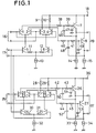
- FIG. 1 there is shown in circuit diagram a circuit construction of a quadrature demodulator to which the present invention is applied.
- the quadrature demodulator is an improvement to and includes common elements to those of the conventional quadrature demodulator described hereinabove with reference to FIG. 3.
- the quadrature demodulator includes first and second double differential circuits for inputting a local signal, a 90-degree phase shifted local signal and a modulated signal, which have similar constructions to those of the conventional quadrature demodulator, and overlapping description of the common construction is omitted herein to redundancy, but only differences of the quadrature demodulator from the conventional quadrature demodulator will be described below.
- like or corresponding elements to those of the conventional quadrature demodulator are denoted by like reference numerals to those of FIG. 3.
- the quadrature demodulator shown in FIG. 1 is different in construction from the conventional quadrature demodulator shown in FIG. 3 in that the first emitter follower circuit additionally includes resistors 38 to 41 and capacitors 46 to 49 and the second emitter follower circuit additionally includes resistors 42 to 45 and capacitors 50 to 53.
- An in-phase demodulation signal demodulated by the first double differential circuit and including unnecessary higher harmonic signals is inputted to a second-order active low-pass filter formed from the resistors 38 to 41, capacitors 46 to 49 and transistors 7 and 8.
- the unnecessary higher harmonic signals are removed from the in-phase demodulation signal by the second-order active low-pass filter, and a resulting signal from the second-order active low-pass filter is outputted to the output terminals 19.
- a 90-degree phase shifted demodulation signal demodulated by the second double differential circuit and including unnecessary higher harmonic signals is inputted to another second-order active low-pass filter formed from the resistors 42 to 45, capacitors 50 to 53 and transistors 26 and 27.
- the unnecessary higher harmonic signals are removed from the 90-degree phase shifted modulation signal by the second-order active low-pass filter, and a resulting signal from the second-order active low-pass filter is outputted to the output terminals 37.
- a desired in-phase demodulation output and a 90-degree phase shifted demodulation output which do not include unnecessary higher harmonic signals are obtained from the output terminals 19 and 37, respectively.
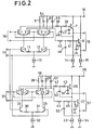
- FIG. 2 shows a circuit construction of a modification to the quadrature demodulator of the embodiment described above with reference to FIG. 1.
- the modified quadrature demodulator is different from the quadrature demodulator of the embodiment of FIG. 1 in that capacitors 54 and 55 are interposed between a power supply 18 and the outputs of the first double differential circuit while capacitors 56 and 57 are interposed between another power supply 36 and the outputs of the second double differential circuit.
- the capacitors 54 to 57 are provided additionally, the number of orders of active low-pass filters of the first and second double differential circuits is increased to 3, and consequently, unnecessary higher harmonics can be attenuated by a greater degree than those in the quadrature demodulator of the embodiment to FIG. 1.
Landscapes
- Engineering & Computer Science (AREA)
- Power Engineering (AREA)
- Networks Using Active Elements (AREA)
- Digital Transmission Methods That Use Modulated Carrier Waves (AREA)
- Semiconductor Integrated Circuits (AREA)
Applications Claiming Priority (3)
| Application Number | Priority Date | Filing Date | Title |
|---|---|---|---|
| JP32363095 | 1995-11-17 | ||
| JP7323630A JP2953365B2 (ja) | 1995-11-17 | 1995-11-17 | 直交復調器 |
| JP323630/95 | 1995-11-17 |
Publications (2)
| Publication Number | Publication Date |
|---|---|
| EP0774832A1 true EP0774832A1 (de) | 1997-05-21 |
| EP0774832B1 EP0774832B1 (de) | 2002-02-20 |
Family
ID=18156879
Family Applications (1)
| Application Number | Title | Priority Date | Filing Date |
|---|---|---|---|
| EP96118359A Expired - Lifetime EP0774832B1 (de) | 1995-11-17 | 1996-11-15 | Quadraturdemodulator |
Country Status (4)
| Country | Link |
|---|---|
| US (1) | US5734295A (de) |
| EP (1) | EP0774832B1 (de) |
| JP (1) | JP2953365B2 (de) |
| DE (1) | DE69619346T2 (de) |
Cited By (5)
| Publication number | Priority date | Publication date | Assignee | Title |
|---|---|---|---|---|
| FR2783110A1 (fr) * | 1998-09-08 | 2000-03-10 | Mitel Semiconductor Ltd | Dispositif de circuit melangeur a rejection d'image |
| WO2000019599A1 (de) * | 1998-09-30 | 2000-04-06 | Infineon Technologies Ag | Schaltungsanordnung zum mischen eines eingangssignals und eines oszillatorsignals miteinander |
| EP1067673A3 (de) * | 1999-06-30 | 2001-08-29 | Infineon Technologies AG | Mischer mit einstellbarer Linearität |
| EP1137168A3 (de) * | 2000-03-24 | 2003-10-15 | Nokia Corporation | Verfahren und Mischer zur Erzeugung eines Zwischenfrequenzsignals |
| EP1547258A4 (de) * | 2002-09-30 | 2006-08-09 | Skyworks Solutions Inc | Subharmonischer mischer |
Families Citing this family (2)
| Publication number | Priority date | Publication date | Assignee | Title |
|---|---|---|---|---|
| JPH11195940A (ja) * | 1998-01-06 | 1999-07-21 | Mitsubishi Electric Corp | 可変利得増幅器 |
| US7012343B2 (en) * | 2003-04-11 | 2006-03-14 | Micrel, Inc. | Resistance multiplier circuit and compact gain attenuator |
Citations (3)
| Publication number | Priority date | Publication date | Assignee | Title |
|---|---|---|---|---|
| EP0059000A1 (de) * | 1981-02-20 | 1982-09-01 | Philips Electronics Uk Limited | Direkter FM-Demodulator |
| EP0322157A1 (de) * | 1987-12-18 | 1989-06-28 | Rockwell International Corporation | Aktives Tiefpassfilter zur Verwendung mit Geräten für Hochfrequenzsignalquellen |
| WO1991003882A1 (en) * | 1989-08-30 | 1991-03-21 | At&E Corporation | Image canceling mixer circuit on an integrated circuit chip |
-
1995
- 1995-11-17 JP JP7323630A patent/JP2953365B2/ja not_active Expired - Fee Related
-
1996
- 1996-11-15 DE DE69619346T patent/DE69619346T2/de not_active Expired - Fee Related
- 1996-11-15 EP EP96118359A patent/EP0774832B1/de not_active Expired - Lifetime
- 1996-11-15 US US08/749,402 patent/US5734295A/en not_active Expired - Fee Related
Patent Citations (3)
| Publication number | Priority date | Publication date | Assignee | Title |
|---|---|---|---|---|
| EP0059000A1 (de) * | 1981-02-20 | 1982-09-01 | Philips Electronics Uk Limited | Direkter FM-Demodulator |
| EP0322157A1 (de) * | 1987-12-18 | 1989-06-28 | Rockwell International Corporation | Aktives Tiefpassfilter zur Verwendung mit Geräten für Hochfrequenzsignalquellen |
| WO1991003882A1 (en) * | 1989-08-30 | 1991-03-21 | At&E Corporation | Image canceling mixer circuit on an integrated circuit chip |
Non-Patent Citations (2)
| Title |
|---|
| CHAPOVSKIY AND LOVEYKO: "Q-Factor Instability of the Complex Conjugate Poles of an Emitter-Follower Active RC-Network", TELECOMMUNICATIONS AND RADIO ENGINEERING, vol. 24, no. 10, October 1969 (1969-10-01), WASHINGTON US, pages 139 - 140, XP002026238 * |
| MALIKOV, STUKALOV, MAMKOVA AND SHELEPOV: "A linear synchronous detector", TELECOMMUNICATIONS AND RADIO ENGINEERING, vol. 35/36, no. 1, January 1981 (1981-01-01), WASHINGTON US, pages 63 - 66, XP002026237 * |
Cited By (8)
| Publication number | Priority date | Publication date | Assignee | Title |
|---|---|---|---|---|
| FR2783110A1 (fr) * | 1998-09-08 | 2000-03-10 | Mitel Semiconductor Ltd | Dispositif de circuit melangeur a rejection d'image |
| WO2000019599A1 (de) * | 1998-09-30 | 2000-04-06 | Infineon Technologies Ag | Schaltungsanordnung zum mischen eines eingangssignals und eines oszillatorsignals miteinander |
| US6456144B2 (en) | 1998-09-30 | 2002-09-24 | Infineon Technologies Ag | Circuit configuration for mixing an input signal and an oscillator signal with one another |
| EP1067673A3 (de) * | 1999-06-30 | 2001-08-29 | Infineon Technologies AG | Mischer mit einstellbarer Linearität |
| US6650883B1 (en) | 1999-06-30 | 2003-11-18 | Infineon Technologies Ag | Mixer with adjustable linearity |
| EP1137168A3 (de) * | 2000-03-24 | 2003-10-15 | Nokia Corporation | Verfahren und Mischer zur Erzeugung eines Zwischenfrequenzsignals |
| US7151919B2 (en) | 2000-03-24 | 2006-12-19 | Nokia Corporation | Method for forming an intermediate frequency signal in a mixer, and a mixer |
| EP1547258A4 (de) * | 2002-09-30 | 2006-08-09 | Skyworks Solutions Inc | Subharmonischer mischer |
Also Published As
| Publication number | Publication date |
|---|---|
| US5734295A (en) | 1998-03-31 |
| EP0774832B1 (de) | 2002-02-20 |
| DE69619346T2 (de) | 2002-07-11 |
| JP2953365B2 (ja) | 1999-09-27 |
| DE69619346D1 (de) | 2002-03-28 |
| JPH09148847A (ja) | 1997-06-06 |
Similar Documents
| Publication | Publication Date | Title |
|---|---|---|
| US5329189A (en) | Mixer circuit | |
| US6993310B2 (en) | Current driven polyphase filters and method of operation | |
| KR100390257B1 (ko) | 반도체 회로 | |
| US20030025537A1 (en) | Frequency doubler circuit arrangement | |
| US5734295A (en) | Quadrature demodulator having active filters formed with emitter follower output stages | |
| US20020008983A1 (en) | Low-noise frequency converter with strong rejection of image frequency | |
| EP0522425B1 (de) | Einrichtung zur Erzeugung eines Signals | |
| EP0760554A1 (de) | Direktmischende, ein unsymmetrisches Signal empfangende und eine Ausgangsspannung mit minimierter Offsetspannung am Ausgang liefernde Frequenzmischschaltung | |
| CN101111996A (zh) | 主动式多相滤波器以及信号产生方法 | |
| JPH07283652A (ja) | 電圧制御キャパシタ | |
| JP2808927B2 (ja) | 周波数ディスクリミネータ | |
| JP3108551B2 (ja) | フィルタ回路 | |
| JP3736024B2 (ja) | ダブルバランスドミキサ | |
| US6897734B2 (en) | Integral mixer and oscillator device | |
| US4410979A (en) | Multiplexed signal receiver | |
| JP3230702B2 (ja) | 乗算回路 | |
| JPH073929B2 (ja) | Am検波回路 | |
| KR950005161B1 (ko) | Fm복조회로 | |
| JP2580122B2 (ja) | Fm復調回路 | |
| JPH02296408A (ja) | 差動増幅回路 | |
| JPH08298527A (ja) | デジタル位相変復調回路 | |
| JP2002076795A (ja) | 増幅回路及びそれを用いた衛星放送受信装置 | |
| JPS63102503A (ja) | 二重平衡変調回路 | |
| JPH0752810B2 (ja) | Fm直交復調器 | |
| JPH0998067A (ja) | 90度移相器 |
Legal Events
| Date | Code | Title | Description |
|---|---|---|---|
| PUAI | Public reference made under article 153(3) epc to a published international application that has entered the european phase |
Free format text: ORIGINAL CODE: 0009012 |
|
| AK | Designated contracting states |
Kind code of ref document: A1 Designated state(s): DE FR GB |
|
| 17P | Request for examination filed |
Effective date: 19970904 |
|
| 17Q | First examination report despatched |
Effective date: 20000228 |
|
| GRAG | Despatch of communication of intention to grant |
Free format text: ORIGINAL CODE: EPIDOS AGRA |
|
| GRAG | Despatch of communication of intention to grant |
Free format text: ORIGINAL CODE: EPIDOS AGRA |
|
| GRAH | Despatch of communication of intention to grant a patent |
Free format text: ORIGINAL CODE: EPIDOS IGRA |
|
| GRAH | Despatch of communication of intention to grant a patent |
Free format text: ORIGINAL CODE: EPIDOS IGRA |
|
| REG | Reference to a national code |
Ref country code: GB Ref legal event code: IF02 |
|
| GRAA | (expected) grant |
Free format text: ORIGINAL CODE: 0009210 |
|
| AK | Designated contracting states |
Kind code of ref document: B1 Designated state(s): DE FR GB |
|
| REF | Corresponds to: |
Ref document number: 69619346 Country of ref document: DE Date of ref document: 20020328 |
|
| ET | Fr: translation filed | ||
| PGFP | Annual fee paid to national office [announced via postgrant information from national office to epo] |
Ref country code: FR Payment date: 20021108 Year of fee payment: 7 |
|
| PGFP | Annual fee paid to national office [announced via postgrant information from national office to epo] |
Ref country code: GB Payment date: 20021113 Year of fee payment: 7 |
|
| PGFP | Annual fee paid to national office [announced via postgrant information from national office to epo] |
Ref country code: DE Payment date: 20021121 Year of fee payment: 7 |
|
| PLBE | No opposition filed within time limit |
Free format text: ORIGINAL CODE: 0009261 |
|
| STAA | Information on the status of an ep patent application or granted ep patent |
Free format text: STATUS: NO OPPOSITION FILED WITHIN TIME LIMIT |
|
| 26N | No opposition filed |
Effective date: 20021121 |
|
| REG | Reference to a national code |
Ref country code: GB Ref legal event code: 732E |
|
| REG | Reference to a national code |
Ref country code: FR Ref legal event code: TP |
|
| PG25 | Lapsed in a contracting state [announced via postgrant information from national office to epo] |
Ref country code: GB Free format text: LAPSE BECAUSE OF NON-PAYMENT OF DUE FEES Effective date: 20031115 |
|
| PG25 | Lapsed in a contracting state [announced via postgrant information from national office to epo] |
Ref country code: DE Free format text: LAPSE BECAUSE OF NON-PAYMENT OF DUE FEES Effective date: 20040602 |
|
| GBPC | Gb: european patent ceased through non-payment of renewal fee |
Effective date: 20031115 |
|
| PG25 | Lapsed in a contracting state [announced via postgrant information from national office to epo] |
Ref country code: FR Free format text: LAPSE BECAUSE OF NON-PAYMENT OF DUE FEES Effective date: 20040730 |
|
| REG | Reference to a national code |
Ref country code: FR Ref legal event code: ST |