EP0777164B1 - Elektrophotographisches Gerät - Google Patents
Elektrophotographisches Gerät Download PDFInfo
- Publication number
- EP0777164B1 EP0777164B1 EP96119236A EP96119236A EP0777164B1 EP 0777164 B1 EP0777164 B1 EP 0777164B1 EP 96119236 A EP96119236 A EP 96119236A EP 96119236 A EP96119236 A EP 96119236A EP 0777164 B1 EP0777164 B1 EP 0777164B1
- Authority
- EP
- European Patent Office
- Prior art keywords
- photo
- layer
- sensitive drum
- toner
- surface layer
- Prior art date
- Legal status (The legal status is an assumption and is not a legal conclusion. Google has not performed a legal analysis and makes no representation as to the accuracy of the status listed.)
- Expired - Lifetime
Links
Images
Classifications
-
- G—PHYSICS
- G03—PHOTOGRAPHY; CINEMATOGRAPHY; ANALOGOUS TECHNIQUES USING WAVES OTHER THAN OPTICAL WAVES; ELECTROGRAPHY; HOLOGRAPHY
- G03G—ELECTROGRAPHY; ELECTROPHOTOGRAPHY; MAGNETOGRAPHY
- G03G15/00—Apparatus for electrographic processes using a charge pattern
- G03G15/75—Details relating to xerographic drum, band or plate, e.g. replacing, testing
- G03G15/751—Details relating to xerographic drum, band or plate, e.g. replacing, testing relating to drum
-
- G—PHYSICS
- G03—PHOTOGRAPHY; CINEMATOGRAPHY; ANALOGOUS TECHNIQUES USING WAVES OTHER THAN OPTICAL WAVES; ELECTROGRAPHY; HOLOGRAPHY
- G03G—ELECTROGRAPHY; ELECTROPHOTOGRAPHY; MAGNETOGRAPHY
- G03G21/00—Arrangements not provided for by groups G03G13/00 - G03G19/00, e.g. cleaning, elimination of residual charge
- G03G21/20—Humidity or temperature control also ozone evacuation; Internal apparatus environment control
- G03G21/203—Humidity
-
- G—PHYSICS
- G03—PHOTOGRAPHY; CINEMATOGRAPHY; ANALOGOUS TECHNIQUES USING WAVES OTHER THAN OPTICAL WAVES; ELECTROGRAPHY; HOLOGRAPHY
- G03G—ELECTROGRAPHY; ELECTROPHOTOGRAPHY; MAGNETOGRAPHY
- G03G5/00—Recording-members for original recording by exposure, e.g. to light, to heat or to electrons; Manufacture thereof; Selection of materials therefor
- G03G5/02—Charge-receiving layers
- G03G5/04—Photoconductive layers; Charge-generation layers or charge-transporting layers; Additives therefor; Binders therefor
- G03G5/08—Photoconductive layers; Charge-generation layers or charge-transporting layers; Additives therefor; Binders therefor characterised by the photoconductive material being inorganic
- G03G5/082—Photoconductive layers; Charge-generation layers or charge-transporting layers; Additives therefor; Binders therefor characterised by the photoconductive material being inorganic and not being incorporated in a bonding material, e.g. vacuum deposited
- G03G5/08214—Silicon-based
- G03G5/08235—Silicon-based comprising three or four silicon-based layers
- G03G5/08242—Silicon-based comprising three or four silicon-based layers at least one with varying composition
Definitions
- This invention relates to such electrophotographic apparatuses as printers, copiers, facsimile apparatuses, etc. using amorphous Si drums.
- a well-known electrophotographic apparatuses perform a commonly termed Curlson process, i.e., it forms images by predetermined electrophotographic process with exposing, developing, transferring, cleaning (i.e., residual toner removing), discharging, charging and other processing means disposed around the outer periphery of a photo-sensitive drum.
- Curlson process i.e., it forms images by predetermined electrophotographic process with exposing, developing, transferring, cleaning (i.e., residual toner removing), discharging, charging and other processing means disposed around the outer periphery of a photo-sensitive drum.
- the photo-sensitive drum is usually charged uniformly by utilizing corona discharge.
- the corona discharge usually has to be done by applying a high voltage of 4 to 8 KV or above by wire application and the application of such a high voltage by corona discharge causes oxidation of the photo-sensitive drum and generation of ozone, as well as resulting in the generation of such discharge products as oxygen nitride and ammonium salt. These substances are adsorbed to the drum surface to cause ready flow of image. Pronounced flow of image is caused remarkably in high humidity environments.
- the system uses a conductive drum, which is held in contact with the conductive roller on the photo-sensitive drum so as to apply it with a DC voltage by contact charging in darkness.
- the particle charging means requires a charging vessel being accommodating charging particles in such a situation having an opening facing the drum. Therefore, it is complicated to deal with the charging vessel. Besides, the particles should always been charged uniformly in frictional contact with the photo-sensitive drum, thus resulting in fatigue in long use. This means poor durability of the particle charging means.
- Recent electrophotographic apparatuses use amorphous Si drums in order to improve the durability and make the maintenance unnecessary.
- amorphous Si highly absorbs moisture compared to OPC and other organic semiconductors, and amorphous Si drums apt to generate more flow of image.
- the photo-sensitive drum is heated by a sheet heater or like heating member provided on its back side.
- the heater is used, however, heat control means or the like has to be provided and complicates the system construction. Particularly, when a copier, a printer, etc. is to be reduced in size or personalized, the system construction complication by providing the heater is inevitable.
- the heater poses a further problem that its temperature elevation requires a certain time, i.e., a considerably long time (warm-up time), from the instant of the power-"on" till it is ready to start the printing. Besides, this warm-up time means corresponding power consumption.
- the photo-sensitive drum is heated to raise its temperature up to the neighborhood of the TG temperature (glass transition temperature) of the toner, thus such various problems generate as resulting in toner attachment to its surface.
- Japanese Laid-Open Patent Publication No. 62-272275 proposes a photo-sensitive drum, which uses a surface layer covering an amorphous Si photoconductive layer.
- the surface layer is made of an amorphous material mainly composed of silicon (Si) and carbon (C) and containing oxygen (O), hydrogen (H) and fluorine (F) and has a dynamic indentation hardness of 300 to 1,000 kgf/mm 2 .
- the dynamic indentation hardness is set in the above range for the following grounds.
- a dynamic indentation hardness exceed 1,000 kgf/mm 2
- the surface layer has a so high Si content that it is subject to chemical influence and gives rise to the image defect as noted above.
- a dynamic indentation hardness lower than 300 kgf/mm 2 on the other hand, the surface layer has a high C content, deteriorating the photoconductivity and increasing residual potential.
- the hardness is considerably reduced to increase the wear of the surface layer in an image copying process and readily give rise to image defect.
- the techniques realize commonly called heater-less photo-sensitive drums by taking only the drum surface layer into considerations.
- the flow of image is caused not only by the surface layer but also is determined by the relation between the photo-sensitive drum and the developing means, the transferring means and other processing means.
- the above disclosed technique seeks to prevent the flow of image particularly due to high humidity rise while avoiding the wear of the photo-sensitive drum surface layer.
- the flow of image is caused by reduction of the photo-sensitive drum surface layer potential with drum surface resistance reduction in a high humidity environment, which is attributable to an increase of the moisture absorption of the photo-sensitive drum surface due to drum surface deterioration and attachment to the drum surface of discharge products caused by ozone generation due to the discharge phenomenon when charging the drum.
- the discharge products are attached to the drum surface layer contrived in any way, and accumulated while the photo-sensitive drum is in use.
- the generation of the flow of image depends on the accumulation degree of the attached substances, making it difficult to ensure stable image formation for long time.
- Japanese Laid-Open Patent Publication No. 61-278861 proposes a technique, in which the photo-sensitive drum surface is cleaned by using a cleaning material as cleaning auxiliary agent.
- the cleaning material is prepared by adding to the developer strontium titanate having the reversed polarity of charging to the toner.
- the reversed polarity strontium titanate is a highly resistive or insulating dielectric. Therefore, it causes instable charging of the toner during the development and fog or like image defect.
- Publication No. 7-17526 an electrophotographic apparatus, in which a photoconductive layer supported on a base is charged uniformly by means including discharge phenomenon while writing on the charged photoconductive layer an exposure image, a toner image is formed by inverse development.
- the photoconductive layer of the amorphous Si photo-sensitive drum as noted above is formed as an amorphous Si layer with a thickness of 25 ⁇ m or below, preferably 2 to 20 ⁇ m, and the surface potential of approximately 360 V or below is generated by charging the layer.
- EP-A-0 679 952 discloses an electrophotographic apparatus with a photo-sensitive drum having a small a-Si layer covered by a SiC layer.
- a developer is used which includes a polishing agent to treat the drum surface.
- Softer polishing agents for polishing an a-Si photosensive drum are disclosed in US-4,764,448.
- JP-A-7-152196 discloses again harder abrasive particles in the developer to remove the oxidised surface layer of an amorphous silicon photosensitive, drum.
- the use of an abrasive to clean a sleeve for feeding toner to a photosensitive drum is disclosed in US-4,891,294.
- Photosensitive drums with hard protective surface layers are further disclosed in US-5,352,555 and JP-2-154275.
- An embodiment provides an electrophotographic apparatus, which permits formation of sharp images without flow of image or fog particularly with an amorphous Si photo-sensitive drum which is charged uniformly by means including such discharge phenomenon as specially a corona charger, a charging roller or a charging brush.
- Another embodiment of the invention provides an electrophotographic apparatus, which can be used for long time with a developer incorporating a cleaning auxiliary agent or an abrasive to form sharp images.
- a further embodiment of the invention provides an electrophotographic apparatus using an amorphous Si drum, which permits formation of sharp images without flow of image or fog irrespective of temperature or like environmental condition changes, as well as permitting simplification of the construction and reinforcement of the stability.
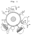
- the amorphous Si photo-sensitive drum has a photoconductive layer 1b and a surface layer 1c, these layers 1b and 1c being laminated on a conductive base 1a in the form of an aluminum cylinder.
- the surface layer 1c is made of an ⁇ -SiC type inorganic highly resistive or insulating material to maintain the surface potential V 0 and latent image potential distribution on the photoconductive layer 1b.
- a highly resistive or insulating toner is used for the developer to develop the latent image.
- the toner in this case contains dew condensation or moisture, its attachment to the photo-sensitive drum surface layer 1c results in the generation of flow of image.
- the invention seeks to provide an electrophotographic apparatus, which permits formation of sharp images without flow of image or fog, by effectively combining the photoconductive layer 1b, surface 1c and developing conditions.
- a preferred embodiment of the invention is an electrophotographic apparatus, in which a photo-sensitive drum having a photoconductive layer and a surface layer, these layers being laminated on a base, and a latent image formed on above photo-sensitive drum is developed by causing selective attached toner, the apparatus comprising:
- the surface layer 1c has a dynamic indentation hardness of 490 to 1960 MPa (50 to 200 kgf/mm 2 ) on the surface side, and has a thickness of 0.4 to 1.2 ⁇ m, preferably 0.5 to 0.8 ⁇ m.
- a second sub-layer which is formed on the outer surface side has a dynamic indentation hardness of 50 to 200 kgf/mm 2 and a thickness of 800 to 3,000 ⁇ (angstroms), and a first sub-layer formed on the inner or bottom side is harder than the second sub-layer.
- the rubbing of the photo-sensitive drum by the developer with the dew condensation promotes the generation of discharge products.
- the above phenomenon may occur when the above temperature difference is attributable to a high temperature of the developer (i.e., developer vessel).
- the photo-sensitive drum surface temperature is held at approximately 0 to +10°C above the temperature in the developer vessel.
- the photo-sensitive drum surface layer is polished in an initial stage of the image formation.
- the photo-sensitive drum surface layer 1c is formed by glow discharge decomposition or the like, discharge products such as ion nitrate and ammonium ions generated by corona discharge are adsorbed to molecule ends or the like in micro-interstices on the surface of the surface layer 1c, thus giving rise to the above problem.
- the surface layer 1c is polished in order to remove the discharge products which may be adsorbed in an initial stage of the image formation.
- the dynamic indentation hardness of the surface layer 1c is set to 2940 MPa (300 kgf/mm 2 ) or below on the surface side.
- polishing means caused to polish the photo-sensitive drum surface layer 1c having the micro-interstices at least in those initial stage for the image formation.
- the hardness of the surface layer 1c is made to increase as one goes inward toward the inner side of the photoconductive layer 1b from the surface side.
- the grinding rate can be reduced progressively as one goes inward, and this enables maintaining long life or high durability.
- the content of amorphous carbon in the surface layer 1c is set to be so high that the surface layer is represented by an elementary ratio composition formula ( a-Si 1-x C x :H ), x being 0.95 ⁇ x ⁇ 1.
- the grain size in a range of 0.05 to 5 ⁇ m, preferably 0.1 to 3 ⁇ m.
- the relation between the surface layer 1c and the photoconductive layer 1b is considered.
- the photo-sensitive drum is heater-less, its temperature depends on the temperature in the apparatus. This means that it is necessary that no great photo-sensitive surface potential changes are caused by temperature changes.
- the thickness of the photoconductive layer 1b covered by the surface layer 1c is preferably 50 ⁇ m or below.
- the photo-sensitive surface potential is not changed greatly, for instance by about 10 %, with a temperature change by reducing the surface potential to around 400 V and setting the photo-sensitive drum thickness to about 40 ⁇ m.
- the breakdown voltage of its layer is 12 to 16 V/ ⁇ m. With the thickness set to 50 ⁇ m or below, it is thus possible to suppress the flow of image and prevent the breakdown voltage deterioration in long use by setting the surface potential V 0 to 800 V, preferably 600 V or below.
- the lower limit of the thickness is suitably set to 2 to 3 ⁇ m, because of the fact that the thickness of, for instance, an a-Si:H layer corresponding to 90 % absorption of incident light is about 2.2 ⁇ m.
- image formation without fog or the like is obtainable without use of any heater. It is thus possible to greatly reduce power consumption. Besides, since no heater is used, it is not necessary to use such components as a thermistor for detecting the drum surface temperature and a controller for controlling any heater according to the temperature detected by such a thermistor. The circuit construction thus can be simplified. Moreover, no heater warm-up time is needed, thus greatly reducing the start time of the apparatus.
- Japanese Laid-Open Patent Publication No. 61-278861 shows a technique employing developing means, which is constructed such as to perform development by causing a developer incorporating an abrasive to rub the photo-sensitive drum and has a polishing function to remove discharge products.
- the abrasive incorporated is a highly resistive or insulating material having the opposite charging polarity to the toner. Therefore, in the development it makes the charge on the toner unstable, thus resulting in such image detect as fog.
- the abrasive particles are made finer than the toner particle size, and this finer particle abrasive and an aggregate thereof are used to provide a cleaning effect.
- This means that the abrasive is attached together with toner to the photo-sensitive drum. Since the downstream side transfer step executes electrostatic transfer with an applied bias voltage of the opposite polarity to the toner, the abrasive is transferred together with toner and causes such image sharpness reduction as white spots or white areas.
- the abrasive has an adequate particle size with respect to the toner and is conductive, and :it is held on the toner in the development. Thus, it does not remain so much in the developing unit.
- the conductive abrasive used according to the embodiment is effectively prevented from being transferred in the transfer step.
- a preferred embodiment of the invention resides in an electrophotographic apparatus, in which a photo-sensitive drum having a photoconductive layer and a surface layer, these layers being laminated on a base, and a latent image formed on above photo-sensitive drum is developed by selective attached toner, the apparatus comprising;
- the conductive abrasive may be used silicon carbide (SiC), magnetite (Fe 3 O 4 ), tin oxide (SnO 2 ), tin carbide (TiC) and inorganic particles obtained by treating highly resistive particles to be conductive. These abrasive is by no means limitative.
- the conductive abrasive suitably has a grain size of 0.05 to 5 ⁇ m, preferably 0.1 to 3 ⁇ m.
- the resistivity of the abrasive is set to 10 2 to 10 10 ⁇ cm.
- the resistivity of the transferred material exceeds 10 10 ⁇ cm, the transfer efficiency of the transfer process after the development is quickly reduced as is well known in the art.
- the resistivity is no higher than 10 2 ⁇ cm, the charging property of the toner is too poor to obtain sufficient developing performance, although depending on the amount of the abrasive added.
- the abrasive After the transfer, the abrasive reaches a toner scraper of a cleaning blade together with the toner, and is partly scraped off while partly being held on the end of the blade and continuing the polishing.
- a rubbing roller may be effectively provided in front of the cleaning blade to hold the toner and the abrasive on its surface and rub the photo-sensitive drum with the abrasive having been held, thus effecting the polishing.
- the transfer roller is rotated at a slightly higher peripheral speed than the peripheral speed of the photo-sensitive drum to obtain effective separation of the toner and the abrasive during the transfer.
- the back side of a transfer medium is held at a high potential to cause transfer of toner from the photo-sensitive drum to the transfer medium.
- the abrasive particles which have been brought together with toner to the drum are suitably not readily transferred compared to the toner, and its great proportion remains on the drum surface and is suitably removed by the cleaning means in the subsequent step while polishing the drum surface.
- This function is attributable to the low resistivity of the toner and also to the optimum particle size ratio between the toner and the abrasive (i.e., cleaning particle).
- the abrasive particles When the abrasive particles are too small compared to the toner particles, they are readily held on the toner particle surface and moved with the toner during the development and transfer. Consequently, less abrasive remains on the photo-sensitive drum surface after the transfer. When the abrasive particles are too large, white spots and white areas are generated in the image area by the abrasive particles having been transferred to the drum. When the particle size ratio between the toner and the abrasive is adequate, no white spot or white area or like image defect is generated, and much abrasive particles can be held on the drum surface after the transfer.
- the particle size range and proportion of the abrasive particles are defined accordingly; the average particle size ratio between the toner and the abrasive in the developer is set in a range of 100 : 1 to 2 : 1, more preferably 50 : 1 to 3 : 1, and the abrasive particles are added in a range of 0.3 to 5 % to the toner in the developer.
- the surface layer of the photo-sensitive drum is represented by an elementary ratio composition formula ( a-Si 1-x C x :H ), x being 0.95 ⁇ x ⁇ 1, and has a dynamic indentation hardness of 300 kgf/mm 2 or below, the hardness of the surface layer being higher on the inner side of the photoconductive layer than on its outer surface side and preferably gradually increasing as one goes inward from the outer surface side toward the inner side of the photoconductive layer.
- the surface layer 1c has a dynamic indentation hardness of 50 to 200 kgf/mm 2 on its outer surface side and a thickness of 0.4 to 1.2 ⁇ m, preferably 0.5 to 0.8 ⁇ m.
- a second sub-layer on the upper surface side has a dynamic indentation hardness of 50 to 200 kgf/mm 2 and a thickness of 800 to 3,000 nm, and the first layer on the inner side is harder than the second sub-layer on the surface.
- a photo-sensitive drum at la a conductive base, 1b a photoconductive layer, at 1c a surface layer, 1c 1 a first sub-layer, 1c 2 a second sub-layer, 2 an exposing head, 3 an optical system, 4 a two-component developing unit, 41 a developer vessel, and 8 a charging unit.
- an electrophotographic apparatus is shown, to which the invention is applied.
- an optical system including an LED exposing head 2 and a selfoc lens 3, a developing unit 4, a transfer roller 5, a cleaning blade 6, a discharging lamp 7, and a charging unit 8, are disposed around an a-Si photo-sensitive drum 1, which rotates clockwise in the figure, in the mentioned order in the rotating direction.
- the photo-sensitive drum 1 has a photoconductive layer 1b and a surface layer 1c, these layers 1b and 1c being laminated on a photoconductive base or support la, a carrier injection prevention layer 1e intervening between the conductive support la and the photoconductive layer 1b, and a transition layer 1f intervening between the photoconductive layer 1b and the surface layer 1c.
- the support la is cylinder having an aluminum character, made of such a metallic material as SUS, Ti, Ni, Au, Ag, etc., an inorganic material such as glass with a conductive surface film, a transparent resin such as epoxy or the like.
- the support la has a thickness of 3 mm, an outer diameter of 30 mm and an axial length dimension of 254 mm.
- the carrier injection prevention layer 1e may be made of various materials depending on the material of the photoconductive layer 1b. Where the photoconductive layer 1b is made of an amorphous Si type material, the carrier injection prevention layer 1e is suitably made of like amorphous Si type material.
- the amorphous Si type photoconductive layer 1b is formed by a glow discharge decomposition process, a sputtering process, an ECR process, a deposition process or like process. It suitably contains 5 to 40 % by weight of a dangling bond end element, such as hydrogen (H) or a halogen, introduced in its formation.
- a dangling bond end element such as hydrogen (H) or a halogen
- the photoconductive layer 1b is made of a photoconductor represented as a-Si:H.
- the layer 1b is suitably non-doped or doped with a Va family element to increase the mobility of electrons.
- the developing bias is negative, it suitably contains a IIIa family element to increase the mobility of positive holes. If necessary, it may contain such element as C, O, N, etc. to obtain desired electric characteristics such as dark conductivity or photoconductivity, optical band gap, etc.
- the thickness of the entirety of the photoconductive layer 1b is suitably 3 to 50 ⁇ m in view of ensuring the necessary charging voltage or breakdown voltage or absorption of exposure light or suppressing the residual potential noted above. Why this is so will be described later.
- the surface layer 1c is formed by a glow discharge decomposition process, a sputtering process, an ECR process, a deposition process or the like. It is made of hydroxidic amorphous silicon carbide represented by an elementary ratio composition formula ( a-Si 1-x C x :H ), x being 0.95 ⁇ x ⁇ 1, and has a dynamic indentation hardness of 50 to 200 kgf/mm 2 on its outer surface (or free surface layer). Particularly, it has a resistivity of 10 12 to 10 13 ⁇ cm.
- the hardness of the surface layer 1c is increased gradually as one goes inward from the outer surface side toward the inner side of the photoconductive layer 1b.
- Such a hardness gradient may be provided when forming the surface layer 1c by, for instance, the glow discharge decomposition process by such means as gradually increasing the ratio of C-containing gas to Si-containing gas in the material gas, gradually increasing the layer formation gas pressure, gradually reducing the factor of dilution of the material gas by hydrogen gas, gradually reducing the discharge power, or gradually reducing the temperature of the aluminum character cylinder drum base.
- the surface layer 1c suitably has a thickness of 0.4 to 1.2 ⁇ m, preferably 0.5 to 0.8 ⁇ m.
- the surface layer 1c is polished. For this reason, with a thickness below 0.4 ⁇ m a sufficient hardness gradient cannot be obtained. Therefore, the durability is insufficient, and image streaks or the like are generated when the number of prints is increased. With a thickness above 1.2 ⁇ m the residual potential on the side of the photoconductive layer 1b is so high as to cause fog or like image detect.
- the transition layer 1f which has less C content in a-SiC:H than the surface layer 1c, is suitably provided between the photoconductive layer 1b and the surface layer 1c.
- the thickness of the transition layer 1f is set to 1 ⁇ m or below, preferably 0.05 to 0.5 ⁇ m.
- the surface layer 1c may have a two-layer structure instead of the uni-layer structure.
- the surface layer 1c may comprise a first sub-layer 1c 1 on the side of the photoconductive layer 1b and a second sub-layer 1c 2 on the upper or free surface side.
- the second sub-layer 1c 2 is represented by a elementary ratio composition a formula (a-Si 1-x C x :H), x being 0.95 ⁇ x ⁇ 1, has a dynamic indentation hardness of 50 to 200 kgf/mm 2 , and a thickness of 800 to 3,000 angstroms.
- the inner side first layer 1c 1 is harder than the second sub-layer 1c 2 .
- the dynamic indentation hardness of the first sub-layer 1c 1 is 300 kgf/mm 2 or above. With this hardness, the sub-layer is capable of being polished by abrasive or the like without being worn out.
- the polishing is stopped by the inner side first sub-layer 1c1 in its stage, in which the surface has been smoothed. Thus, life extension can be obtained.
- the total thickness of the first and second sub-layers 1c 1 and 1c 2 i.e., the thickness of the surface layer 1c, is set to 0.4 to 1.2 ⁇ m, preferably 0.5 to 0.8 ⁇ m.
- the carrier injection prevention layer 1e may be made of various materials depending on the material of the photoconductive layer 1b. Where an amorphous Si type material is used for the photoconductive layer 1b, like amorphous Si type material is suitably used for the carrier injection prevention layer 1e.
- the a-Si:H photoconductive layer 1b and the SiC surface layer 1c are laminated by using a capacitance-coupled glow discharge decomposition process.
- the photo-sensitive drum 1 was fabricated by setting the thickness of the photoconductive layer 1b to 15, 25, 40 and 60 ⁇ m as will be described later.
- the surface layer 1c was formed only with a uni-layer structure layer without forming a two-layer constructure layer, and its thickness was set to 0.6 ⁇ m.
- the LED exposing head 2 is fabricated as a head array with an exposure wavelength of 685 nm and driven by dynamic driving for time-division exposure of 40 times 64 bits for each scanning line.
- the developing unit 4 includes a developer vessel 41 accommodating a multi-component developer composed of carrier and toner, and a developing roller 42 accommodating a stationary magnet 43.
- a DC developing bias power supply 44 capable of setting a selected bias voltage between 50 to 1200 V, for instance, is connected to the developing roller 42.
- the two-component developer is by no means limitative.
- the transfer roller 5 As the transfer roller 5 a conductive roller is used to increase the transfer efficiency.
- the transfer roller 5 is biased by a transfer bias of the reversed polarity to the toner charging potential, and is rotated in uniform forced contact with the periphery of the photo-sensitive drum 1. It is rotated at one of two speeds, that is, it is rotated either in synchronism to the drum 1 (transfer step in contrast examples) or at a slightly higher peripheral speed, specifically by 1 to 5 %, than the peripheral speed of the drum 1 (transfer step in embodiment examples).
- the charging unit 8 is a well-known corotron charger to uniformly charge the photo-sensitive drum 1.
- reference numeral 81 designates a corona charger, 82 a control grid, 83 a discharge bias, and 84 a charging control bias.
- the photo-sensitive drum 1 was charged to a surface potential V 0 shown below by applying a high discharge bias voltage with the charging control bias set to an adequate value in a range of around 150 to 1,200 V, and then exposed to a predetermined latent image by the exposing head 2, and the latent image thus formed developed in the developing unit 4 to obtain a toner image which was then transferred to the transfer roller 5.
- the transfer voltage applied to the transfer roller back surface side was set to -800 V, slightly higher than the drum surface potential by holding the charging control bias constant.
- the peripheral speed of the transfer roller is set to be higher by about 1 % than the peripheral speed of the drum.
- Example 1 (using a two-component developer):
- Toner composition Styrene acryle resin 100 constructive ratio Nygrocin dye 3 constructive ratio Polypropyrene wax 5 constructive ratio Carbon black 8 constructive ratio
- the mixture of this composition was fused and kneaded using a two-axis extruder. The mixture was then cooled down and coarsely commuted to a medium particle size. The particles were then finely commuted by jet mill to obtain toner with an average particle size of 7 ⁇ m.
- the two-component developer was prepared by mixing 5 constructive ratio of the toner thus obtained and 95 constructive ratio of a carrier.
- the developer was used with the image forming apparatus as described above, and image evaluation was made.
- Example 2 (using a uni-component developer):
- a toner with an average particle size of 7 ⁇ m was prepared by the same test as in Example 1.
- To this toner were added 0.5 % of hydrophobic silica and one constructive ratio of conductive TiO 2 abrasive with a particle size of 0.7 ⁇ m (particle size ratio of 1 : 10) and a resistivity of 10 5 ⁇ cm, and the admixture was kneaded using a Henshell mixer.
- Example 3 (using a uni-component developer):
- Example 2 The same experiment as in Example 2 was conducted except for adding 2 % of TiC abrasive with a particle size of 0.2 ⁇ m and a resistivity of 10 3 ⁇ cm. No abnormality of image and drum surface was observed.
- Image evaluation was made in the same manner as in Example 2 for adding, in lieu of the TiO 2 abrasive, the same amount of SiO 2 with a particle size of 0.5 ⁇ m and a resistivity of 10 12 ⁇ cm. Sharp image could not be obtained due to generation of flow of image. Also, cloud was formed on the drum surface.
- Image evaluation was made in the same manner as in Example 2 for using, in lieu of the TiO 2 abrasive, the same amount of strontium titanate with a particle size of 1 ⁇ m and a resistivity of 10 12 ⁇ cm. Sharp image could not be obtained due to generation of flow of image.
- Example 2 The same test as in Example 2 was made except for using a TiO 2 abrasive with a particle size of 4 ⁇ m (particle size ratio of 1 : 1.75) and a resistivity of 10 4 ⁇ cm. Full image with white spots was produced.
- Example 1 A further experiment was conducted by using the developer in Example 1.
- the surface potential V 0 on the photo-sensitive drum 1 was set to 600 V by adjusting the charging control bias, etc, and then the transfer voltage applied to the transfer roller back surface side was set to -800 V, slightly higher than the drum surface potential by holding the charging control bias constant.
- the peripheral speeds of the drum and the transfer roller were synchronized. Full image with slight white spots was produced, and the image sharpness was reduced compared to the case of Example 2.
- the carrier was a ferrite carrier with an average particle size of 70 ⁇ m.
- the ferrite carrier is by no means limitative, and may be replaced with such carriers as iron particles, magnetite, etc., or magnetic resin carriers.
- the toner used as magnetic toner was a highly resistive or insulating toner, which was formed by adding a binder resin, a coloring agent, a charge control agent, an anti-off-set agent, etc. to a magnetic material and had an average particle size of 5 to 15 ⁇ m.
- a toner (hereinafter referred to as A toner) incorporating an abrasive (hereinafter referred to as A abrasive) having added a conductive titanium oxide, as an abrasive/fluidity promoter having a specific surface area of 40 to 60 m 2 /g, a resistivity of 10 3 ⁇ cm, a hydrophobic degree of 0 %, a water content of 1.0 %, surface treatment Sd doping of SiO 2 and an average particle size 0.1 ⁇ m.
- a toner incorporating an abrasive (hereinafter referred to as A abrasive) having added a conductive titanium oxide, as an abrasive/fluidity promoter having a specific surface area of 40 to 60 m 2 /g, a resistivity of 10 3 ⁇ cm, a hydrophobic degree of 0 %, a water content of 1.0 %, surface treatment Sd doping of SiO 2 and an average particle size 0.1 ⁇
- B toner (hereinafter referred to as B toner) incorporating an abrasive (hereinafter referred to as B abrasive) as a conductive titanium oxide having a specific surface area of 10 to 15 m 2 /g, a resistivity of 10 3 ⁇ cm, a hydrophobic degree of 0 %, a water content of 0.5 %, surface treatment doping of SiO 2 and an average particle size of 0.3 ⁇ m, and C toner (hereinafter referred to as C toner) free from any incorporated abrasive.
- the adequate mixture ratio between the carrier and the toner was set to 85 - 90 to 15 - 10 % by weight.
- the effect of the invention was confirmed with respect to the A toner as follows.
- the surface potential V 0 on the photo-sensitive drum 1 was set to 450 V
- the developing bias was set to 250 V
- the temperature of the developer in the developer vessel 41 was set to 20°C by providing a heater (not shown) in the developer vessel 41.
- the apparatus was left for more than 2 hours in a room, which was held at temperatures of 10, 20, 25 and 30°C respectively under a medium relative humidity set by an air conditioner, and then 10,000 prints were produced at each temperature of the apparatus noted above.
- the apparatus temperature of 10°C slight flow of image was generated in an initial printing stage up to 10,000 prints.
- no image defect was produced.
- drum thinner it is thus possible to suppress the drum surface potential variations with environmental condition variations by making the drum thinner to be 50 ⁇ m or below, preferably 40 ⁇ m or below.
- the effects of the toner confirmed with the B and C toners by using a 25 ⁇ m photo-sensitive drum were as follows.
- the drum surface potential V 0 was set to 450 V without providing any heater in the photo-sensitive drum, and printing was done while varying the apparatus temperature from 10 to 40°C with a temperature gradient of 10°C/hour under the medium relative humidity. Slight flow of image was generated in an initial stage of production of 10,000 prints only in the case of the C toner free from abrasive, but no flow of image was observed at the end of production of 100,000 prints.
- the electrophotographic apparatus which uses an amorphous Si drum which is uniformly charged by means having resort to the discharge phenomenon, such as a corona discharger, a charging roller, or a charging brush, it is possible to obtain sharp image free from flow of image or fog.
- the discharge phenomenon such as a corona discharger, a charging roller, or a charging brush
- the electrophotographic apparatus which uses an amorphous Si drum, it is possible to form a sharp image without fog or flow of image irrespective of such environmental condition change as temperature etc., taking into consideration simplification of the construction and reinforcement of the stability.
Landscapes
- Physics & Mathematics (AREA)
- General Physics & Mathematics (AREA)
- Chemical & Material Sciences (AREA)
- Inorganic Chemistry (AREA)
- Atmospheric Sciences (AREA)
- Engineering & Computer Science (AREA)
- Life Sciences & Earth Sciences (AREA)
- Biodiversity & Conservation Biology (AREA)
- Ecology (AREA)
- Environmental & Geological Engineering (AREA)
- Environmental Sciences (AREA)
- Photoreceptors In Electrophotography (AREA)
- Developing Agents For Electrophotography (AREA)
Claims (9)
- Elektrophotographische Vorrichtung, in der ein auf einer photoempfindlichen Trommel gebildetes latentes Bild durch selektive Toneranhaftung entwickelt wird, aufweisend:wobei die Temperatur der Oberfläche der photoempfindlichen Trommel etwa in einem Bereich von 0 bis +10°C des Entwicklerbehälters gehalten wird.eine elektrophotographische photoempfindliche Trommel mit einer photoleitfähigen Schicht (1b) und einer Oberflächenschicht (1c, 1c1, 1c2), wobei die Schichten auf einem Träger (1a) laminiert sind, die Oberflächenschicht durch die Zusammensetzungsformel für das Elementenverhältnis a-Si1-xCx:H mit 0,95 ≤ x < 1 wiedergegeben ist, die dynamische Eindrückhärte der Oberflächenschicht auf ihrer äußeren Oberfläche 2940 MPa (300 kgf/mm2) oder weniger beträgt und die Härte der Oberflächenschicht auf der Innenseite zur photoleitfähigen Schicht hin höher als auf der äußeren Oberflächenseite ist, undeine Entwicklungseinheit (4) mit einem Entwicklerbehälter (41), der einen Entwickler zur Entwicklung des latenten Bilds enthält, der einen Toner und ein abrasives Mittel zum Reiben der Oberfläche der photoempfindlichen Trommel enthält, das in dem Entwicklerbehälter (41) rückgewonnen wird,
- Elektrophotographische Vorrichtung, in der ein auf einer photoempfindlichen Trommel gebildetes latentes Bild durch selektive Toneranhaftung entwickelt wird, aufweisend:eine Entwicklungseinheit (4) zur Entwicklung des latenten Bilds mit einem Entwickler, der ein leitfähiges Abrasivmittel mit einer Volumenleitfähigkeit von 102 bis 1010 Ω·cm enthält, undeine elektrophotographische photoempfindliche Trommel mit einer photoleitfähigen Schicht (1b) und einer Oberflächenschicht (1c, 1c1, 1c2), wobei die Schichten auf einem Träger (1a) laminiert sind, die Oberflächenschicht (1c, 1c1, 1c2) durch die Zusammensetzungsformel für das Elementenverhältnis a-Si1-xCx:H mit 0,95 ≤ x < 1 wiedergegeben ist und zumindest auf einer äußeren Oberflächenseite eine ausreichende Härte aufweist, um durch das Abrasivmittel poliert zu werden, die dynamische Eindrückhärte der Oberflächenschicht auf ihrer äußeren Oberfläche 2940 MPa (300 kgf/mm2) oder weniger beträgt und die Härte der Oberflächenschicht auf der Innenseite zur photoleitfähigen Schicht hin höher als auf der äußeren Oberflächenseite ist.
- Vorrichtung nach Anspruch 1 oder 2, wobei die Härte der Oberflächenschicht (1c, 1c1, 1c2) von der äußeren Oberflächenseite zur Innenseite bei der photoleitfähigen Schicht (1b) hin graduell zunimmt und
das Bild auf de Oberflächenschicht (1c, 1c1, 1c2) gebildet wird, während diese zumindest in einer anfänglichen Stufe der Bildbildung poliert wird. - Vorrichtung nach einem der Ansprüche 1 bis 3, wobei die photoleitfähige Schicht (1b) eine amorphe Si-Schicht mit einer Dicke von 2 bis 50 µm ist und das Oberflächenpotential der photoempfindlichen Trommel auf etwa 800 V oder weniger festgesetzt wird.
- Vorrichtung nach einem der Ansprüche 1 bis 4, wobei die Härte einer inneren Oberflächenschicht von der Seite der äußeren Oberfläche zur Innenseite bei der photoleitfähigen Schicht (1b) hin graduell zunimmt.
- Vorrichtung nach einem der Ansprüche 1 bis 5 mit einer Transferrolle (5), die mit einer etwas höheren Umfangsgeschwindigkeit als der der photoempfindlichen Trommel gedreht wird.
- Vorrichtung nach einem der Ansprüche 1 bis 6, wobei das mittlere Teilchengrößenverhältnis zwischen Toner und Abrasivmittelteilchen in dem Entwickler von 100 : 1 bis 2 : 1, vorzugsweise von 50 : 1 bis 3 : 1 reicht.
- Vorrichtung nach einem der Ansprüche 1 bis 7, wobei der Entwickler 0,3 bis 5% Abrasivmittelteilchen bezüglich des Toners enthält.
- Vorrichtung nach einem der Ansprüche 1 bis 8, wobei die Rückseite eines Transfermediums bezüglich des Potentials der Oberfläche der photoempfindlichen Trommel in einem Transferprozeß auf einem hohen Potential gehalten wird.
Applications Claiming Priority (6)
| Application Number | Priority Date | Filing Date | Title |
|---|---|---|---|
| JP33416395 | 1995-11-29 | ||
| JP33416395A JP3330009B2 (ja) | 1995-11-29 | 1995-11-29 | 電子写真装置 |
| JP334163/95 | 1995-11-29 | ||
| JP33411495A JP3330008B2 (ja) | 1995-11-29 | 1995-11-29 | 電子写真装置 |
| JP334114/95 | 1995-11-29 | ||
| JP33411495 | 1995-11-29 |
Publications (3)
| Publication Number | Publication Date |
|---|---|
| EP0777164A2 EP0777164A2 (de) | 1997-06-04 |
| EP0777164A3 EP0777164A3 (de) | 2001-02-14 |
| EP0777164B1 true EP0777164B1 (de) | 2004-03-24 |
Family
ID=26574735
Family Applications (1)
| Application Number | Title | Priority Date | Filing Date |
|---|---|---|---|
| EP96119236A Expired - Lifetime EP0777164B1 (de) | 1995-11-29 | 1996-11-29 | Elektrophotographisches Gerät |
Country Status (3)
| Country | Link |
|---|---|
| US (1) | US5797071A (de) |
| EP (1) | EP0777164B1 (de) |
| DE (1) | DE69631941T2 (de) |
Families Citing this family (6)
| Publication number | Priority date | Publication date | Assignee | Title |
|---|---|---|---|---|
| US6118965A (en) * | 1997-10-20 | 2000-09-12 | Canon Kabushiki Kaisha | Image forming apparatus having a contact-type charger |
| US6001521A (en) * | 1997-10-29 | 1999-12-14 | Canon Kabushiki Kaisha | Electrophotographic photosensitive member |
| JP2002357912A (ja) | 2001-03-28 | 2002-12-13 | Canon Inc | 電子写真プロセス及び電子写真装置 |
| DE10129107C2 (de) * | 2001-06-16 | 2003-08-14 | Westland Gummiwerke Gmbh & Co | Walze für Fluidfilmaufbereitung oder Verarbeitung |
| US20080292983A1 (en) * | 2004-08-12 | 2008-11-27 | Kyocera Mita Corporation | Magnetic One-Component Toner for Development of Electrostatic Latent Image and Image Forming Method |
| JP5332151B2 (ja) * | 2007-08-22 | 2013-11-06 | 株式会社リコー | 帯電装置、帯電方法、画像形成装置、画像形成方法及びプロセスカートリッジ |
Family Cites Families (16)
| Publication number | Priority date | Publication date | Assignee | Title |
|---|---|---|---|---|
| DE3418596A1 (de) * | 1983-05-18 | 1984-11-22 | Konishiroku Photo Industry Co., Ltd., Tokio/Tokyo | Elektrophotographischer photorezeptor |
| US4673629A (en) * | 1984-12-31 | 1987-06-16 | Konishiroku Photo Industry Co., Ltd. | Photoreceptor having amorphous silicon layers |
| US4675265A (en) * | 1985-03-26 | 1987-06-23 | Fuji Electric Co., Ltd. | Electrophotographic light-sensitive element with amorphous C overlayer |
| US4764448A (en) * | 1985-04-05 | 1988-08-16 | Mitsubishi Chemical Industries, Ltd. | Amorphous silicon hydride photoreceptors for electrophotography, process for the preparation thereof, and method of use |
| JPH0650406B2 (ja) | 1985-06-04 | 1994-06-29 | キヤノン株式会社 | 画像形成法 |
| JPS62211659A (ja) * | 1986-03-13 | 1987-09-17 | Fuji Electric Co Ltd | 電子写真感光体 |
| JPS62272275A (ja) * | 1986-05-20 | 1987-11-26 | Fuji Electric Co Ltd | 電子写真感光体 |
| JPS62294255A (ja) * | 1986-06-13 | 1987-12-21 | Fuji Electric Co Ltd | 電子写真感光体 |
| US4891294A (en) * | 1987-07-09 | 1990-01-02 | Hitachi Metals, Ltd. | Electrostatic development toner |
| JPH02154275A (ja) * | 1988-12-07 | 1990-06-13 | Kyocera Corp | 電子写真感光体 |
| US5159393A (en) * | 1989-08-02 | 1992-10-27 | Canon Kabushiki Kaisha | Image forming apparatus having transfer device and image bearing member traveling at different speeds |
| JP2920718B2 (ja) * | 1992-06-12 | 1999-07-19 | 富士ゼロックス株式会社 | 電子写真感光体および電子写真法 |
| JPH0717526A (ja) | 1993-06-30 | 1995-01-20 | Maruki Shokai:Kk | テープ貼着装置 |
| JP3290273B2 (ja) * | 1993-11-30 | 2002-06-10 | 京セラミタ株式会社 | 電子写真用トナー |
| US5547805A (en) * | 1994-04-28 | 1996-08-20 | Mita Industrial Co., Ltd. | Electrophotographic method using amorphous silicon photosensitive material |
| JP3135024B2 (ja) * | 1994-09-12 | 2001-02-13 | 富士ゼロックス株式会社 | 静電荷現像用トナー組成物および画像形成方法 |
-
1996
- 1996-11-26 US US08/757,737 patent/US5797071A/en not_active Expired - Lifetime
- 1996-11-29 EP EP96119236A patent/EP0777164B1/de not_active Expired - Lifetime
- 1996-11-29 DE DE69631941T patent/DE69631941T2/de not_active Expired - Lifetime
Also Published As
| Publication number | Publication date |
|---|---|
| EP0777164A2 (de) | 1997-06-04 |
| EP0777164A3 (de) | 2001-02-14 |
| DE69631941T2 (de) | 2004-12-16 |
| US5797071A (en) | 1998-08-18 |
| DE69631941D1 (de) | 2004-04-29 |
Similar Documents
| Publication | Publication Date | Title |
|---|---|---|
| JP3507322B2 (ja) | 電子写真装置 | |
| JP2005004051A (ja) | 画像形成装置及び画像形成方法 | |
| JP2005157178A (ja) | 画像形成方法及び画像形成装置 | |
| EP0777164B1 (de) | Elektrophotographisches Gerät | |
| US8295726B2 (en) | Fixing device, image forming apparatus, and method for controlling fixing device | |
| US6029034A (en) | Image forming apparatus having an α-Si photosensitive drum and a non-magnetic uni-component toner | |
| JP3373361B2 (ja) | 現像バイアス制御機能を備えた画像形成装置 | |
| JP3279923B2 (ja) | 電子写真装置 | |
| JP3330009B2 (ja) | 電子写真装置 | |
| JP3330008B2 (ja) | 電子写真装置 | |
| JP2004279902A (ja) | アモルファスシリコン感光体を用いた画像形成システム | |
| JP3714567B2 (ja) | 電子写真装置 | |
| JP2009216831A (ja) | 画像形成装置および画像形成ユニット | |
| JP3342637B2 (ja) | アモルファスシリコン感光体を使用した複写機またはプリンタ | |
| JP2009169112A (ja) | 画像形成装置 | |
| JP2000019879A (ja) | 加熱定着ローラ、定着装置及び画像形成装置 | |
| JP2002123065A (ja) | 画像形成装置及び画像形成方法 | |
| JPH09297464A (ja) | 電子写真装置 | |
| JP3332835B2 (ja) | 画像形成装置 | |
| JPH10161395A (ja) | 帯電部材 | |
| JP3058421B2 (ja) | 電子写真方法 | |
| JP2004054022A (ja) | 帯電装置および画像形成装置 | |
| JPH08152811A (ja) | 電子写真感光体、電子写真画像形成方法及び電子写真装置 | |
| JPH0728332A (ja) | 画像形成装置 | |
| JPH1073953A (ja) | 静電潜像現像用トナー |
Legal Events
| Date | Code | Title | Description |
|---|---|---|---|
| PUAI | Public reference made under article 153(3) epc to a published international application that has entered the european phase |
Free format text: ORIGINAL CODE: 0009012 |
|
| AK | Designated contracting states |
Kind code of ref document: A2 Designated state(s): DE FR GB |
|
| RIC1 | Information provided on ipc code assigned before grant |
Free format text: 7G 03G 21/20 A, 7G 03G 15/00 B, 7G 03G 5/082 B, 7G 03G 5/00 B, 7G 03G 21/00 B |
|
| PUAL | Search report despatched |
Free format text: ORIGINAL CODE: 0009013 |
|
| AK | Designated contracting states |
Kind code of ref document: A3 Designated state(s): DE FR GB |
|
| 17P | Request for examination filed |
Effective date: 20010208 |
|
| 17Q | First examination report despatched |
Effective date: 20030129 |
|
| GRAP | Despatch of communication of intention to grant a patent |
Free format text: ORIGINAL CODE: EPIDOSNIGR1 |
|
| GRAS | Grant fee paid |
Free format text: ORIGINAL CODE: EPIDOSNIGR3 |
|
| GRAA | (expected) grant |
Free format text: ORIGINAL CODE: 0009210 |
|
| RIN1 | Information on inventor provided before grant (corrected) |
Inventor name: IKEDA, YUKIO,C/O KYOCERA CORPORATION Inventor name: TODE, HIROYOSHI,C/O KYOCERA CORPORATION Inventor name: TOMIIE, NORIO,C/O KYOCERA CORPORATION Inventor name: OZAWA, YOSHIO,C/O KYOCERA CORPORATION |
|
| AK | Designated contracting states |
Kind code of ref document: B1 Designated state(s): DE FR GB |
|
| REG | Reference to a national code |
Ref country code: GB Ref legal event code: FG4D |
|
| REF | Corresponds to: |
Ref document number: 69631941 Country of ref document: DE Date of ref document: 20040429 Kind code of ref document: P |
|
| ET | Fr: translation filed | ||
| PLBE | No opposition filed within time limit |
Free format text: ORIGINAL CODE: 0009261 |
|
| STAA | Information on the status of an ep patent application or granted ep patent |
Free format text: STATUS: NO OPPOSITION FILED WITHIN TIME LIMIT |
|
| 26N | No opposition filed |
Effective date: 20041228 |
|
| PGFP | Annual fee paid to national office [announced via postgrant information from national office to epo] |
Ref country code: DE Payment date: 20121121 Year of fee payment: 17 Ref country code: FR Payment date: 20121130 Year of fee payment: 17 |
|
| PGFP | Annual fee paid to national office [announced via postgrant information from national office to epo] |
Ref country code: GB Payment date: 20121128 Year of fee payment: 17 |
|
| GBPC | Gb: european patent ceased through non-payment of renewal fee |
Effective date: 20131129 |
|
| REG | Reference to a national code |
Ref country code: FR Ref legal event code: ST Effective date: 20140731 |
|
| REG | Reference to a national code |
Ref country code: DE Ref legal event code: R119 Ref document number: 69631941 Country of ref document: DE Effective date: 20140603 |
|
| PG25 | Lapsed in a contracting state [announced via postgrant information from national office to epo] |
Ref country code: DE Free format text: LAPSE BECAUSE OF NON-PAYMENT OF DUE FEES Effective date: 20140603 |
|
| PG25 | Lapsed in a contracting state [announced via postgrant information from national office to epo] |
Ref country code: GB Free format text: LAPSE BECAUSE OF NON-PAYMENT OF DUE FEES Effective date: 20131129 Ref country code: FR Free format text: LAPSE BECAUSE OF NON-PAYMENT OF DUE FEES Effective date: 20131202 |