EP0778672A2 - Tampon de sortie en circuit intégré - Google Patents
Tampon de sortie en circuit intégré Download PDFInfo
- Publication number
- EP0778672A2 EP0778672A2 EP96308304A EP96308304A EP0778672A2 EP 0778672 A2 EP0778672 A2 EP 0778672A2 EP 96308304 A EP96308304 A EP 96308304A EP 96308304 A EP96308304 A EP 96308304A EP 0778672 A2 EP0778672 A2 EP 0778672A2
- Authority
- EP
- European Patent Office
- Prior art keywords
- pair
- output
- semiconductor device
- output node
- output buffer
- Prior art date
- Legal status (The legal status is an assumption and is not a legal conclusion. Google has not performed a legal analysis and makes no representation as to the accuracy of the status listed.)
- Withdrawn
Links
Images

Classifications
-
- H—ELECTRICITY
- H03—ELECTRONIC CIRCUITRY
- H03K—PULSE TECHNIQUE
- H03K19/00—Logic circuits, i.e. having at least two inputs acting on one output; Inverting circuits
- H03K19/0175—Coupling arrangements; Interface arrangements
- H03K19/0185—Coupling arrangements; Interface arrangements using field effect transistors only
- H03K19/018507—Interface arrangements
- H03K19/018521—Interface arrangements of complementary type, e.g. CMOS
-
- H—ELECTRICITY
- H03—ELECTRONIC CIRCUITRY
- H03K—PULSE TECHNIQUE
- H03K19/00—Logic circuits, i.e. having at least two inputs acting on one output; Inverting circuits
- H03K19/01—Modifications for accelerating switching
- H03K19/017—Modifications for accelerating switching in field-effect transistor circuits
- H03K19/01707—Modifications for accelerating switching in field-effect transistor circuits in asynchronous circuits
Definitions
- This invention relates to output buffers for integrated circuits.
- the invention is especially concerned with output controls of the integrated circuit having a large logic swing which operate circuits which only require a small logic swing.
- CMOS complementary metal oxide semiconductor
- the logic swing is 5 volts
- the modulus input of a pre-scaler within a phase locked loop forming the synthesizer only requires a logic swing of between 0.7 and 0.8 volts, since the latter is formed from bipolar semiconductors.
- a major problem is that other adjacent devices can pick up unwanted signals from these outputs.
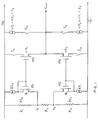
- the invention provides an output buffer of an integrated circuit arranged to be energised from a supply source providing predetermined potentials to supply conductors of said integrated circuit, the buffer comprising a potential divider, arranged to be supplied by the predetermined potentials and to define first and second reference potentials at first and second nodes, respectively, intermediate the predetermined potentials and thus defining a reduced voltage swing, a first pair of field effect semiconductor devices, the control electrodes of which are coupled together, and an electrode of one device being connected to the first node and the corresponding electrode of the other device of the pair being connected to an output node, a second pair of field effect semiconductor devices, the control electrodes of which are coupled together, and an electrode of one device being connected to the second node and the corresponding electrode of the other device of the pair also being connected to the output node, the dimensions of the channel of each semiconductor device that is connected to the output node being related to the dimensions of the channel of the other device of the respective pair, and the first and second pair being alternately energisable to permit the transfer
- the buffer forms part of a CMOS integrated circuit within a frequency synthesizer (not shown) used in the r.f circuit of a mobile telephone.
- the frequency synthesizer includes a phase lock loop which includes a pre-scaler which uses bipolar transistors and which varies the divide-by ratio in the phase lock loop.
- the divide-by ratio (or modulus) of the pre-scaler is varied between two fixed values by a modulus control output on the CMOS integrated circuit.
- the reference levels for the CMOS i.c. are a five volt logic swing and the modulus control output buffer provides a reduced logic swing of between 0.6 volts peak to peak and 1.1 volts peak to peak.
- a potential divider comprises resistors R 1 , R 2 , R 3 which is connected between rails V DD of 5 volts and 0 volts, the CMOS voltage reference levels.
- the potential divider defines, in conjunction with a pair of first current sources I 1 , I 2 , first and second reference potentials V, V, at first and second nodes, respectively, which potentials are intermediate the potentials V DD and 0.
- V DD (R 1 + R 3 )I 3 + (I 1 + I 3 )R 2
- V 1 V DD - R 1 I 3
- V 2 R 3 I 3
- the output node V out is required to rapidly charge and discharge capacitance associated with the modulus control input of the pre-sealer, (namely, the output capacitance of the buffer, the input capacitance of the pre-scaler plus stray capacitance such as board wiring) and the potential divider lacks the current capacity to do this.
- the reference potentials V 1 and V 2 are transferred to the output node V out by, respectively, a first pair of FETs M1, M2 of nmos conductivity type and a second pair of FETs M3, M4 of pmos conductivity type.
- the FETs M1, M3 are connected as diodes since the gates are connected to the respective drains, and are biased on, above the threshold voltage V t by respective current generators I 2 , I 1 .
- the gates of each pair of FETs are connected together, and it is envisaged that the gate source voltage V gs of the FETs of each pair are the same, to enable voltages V 1 , V 2 to be alternately transferred to node V out .
- I DS K(V gs - V t ) 2 , where V gs is the voltage between the gate and source of the FET and V t is the threshold voltage.
- K is a constant which depends on the aspect ratio of the channel, W/L, i.e. the ratio of the width to the length of the channel of the FET.
- V gs for M2 becomes greater than V gs for M1.
- a large current flows through M2 and the difference between this current and nI 2 flows through V out to the modulus control output.
- the capacitance associated with that node is rapidly charged, so that V gs reduces and the current through M2 reduces.
- V gs of M2 is equal to that for M1 and the current through M2 is equal to nI 2 .
- the peak current available at V out is typically approximately 50 mA.
- the circuit was designed to operate at 15 MHz with an input to output delay of 8 ns.
- the switchable current sources on the output node are required to accurately define the output voltage, to prevent the output devices entering the sub-threshold region and to define the output impedance.
- the circuit may also be operated without the switchable current sources but with reduced performance resulting specially in a much higher output impedance.
- the aspect ratio of M2 could be the same as that of M1, and n could equal unity for the current generator nI 2 (and the same for M4, M3 and nI 1 ). While the current available for switching would be much smaller, the potential of the output node would be unaffected by its loading.
- Resistors R 3 and R 4 together with current sources I 1 and I 2 define the upper and lower levels for the output voltage swing.
- V 1 -V 2 2 I 1 R 3 .
- the output swing is symmetrical around mid-supply. V 1 and V 2 are transferred to the output in the same way as that described above for the circuit of Figure 1, and the modifications described for Figure 1 are also applicable.
- the accuracy of the generated output voltages will depend on the matching accuracy of resistors R 1 , R 2 and R 3 , R 4 together with the matching accuracy of current sources I 1 , I 2 together with the absolute tolerance on R 3 , R 4 and I 1 , I 2 .
- nI 1 , nI 2 may be duplicated in order to provide a second output node V out ' at which antiphase voltages to that appearing at V out are present, i.e. a differential output buffer.
- the outputs V out and V out ' may be completely independent, i.e. a dual output buffer.
- the current sources I 1 , I 2 , nI 1 , nI 2 may all be slaved to a master reference current generator formed by a FET and a resistor to the power supply.
- I 1 , I 2 , nI 1 , nI 2 may be produced from a stable reference voltage such as a band gap reference voltage which is forced across a resistor R ref to generate a current I ref .
- I 1 , I 2 , nI 1 and nI 2 are then proportional to I ref .
- All resistors are fabricated using the same resistor material so that the output voltage swing V 1 - V 2 is independent of sheet resistivity.
- I 1 and I 2 also nI 1 , nI 2
- Decoupling capacitors may be employed between the gates of M1 and M3 and the respective supply rails in order to reduce voltage transients due to charge coupling between the outputs and a relatively high impedance bias circuit.
- Means may be provided where the output buffer may become tristate when a standby input becomes active so that all current sources are turned off.
Landscapes
- Engineering & Computer Science (AREA)
- Computer Hardware Design (AREA)
- Physics & Mathematics (AREA)
- Computing Systems (AREA)
- General Engineering & Computer Science (AREA)
- Mathematical Physics (AREA)
- Logic Circuits (AREA)
- Supply And Distribution Of Alternating Current (AREA)
- Direct Current Feeding And Distribution (AREA)
Applications Claiming Priority (2)
| Application Number | Priority Date | Filing Date | Title |
|---|---|---|---|
| GB9524957A GB2308027B (en) | 1995-12-06 | 1995-12-06 | Integrated circuit output buffer |
| GB9524957 | 1995-12-06 |
Publications (2)
| Publication Number | Publication Date |
|---|---|
| EP0778672A2 true EP0778672A2 (fr) | 1997-06-11 |
| EP0778672A3 EP0778672A3 (fr) | 1998-10-21 |
Family
ID=10785009
Family Applications (1)
| Application Number | Title | Priority Date | Filing Date |
|---|---|---|---|
| EP96308304A Withdrawn EP0778672A3 (fr) | 1995-12-06 | 1996-11-15 | Tampon de sortie en circuit intégré |
Country Status (4)
| Country | Link |
|---|---|
| US (1) | US5982207A (fr) |
| EP (1) | EP0778672A3 (fr) |
| JP (1) | JP3884805B2 (fr) |
| GB (1) | GB2308027B (fr) |
Families Citing this family (5)
| Publication number | Priority date | Publication date | Assignee | Title |
|---|---|---|---|---|
| US6154075A (en) * | 1999-05-18 | 2000-11-28 | Level One Communications, Inc. | Error correcting programmable pulse generator |
| KR100412134B1 (ko) * | 2001-06-27 | 2003-12-31 | 주식회사 하이닉스반도체 | 넓은 범위의 전원전압에서 동작하는 데이터 출력 버퍼 및이를 이용하는 반도체 메모리 장치 |
| US6605982B2 (en) * | 2001-06-29 | 2003-08-12 | Stmicroelectronics Inc. | Bias circuit for a transistor of a storage cell |
| JP3666423B2 (ja) * | 2001-07-06 | 2005-06-29 | 日本電気株式会社 | 駆動回路 |
| US20100102873A1 (en) * | 2008-10-23 | 2010-04-29 | Chen-Yu Huang | Output Driving Circuit for an Ethernet Transceiver |
Family Cites Families (11)
| Publication number | Priority date | Publication date | Assignee | Title |
|---|---|---|---|---|
| US4573177A (en) * | 1984-02-06 | 1986-02-25 | The United States Of America As Represented By The Secretary Of The Air Force | Bi-directional current differencer for complementary charge coupled device (CCD) outputs |
| JPS6350209A (ja) * | 1986-08-20 | 1988-03-03 | Matsushita Electric Ind Co Ltd | レベルシフト回路 |
| US4791326A (en) * | 1987-01-22 | 1988-12-13 | Intel Corporation | Current controlled solid state switch |
| US5105102A (en) * | 1990-02-28 | 1992-04-14 | Nec Corporation | Output buffer circuit |
| JPH04127703A (ja) * | 1990-09-19 | 1992-04-28 | Sony Corp | 演算増幅回路 |
| US5089723A (en) * | 1990-11-15 | 1992-02-18 | National Semiconductor Corporation | CMOS-based pseudo ECL output buffer |
| DE59109062D1 (de) * | 1991-04-16 | 1998-11-12 | Siemens Ag | Ausgangspufferverstärker mit grossem Signalhub |
| US5351012A (en) * | 1993-04-02 | 1994-09-27 | Elantec, Inc. | Low input resistance current-mode feedback operational amplifier input stage |
| US5517148A (en) * | 1994-10-31 | 1996-05-14 | Sgs-Thomson Microelectronics, Inc. | Low current differential level shifter |
| JP3033673B2 (ja) * | 1995-04-21 | 2000-04-17 | 日本電気株式会社 | 電力増幅用の演算増幅回路 |
| US5559476A (en) * | 1995-05-31 | 1996-09-24 | Cirrus Logic, Inc. | Voltage controlled oscillator including voltage controlled delay circuit with power supply noise isolation |
-
1995
- 1995-12-06 GB GB9524957A patent/GB2308027B/en not_active Expired - Fee Related
-
1996
- 1996-11-15 EP EP96308304A patent/EP0778672A3/fr not_active Withdrawn
- 1996-11-25 US US08/755,985 patent/US5982207A/en not_active Expired - Lifetime
- 1996-12-05 JP JP34049796A patent/JP3884805B2/ja not_active Expired - Lifetime
Non-Patent Citations (1)
| Title |
|---|
| None |
Also Published As
| Publication number | Publication date |
|---|---|
| JPH09191578A (ja) | 1997-07-22 |
| GB2308027A (en) | 1997-06-11 |
| GB2308027B (en) | 2000-05-10 |
| EP0778672A3 (fr) | 1998-10-21 |
| JP3884805B2 (ja) | 2007-02-21 |
| GB9524957D0 (en) | 1996-02-07 |
| US5982207A (en) | 1999-11-09 |
Similar Documents
| Publication | Publication Date | Title |
|---|---|---|
| KR100288818B1 (ko) | 반도체 집적회로 | |
| US3631528A (en) | Low-power consumption complementary driver and complementary bipolar buffer circuits | |
| US7800405B2 (en) | Passgate structures for use in low-voltage applications | |
| US7443200B2 (en) | Capacitor-coupled level shifter with duty-cycle independence and supply referenced bias configuration | |
| EP0202074A1 (fr) | Circuit générateur de polarisation | |
| US5469116A (en) | Clock generator circuit with low current frequency divider | |
| US5886556A (en) | Low power schmitt trigger | |
| US5162674A (en) | Current-steering CMOS logic family | |
| US6181166B1 (en) | Tristate driver for integrated circuit interconnects | |
| KR0162929B1 (ko) | 디지탈 신호 처리용 지연 회로 | |
| US6724268B2 (en) | Variable delay circuit, and differential voltage-controlled ring oscillator using the same, and PLL using the oscillator | |
| EP0361529B1 (fr) | Oscillateur commandé en tension | |
| US5774007A (en) | Clock distributing apparatus having V/I and I/V converters | |
| US5550503A (en) | Circuits and method for reducing voltage error when charging and discharging a capacitor through a transmission gate | |
| US5621360A (en) | Voltage supply isolation buffer | |
| KR100214548B1 (ko) | 전압 제어발진기 | |
| EP0156560A1 (fr) | Circuit CMOS comme détecteur de niveau correct de tension d'alimentation | |
| EP0778672A2 (fr) | Tampon de sortie en circuit intégré | |
| KR101291522B1 (ko) | 다중 게이트 트랜지스터를 갖는 전압 제어 발진기 및 그방법 | |
| US4383224A (en) | NMOS Crystal oscillator | |
| KR960702698A (ko) | 전자 회로(CMOS input with Vcc compensated dynamic threshold) | |
| KR940003448A (ko) | 반도체 기억장치 | |
| US6867629B2 (en) | Integrated circuit and method of adjusting capacitance of a node of an integrated circuit | |
| US7256657B2 (en) | Voltage controlled oscillator having digitally controlled phase adjustment and method therefor | |
| KR100468068B1 (ko) | 스티프 에지를 가지는 지연 스테이지 |
Legal Events
| Date | Code | Title | Description |
|---|---|---|---|
| PUAI | Public reference made under article 153(3) epc to a published international application that has entered the european phase |
Free format text: ORIGINAL CODE: 0009012 |
|
| AK | Designated contracting states |
Kind code of ref document: A2 Designated state(s): AT DE ES FR GB IT |
|
| PUAL | Search report despatched |
Free format text: ORIGINAL CODE: 0009013 |
|
| RAP1 | Party data changed (applicant data changed or rights of an application transferred) |
Owner name: MITEL SEMICONDUCTOR LIMITED |
|
| AK | Designated contracting states |
Kind code of ref document: A3 Designated state(s): AT DE ES FR GB IT |
|
| STAA | Information on the status of an ep patent application or granted ep patent |
Free format text: STATUS: THE APPLICATION IS DEEMED TO BE WITHDRAWN |
|
| 18D | Application deemed to be withdrawn |
Effective date: 19990422 |