EP0780030B1 - Diode laser de grande puissance - Google Patents
Diode laser de grande puissance Download PDFInfo
- Publication number
- EP0780030B1 EP0780030B1 EP95928043A EP95928043A EP0780030B1 EP 0780030 B1 EP0780030 B1 EP 0780030B1 EP 95928043 A EP95928043 A EP 95928043A EP 95928043 A EP95928043 A EP 95928043A EP 0780030 B1 EP0780030 B1 EP 0780030B1
- Authority
- EP
- European Patent Office
- Prior art keywords
- region
- balance
- refractive index
- active region
- confinement
- Prior art date
- Legal status (The legal status is an assumption and is not a legal conclusion. Google has not performed a legal analysis and makes no representation as to the accuracy of the status listed.)
- Expired - Lifetime
Links
Images


Classifications
-
- H—ELECTRICITY
- H01—ELECTRIC ELEMENTS
- H01S—DEVICES USING THE PROCESS OF LIGHT AMPLIFICATION BY STIMULATED EMISSION OF RADIATION [LASER] TO AMPLIFY OR GENERATE LIGHT; DEVICES USING STIMULATED EMISSION OF ELECTROMAGNETIC RADIATION IN WAVE RANGES OTHER THAN OPTICAL
- H01S5/00—Semiconductor lasers
- H01S5/20—Structure or shape of the semiconductor body to guide the optical wave ; Confining structures perpendicular to the optical axis, e.g. index or gain guiding, stripe geometry, broad area lasers, gain tailoring, transverse or lateral reflectors, special cladding structures, MQW barrier reflection layers
-
- H—ELECTRICITY
- H01—ELECTRIC ELEMENTS
- H01S—DEVICES USING THE PROCESS OF LIGHT AMPLIFICATION BY STIMULATED EMISSION OF RADIATION [LASER] TO AMPLIFY OR GENERATE LIGHT; DEVICES USING STIMULATED EMISSION OF ELECTROMAGNETIC RADIATION IN WAVE RANGES OTHER THAN OPTICAL
- H01S5/00—Semiconductor lasers
- H01S5/20—Structure or shape of the semiconductor body to guide the optical wave ; Confining structures perpendicular to the optical axis, e.g. index or gain guiding, stripe geometry, broad area lasers, gain tailoring, transverse or lateral reflectors, special cladding structures, MQW barrier reflection layers
- H01S5/2004—Confining in the direction perpendicular to the layer structure
-
- H—ELECTRICITY
- H01—ELECTRIC ELEMENTS
- H01S—DEVICES USING THE PROCESS OF LIGHT AMPLIFICATION BY STIMULATED EMISSION OF RADIATION [LASER] TO AMPLIFY OR GENERATE LIGHT; DEVICES USING STIMULATED EMISSION OF ELECTROMAGNETIC RADIATION IN WAVE RANGES OTHER THAN OPTICAL
- H01S5/00—Semiconductor lasers
- H01S5/20—Structure or shape of the semiconductor body to guide the optical wave ; Confining structures perpendicular to the optical axis, e.g. index or gain guiding, stripe geometry, broad area lasers, gain tailoring, transverse or lateral reflectors, special cladding structures, MQW barrier reflection layers
- H01S5/2004—Confining in the direction perpendicular to the layer structure
- H01S5/2009—Confining in the direction perpendicular to the layer structure by using electron barrier layers
-
- H—ELECTRICITY
- H01—ELECTRIC ELEMENTS
- H01S—DEVICES USING THE PROCESS OF LIGHT AMPLIFICATION BY STIMULATED EMISSION OF RADIATION [LASER] TO AMPLIFY OR GENERATE LIGHT; DEVICES USING STIMULATED EMISSION OF ELECTROMAGNETIC RADIATION IN WAVE RANGES OTHER THAN OPTICAL
- H01S5/00—Semiconductor lasers
- H01S5/20—Structure or shape of the semiconductor body to guide the optical wave ; Confining structures perpendicular to the optical axis, e.g. index or gain guiding, stripe geometry, broad area lasers, gain tailoring, transverse or lateral reflectors, special cladding structures, MQW barrier reflection layers
- H01S5/2004—Confining in the direction perpendicular to the layer structure
- H01S5/2018—Optical confinement, e.g. absorbing-, reflecting- or waveguide-layers
- H01S5/2031—Optical confinement, e.g. absorbing-, reflecting- or waveguide-layers characterized by special waveguide layers, e.g. asymmetric waveguide layers or defined bandgap discontinuities
-
- H—ELECTRICITY
- H01—ELECTRIC ELEMENTS
- H01S—DEVICES USING THE PROCESS OF LIGHT AMPLIFICATION BY STIMULATED EMISSION OF RADIATION [LASER] TO AMPLIFY OR GENERATE LIGHT; DEVICES USING STIMULATED EMISSION OF ELECTROMAGNETIC RADIATION IN WAVE RANGES OTHER THAN OPTICAL
- H01S5/00—Semiconductor lasers
- H01S5/20—Structure or shape of the semiconductor body to guide the optical wave ; Confining structures perpendicular to the optical axis, e.g. index or gain guiding, stripe geometry, broad area lasers, gain tailoring, transverse or lateral reflectors, special cladding structures, MQW barrier reflection layers
- H01S5/22—Structure or shape of the semiconductor body to guide the optical wave ; Confining structures perpendicular to the optical axis, e.g. index or gain guiding, stripe geometry, broad area lasers, gain tailoring, transverse or lateral reflectors, special cladding structures, MQW barrier reflection layers having a ridge or stripe structure
- H01S5/227—Buried mesa structure ; Striped active layer
- H01S5/2275—Buried mesa structure ; Striped active layer mesa created by etching
Definitions
- the invention describes a high power laser diode with potential use in ophthalmology, surgery, printing, magneto-optical data storage.
- the problem solved by this invention is the designing of a laser diode structure made of multiple layers which operates with a low value of the confinement factor less, than 0.015, and which has the thickness of the active region greater than 0.01 ⁇ m and small values for the confinement factor of the small energy gap layers, others than the active region.
- the high power laser diodes according to the invention present the following advantages:
- the high power laser diode structure according to the invention consists of the following regions: a substrate 1 , an n-type confinement region 2 , a p-type confinement region 3 , a passive region 4 , situated between the two named confinement regions and which constitutes the main part of the wave guide, an active region 5 , situated inside the wave guide and closer to the p-type confinement region, a balance region 6 which equilibrates the active region influence, situated inside the wave guide at the separation limit between the passive region and the n-type confinement region, a contact layer 7 , a p-type metallic contact 8 , and a n-type metallic contact 9 .
- the passive region is divided into two parts: a part 4 , between the balance region 6 and the active region 5 , and a part 4 ', between the active region 5 and the p-type confinement region 3 .
- the regions interfaces are parallel to each other and also parallel with the plane yOz, and the laser radiation is propagating in the Oz direction.
- the laser radiation is produced in the active region by the injection of the minority carriers in a p-n junction situated inside or in the neighborhood of the active region.
- the injection current is produced by applying a positive bias between the two metallic contacts 8 and 9 .
- the refraction index varies in the Ox direction.
- the refraction indexes for the regions 1 ... 7 have correspondingly the symbols n 1 ... n 7 .
- the profile of the refractive index along the Ox direction for a typical structure is presented in fig. 2.
- the field distribution in this structure in presented in fig. 3.
- the profile ofthe energy band gap of the regions along the Ox direction is presented in fig. 4.
- the refractive index profile has two bumps: a bump 10 corresponding to active region and a bump 11 corresponding to the balance region.
- the active region 5 is situated near the p-type confinement layer 3
- the balance region 6 is situated at the separation limit between the passive region 4 and n-type confinement region 2 .
- the thickness of the active region and of the balance region are d 5 and d 6 , respectively, and the thickness of the passive region including d 5 and d 6 , is d 4 .
- the distances between the balance region and the active region, and between the active region and the p-type confinement region, are I 4 and I' 4 , respectively.
- the refractive index of the active region n 5 has the highest value. This high value is a consequence of a low value of the energy band gap of the active region.
- the energy band gap of the passive region is higher, in order to obtain an efficient carrier confinement inside the active region.
- the refractive index in the passive region n 4 is lower than n 5 .
- the difference of the refractive indexes ( n 5 - n 4 ) determines, together with the effective thickness of the active region d 5 , the magnitude of a bump in the refractive index profile, magnitude equal to: d 5 (n 5 2 - n 4 2 ) 1/2
- the magnitude of the bump of the active region must be lower than ⁇ /4, i.e. the following condition has to be fulfilled: d 5 (n 5 2 - n 4 2 ) 1/2 ⁇ ⁇ /4
- the lowest value of the refractive index is that of the p-type confinement region, n 3 .
- the next higher value is that of the refractive index of the passive region n 4 , then that of the refractive index of the n-type confinement region, n 2 .
- a high, difference between n 4 and n 3 induces the repelling of the optical field toward the n-type confinement region.
- the balance region 6 has the role to attract toward it the maximum of the optical field distribution, thus reducing the value of the confinement factor.
- the refractive index of this region, n 6 . is higher than the refractive index of the adjacent regions: the passive region and the n-type confinement region.
- the attraction of the optical field toward the bump of the balance region is enhanced by the repelling of the optical field due to the existence of a high variation of the refractive index at the limit between the passive region and p-type confinement region.
- the magnitude of the its bump must be as high as possible, i.e. the difference n 6 - n 2 must be as high as possible.
- n 6 can not be very close to n 5 because this would determine the energy band gap of the active region and the balance region to be also very close and this would induce the balance region absorption of the radiation emitted in the active region.
- the efficiency of the bump of the balance region is direct proportional with its magnitude, the magnitude of the bump of the balance region must not be very close to the ⁇ /4 value, since in this case the optical field would be captured entirely inside the balance region. ⁇ 6 would become almost unity, and the two photons absorption processes in a region with a relative narrow energy band gap would be predominant compared with the other absorption processes.
- the higher order modes are cutt off by imposing the conditions that the refractive index of the n-type confinement region is higher or equal then the refractive index of the passive region and that the two bump magnitudes are lower than ⁇ /4.
- a small (positive) difference between the refractive index of the n-type confinement region and the refractive index of the passive region should be used, especially in the case when the two bumps, both of high magnitude, are far from one another.
- the thickness of the balance region was chosen to be 100 nm.
- the values chosen as examples for the confinement factor are 0.0144, 0.0072, 0.0036, 0.0018.
- the values chosen as examples for the thickness of the active region are 10 nm, 20 nm, 40 nm and 80 nm.
- the case for the 10 nm active region thickness wood need some correction for the values of the refractive indexes of the structure corresponding to the quantum well effects. This corrections are not essential for the demonstration and are not taken into account.
- the increase in the composition index of the p-type confinement region is determined by the necessity of an, as efficient as possible, repelling action of the optical field from the p-type confinement region.
- the examples shall be given for a active region made up of a single 'thick' layer. Small differences may appear if a few quantum-wells replace a single equivalent 'thick' layer. No.
- composition index of the active region is 0.11 and the wavelength of the emitted light is close to 800 nm.
- the composition indexes for regions 4 , 5 , 6 are: 0.35, 0.11 and 0.21, respectively, and the composition indexes for the p-type confinement region are 0.35, 0.40, 0.48 and 0.60 for active region thickness of 10 nm, 20 nm, 40 nm and 80 nm, respectively.
- the composition index in the n-type confinement layer 2 is given in the table for each case separately.
- the refractive index in the n-type confinement region step up compared to the refractive index of the passive region will be exploited, to cut-off the higher order modes in structures with the thickest active region
- An other extension of the invention refers to the number of balance regions. Beside the balance region 6 at the limit of the passive region 4 and the n-type confinement region 2 , one or more secondary balance regions, 6' , 6" etc. can be introduced between the balance region 6 and the active region 5 , with the value of the bumps 11' , 11" etc. also lower than ⁇ /4.
- the composition indexes for the p-type confinement region 3 , the passive region 4 the active region 5 , the secondary balance region 6' , the main balance region 6 and the n-type confinement region 2 are: 0.6, 0.35, 0.0, 0.15, 0.15 and 0.32, respectively.
- the thickness of the active region 5 , the secondary balance region 6' and the main balance region 6 are 80 nm, 60 nm and 80 nm respectively.
- the active region is placed at the limit between the p-type confinement region 3 and the passive region 4 .
- the distance between the active region 5 and the secondary balance region 6' and the distance between the secondary balance region 6' and the main balance region 6 are both equal to 0.6 ⁇ m.
- This structure has a confinement factor of 1.87 ⁇ 10 3 .
- the refractive index profile of this structure is presented in fig.5.
- the optical field distribution for this structure is presented in fig. 6.
- the above described structures can be obtained by epitaxyally growth, with thin layers, parallel each another and to the growth substrate. Stripes with a width w of several microns are defined from these structures by various methods. The demarcation of the stripes has two purposes:
- a very common used method to define the stripes is the creation of a ridge, by partial etching of the p-type confinement regions and by the subsequent oxidation of the regions where the etching was performed.
- This ridge is covered by a metal contact and through it the electric current will flow.
- the thinning of the p-type confinement region produces a small decrease of the effective refractive index which is used for the (partial) confinement of the optical field.
- the disadvantage of this method resides in the fact that the active region is not removed outside the stripe and that its lateral regions that are not excited by the electric current are strongly absorbant, that enhances the modal attenuation coefficient.
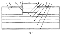
- a section through a stripe structure is presented, which derives from a dual planar structure, with two bumps of the refractive index profile in the Ox-direction of the materials which forms the planar structure.
- the stripe has a width w.
- the eptaxial structure contains all the regions described in fig.2.
- the epitaxial structure contains a i-type confinement region 12 and does not contain the active region 5 and the p-type confinement region 3 .
- the i-type regions 12 can consists of a semiconductor material, from the same material system as the rest of materials from which the stripe structure is made, and can be insulating from electrical point of view.
- the wave guide of width w is formed mainly around the bump of balance region, and is laterally bordered by wave guides formed mainly around the same bump of the balance region, not containing the active region.
- the refractive index of the regions 12 From the adjustment of the refractive index of the regions 12 one can obtain a fine tuning of the effective refractive indexes in the stripe wave guide and in the lateral wave guides, such that the variations of the elective refractive indexes to permit the operation in the lateral fundamental mode.
- the variation of the effective refractive indexes are equal to 0.0003, i.e. the optimum value for stripes of 12 ⁇ m width, which corresponds to the chosen confinement factor [1].
Landscapes
- Physics & Mathematics (AREA)
- Geometry (AREA)
- Condensed Matter Physics & Semiconductors (AREA)
- General Physics & Mathematics (AREA)
- Electromagnetism (AREA)
- Optics & Photonics (AREA)
- Semiconductor Lasers (AREA)
Claims (3)
- Diode laser haute puissance, possédant une structure constituée par :la structure étant telle que :une région de confinement de type p (3), qui présente la valeur d'indice de réfraction la plus basse au sein de la structure;une région passive (4) située entre les deux régions de confinement (2) et (3) et représentant la partie principale d'un guide d'ondes et dont l'indice de réfraction (n4) peut être abaissé graduellement ou en continu relativement à l'indice de réfraction de la région de confinement de type n (2), cette baisse étant supérieure vers la limite de séparation entre la région passive (4) et la région de confinement p (3);une région active (5) de faible épaisseur, avec une épaisseur effective d5 agencée soit asymétriquement dans la région passive (4, 4') et plus près de la région de confinement de type p (3), soit entre la région passive (4, 4') et la région de confinement de type p (3);une région d'équilibrage (6) de faible épaisseur, avec une épaisseur effective d6 se situant à la limite entre la région passive (4) et la région de confinement de type n (2), qui contrebalance l'influence de la région active (5), l'indice de réfraction de la région passive étant beaucoup plus élevé que l'indice de réfraction de ses régions voisines, à savoir la région passive (4) et la région de confinement de type n (2);le profil d'indice de réfraction présente deux tampons marqués, l'un correspondant à la région active (5), et l'autre à la région d'équilibrage (6), tous deux présentant une amplitude de d5 (n5 2-n4 2)1/2 respectivement d6 (n6 2-n4 2)1/2 inférieure à λ/4;la largeur de bande d'énergie interdite de la région d'équilibrage (6) est beaucoup plus grande que la largeur de bande d'énergie interdite de la région active (5), en vue d'éviter l'absorption, dans la région d'équilibrage (6), du rayonnement émis dans la région active;et, par l'action combinée de deux facteurs, l'attraction prédominante du champ par la région d'équilibrage (6) par comparaison à l'attraction de la région active (5) et la répulsion du champ due à l'échelon de l'indice de réfraction au niveau de la marge entre la région passive (4) et la région de confinement de type p (3) vers la région de confinement de type n (2), ladite structure de diode laser haute puissance assure :une répartition du champ ayant son maximum situé dans la région d'équilibrage (6), à l'extérieur du tampon de la région active (5), et une valeur réduite pour le facteur de confinement de la région active (5) par répulsion du maximum de répartition de champ hors de la région active (5), avecune réduction de la valeur du facteur de confinement de la région d'équilibrage (6) tenant à son épaisseur.
- Diode laser haute puissance selon la revendication 1, présentant une ou plusieurs régions d'équilibrage secondaires agencées entre la région active (5) et la région d'équilibrage principale (5).
- Diode laser haute puissance selon la revendication 1, présentant une structure zébrée et, de chaque côté de la zébrure, la structure épitaxiale contient une région de confinement de type i (12) et ne comprend pas la région active (5) ni la région de confinement de type p (3), ce qui fait que dans la zone zébrée, le guide d'onde à zébrure de largeur w est formé principalement autour du tampon de la région d'équilibrage et est limité, latéralement, par des guides d'ondes latéraux prévus principalement autour du même tampon de la région d'équilibrage mais ne contenant pas la région active.
Applications Claiming Priority (3)
| Application Number | Priority Date | Filing Date | Title |
|---|---|---|---|
| RO9401494 | 1994-09-09 | ||
| RO94-01494A RO109906B1 (ro) | 1994-09-09 | 1994-09-09 | Dioda laser, de mare putere |
| PCT/RO1995/000011 WO1996008062A1 (fr) | 1994-09-09 | 1995-08-18 | Diode laser de grande puissance |
Publications (2)
| Publication Number | Publication Date |
|---|---|
| EP0780030A1 EP0780030A1 (fr) | 1997-06-25 |
| EP0780030B1 true EP0780030B1 (fr) | 2000-05-17 |
Family
ID=20101081
Family Applications (1)
| Application Number | Title | Priority Date | Filing Date |
|---|---|---|---|
| EP95928043A Expired - Lifetime EP0780030B1 (fr) | 1994-09-09 | 1995-08-18 | Diode laser de grande puissance |
Country Status (5)
| Country | Link |
|---|---|
| US (1) | US6522677B1 (fr) |
| EP (1) | EP0780030B1 (fr) |
| DE (1) | DE69517039T2 (fr) |
| RO (1) | RO109906B1 (fr) |
| WO (1) | WO1996008062A1 (fr) |
Families Citing this family (20)
| Publication number | Priority date | Publication date | Assignee | Title |
|---|---|---|---|---|
| DE19717571A1 (de) * | 1997-04-25 | 1998-10-29 | Fraunhofer Ges Forschung | Diodenlaser-Oszillator oder- Verstärker mit wenigstens einer lichtleitenden Halbleiterschicht |
| US6167073A (en) * | 1998-07-23 | 2000-12-26 | Wisconsin Alumni Research Foundation | High power laterally antiguided semiconductor light source with reduced transverse optical confinement |
| DE10046580A1 (de) | 2000-09-20 | 2002-04-04 | Osram Opto Semiconductors Gmbh | Halbleiter-Laser |
| US6993053B2 (en) | 2002-04-03 | 2006-01-31 | The Australian National University | Thin clad diode laser |
| US7251381B2 (en) | 2002-04-03 | 2007-07-31 | The Australian National University | Single-mode optical device |
| AUPS150702A0 (en) | 2002-04-03 | 2002-05-09 | Australian National University, The | A low divergence diode laser |
| US6724795B2 (en) | 2002-05-10 | 2004-04-20 | Bookham Technology, Plc | Semiconductor laser |
| US20060001677A1 (en) * | 2003-11-06 | 2006-01-05 | Marc Webb | Color selection and coordination system |
| US7403552B2 (en) | 2006-03-10 | 2008-07-22 | Wisconsin Alumni Research Foundation | High efficiency intersubband semiconductor lasers |
| US7457338B2 (en) | 2006-04-19 | 2008-11-25 | Wisconsin Alumni Research Foundation | Quantum well lasers with strained quantum wells and dilute nitride barriers |
| EP2015412B1 (fr) * | 2007-07-06 | 2022-03-09 | Lumentum Operations LLC | Laser semiconducteur doté de divergence de faisceau étroite. |
| FI20085512A0 (fi) * | 2008-05-28 | 2008-05-28 | Oulun Yliopisto | Puolijohdelaser |
| US7830938B2 (en) * | 2008-12-15 | 2010-11-09 | Jds Uniphase Corporation | Laser diode |
| US9912118B2 (en) | 2010-06-28 | 2018-03-06 | Iulian Basarab Petrescu-Prahova | Diode laser type device |
| US9755402B2 (en) | 2010-06-28 | 2017-09-05 | Iulian Basarab Petrescu-Prahova | Edge emitter semiconductor laser type of device with end segments for mirrors protection |
| EP2741381B1 (fr) * | 2012-12-06 | 2020-05-06 | Nichia Corporation | Élément laser à semi-conducteur |
| WO2019002694A1 (fr) * | 2017-06-30 | 2019-01-03 | Oulun Yliopisto | Procédé de fabrication d'un appareil optique à semi-conducteurs et appareil |
| US20220190560A1 (en) * | 2020-12-15 | 2022-06-16 | Marvell Asia Pte, Ltd. | Gain medium structure for semiconductor optical amplifier with high saturation power |
| JP7778496B2 (ja) * | 2021-05-10 | 2025-12-02 | 日本ルメンタム株式会社 | 半導体レーザ |
| JP7793407B2 (ja) * | 2022-02-10 | 2026-01-05 | 古河電気工業株式会社 | 半導体レーザ素子 |
Family Cites Families (2)
| Publication number | Priority date | Publication date | Assignee | Title |
|---|---|---|---|---|
| NL184715C (nl) * | 1978-09-20 | 1989-10-02 | Hitachi Ltd | Halfgeleiderlaserinrichting. |
| RO102871B1 (en) * | 1990-04-20 | 1993-08-16 | Inst De Fizica Si Tehnologia M | High power laser diode |
-
1994
- 1994-09-09 RO RO94-01494A patent/RO109906B1/ro unknown
-
1995
- 1995-08-18 DE DE69517039T patent/DE69517039T2/de not_active Expired - Lifetime
- 1995-08-18 US US09/051,605 patent/US6522677B1/en not_active Expired - Fee Related
- 1995-08-18 WO PCT/RO1995/000011 patent/WO1996008062A1/fr not_active Ceased
- 1995-08-18 EP EP95928043A patent/EP0780030B1/fr not_active Expired - Lifetime
Also Published As
| Publication number | Publication date |
|---|---|
| RO109906B1 (ro) | 1995-06-30 |
| EP0780030A1 (fr) | 1997-06-25 |
| WO1996008062A1 (fr) | 1996-03-14 |
| US6522677B1 (en) | 2003-02-18 |
| DE69517039D1 (de) | 2000-06-21 |
| DE69517039T2 (de) | 2001-02-15 |
Similar Documents
| Publication | Publication Date | Title |
|---|---|---|
| EP0780030B1 (fr) | Diode laser de grande puissance | |
| US5701379A (en) | Waveguide type semiconductor photodetecting device and fabrication process therefor | |
| EP0602811B1 (fr) | Lasers à semi-conducteurs individuellement adressables, avec guides d'ondes integrés à faibles pertes | |
| US6455338B1 (en) | Method of manufacturing an integrated semiconductor laser-modulator device | |
| US5165105A (en) | Separate confinement electroabsorption modulator utilizing the Franz-Keldysh effect | |
| EP0437836A2 (fr) | Dispositif optique semi-conducteur | |
| US4360919A (en) | Semiconductor light emitting device | |
| KR100375275B1 (ko) | 다층반도체구조체및그제조방법 | |
| GB2111743A (en) | Semiconductor laser | |
| JPH10303500A (ja) | 高出力半導体レーザダイオード | |
| US6487225B2 (en) | Surface-emitting laser device | |
| US5008893A (en) | Tunable semiconductor laser | |
| US7405421B2 (en) | Optical integrated device | |
| EP0791967A1 (fr) | Photodetecteur du type a guide d'onde | |
| US5321714A (en) | Reflection suppression in semiconductor diode optical switching arrays | |
| US5763287A (en) | Method of fabricating semiconductor optical device | |
| US6724795B2 (en) | Semiconductor laser | |
| KR100569040B1 (ko) | 반도체 레이저 장치 | |
| US6272161B1 (en) | High power diode type laser devices | |
| EP1263099B1 (fr) | Laser à semi-conducteur | |
| EP0284684B1 (fr) | Laser à semi-conducteur avec canal inverse et substrat plan | |
| Mukai et al. | Laser beam scanning using a local deflector integrated with an effective mode filter | |
| CA2033246C (fr) | Dispositif optique a semiconducteur | |
| CN115280609B (zh) | 光学器件 | |
| JP3708758B2 (ja) | 半導体受光素子 |
Legal Events
| Date | Code | Title | Description |
|---|---|---|---|
| PUAI | Public reference made under article 153(3) epc to a published international application that has entered the european phase |
Free format text: ORIGINAL CODE: 0009012 |
|
| 17P | Request for examination filed |
Effective date: 19970408 |
|
| AK | Designated contracting states |
Kind code of ref document: A1 Designated state(s): BE CH DE FR GB IE IT LI NL SE |
|
| 17Q | First examination report despatched |
Effective date: 19971223 |
|
| GRAG | Despatch of communication of intention to grant |
Free format text: ORIGINAL CODE: EPIDOS AGRA |
|
| GRAG | Despatch of communication of intention to grant |
Free format text: ORIGINAL CODE: EPIDOS AGRA |
|
| GRAH | Despatch of communication of intention to grant a patent |
Free format text: ORIGINAL CODE: EPIDOS IGRA |
|
| GRAH | Despatch of communication of intention to grant a patent |
Free format text: ORIGINAL CODE: EPIDOS IGRA |
|
| GRAA | (expected) grant |
Free format text: ORIGINAL CODE: 0009210 |
|
| AK | Designated contracting states |
Kind code of ref document: B1 Designated state(s): BE CH DE FR GB IE IT LI NL SE |
|
| RIC1 | Information provided on ipc code assigned before grant |
Free format text: 7H 01S 5/30 A |
|
| REG | Reference to a national code |
Ref country code: IE Ref legal event code: FG4D Ref country code: CH Ref legal event code: EP |
|
| REF | Corresponds to: |
Ref document number: 69517039 Country of ref document: DE Date of ref document: 20000621 |
|
| ITF | It: translation for a ep patent filed | ||
| ET | Fr: translation filed | ||
| REG | Reference to a national code |
Ref country code: CH Ref legal event code: NV Representative=s name: KEMENY AG PATENTANWALTBUERO |
|
| PLBE | No opposition filed within time limit |
Free format text: ORIGINAL CODE: 0009261 |
|
| STAA | Information on the status of an ep patent application or granted ep patent |
Free format text: STATUS: NO OPPOSITION FILED WITHIN TIME LIMIT |
|
| 26N | No opposition filed | ||
| REG | Reference to a national code |
Ref country code: GB Ref legal event code: IF02 |
|
| REG | Reference to a national code |
Ref country code: CH Ref legal event code: PCAR Free format text: KEMENY AG PATENTANWALTBUERO;EISENGASSE 17;6004 LUZERN (CH) |
|
| PGFP | Annual fee paid to national office [announced via postgrant information from national office to epo] |
Ref country code: NL Payment date: 20100813 Year of fee payment: 16 Ref country code: IE Payment date: 20100820 Year of fee payment: 16 Ref country code: CH Payment date: 20100824 Year of fee payment: 16 |
|
| PGFP | Annual fee paid to national office [announced via postgrant information from national office to epo] |
Ref country code: SE Payment date: 20100812 Year of fee payment: 16 Ref country code: IT Payment date: 20100824 Year of fee payment: 16 Ref country code: FR Payment date: 20100901 Year of fee payment: 16 |
|
| PGFP | Annual fee paid to national office [announced via postgrant information from national office to epo] |
Ref country code: BE Payment date: 20100810 Year of fee payment: 16 |
|
| BERE | Be: lapsed |
Owner name: *PETRESCU-PRAHOVA IULIAN BASARAB Effective date: 20110831 Owner name: *VLAICU AUREL-MIHAI Effective date: 20110831 Owner name: *BUDA MANUELA Effective date: 20110831 |
|
| REG | Reference to a national code |
Ref country code: CH Ref legal event code: PFA Owner name: PETRESCU-PRAHOVA, IULIAN BASARAB Free format text: PETRESCU-PRAHOVA, IULIAN BASARAB#INSTITUTE OF PHYSICS AND TECHNOLOGY OF MATERIALS, P.O. BOX MG-7, MAGURELE#76900 BUCHAREST (RO) $ BUDA, MANUELA#INSTITUTE OF PHYSICS AND TECHNOLOGY OF MATERIALS, P.O. BOX MG-7, MAGURELE#76900 BUCHAREST (RO) $ VLAICU, AUREL-MIHAI#INSTITUTE OF PHYSICS AND TECHNOLOGY OF MATERIALS, P.O. BOX MG-7, MAGURELE#76900 BUCHAREST (RO) -TRANSFER TO- PETRESCU-PRAHOVA, IULIAN BASARAB#INSTITUTE OF PHYSICS AND TECHNOLOGY OF MATERIALS, P.O. BOX MG-7, MAGURELE#76900 BUCHAREST (RO) $ BUDA, MANUELA#INSTITUTE OF PHYSICS AND TECHNOLOGY OF MATERIALS, P.O. BOX MG-7, MAGURELE#76900 BUCHAREST (RO) $ VLAICU, AUREL-MIHAI#INSTITUTE OF PHYSICS AND TECHNOLOGY OF MATERIALS, P.O. BOX MG-7, |
|
| REG | Reference to a national code |
Ref country code: NL Ref legal event code: V1 Effective date: 20120301 |
|
| REG | Reference to a national code |
Ref country code: CH Ref legal event code: PL |
|
| REG | Reference to a national code |
Ref country code: SE Ref legal event code: EUG |
|
| PG25 | Lapsed in a contracting state [announced via postgrant information from national office to epo] |
Ref country code: CH Free format text: LAPSE BECAUSE OF NON-PAYMENT OF DUE FEES Effective date: 20110831 Ref country code: LI Free format text: LAPSE BECAUSE OF NON-PAYMENT OF DUE FEES Effective date: 20110831 |
|
| REG | Reference to a national code |
Ref country code: FR Ref legal event code: ST Effective date: 20120430 |
|
| REG | Reference to a national code |
Ref country code: IE Ref legal event code: MM4A |
|
| PG25 | Lapsed in a contracting state [announced via postgrant information from national office to epo] |
Ref country code: IT Free format text: LAPSE BECAUSE OF NON-PAYMENT OF DUE FEES Effective date: 20110818 Ref country code: NL Free format text: LAPSE BECAUSE OF NON-PAYMENT OF DUE FEES Effective date: 20120301 Ref country code: BE Free format text: LAPSE BECAUSE OF NON-PAYMENT OF DUE FEES Effective date: 20110831 |
|
| PGFP | Annual fee paid to national office [announced via postgrant information from national office to epo] |
Ref country code: DE Payment date: 20120206 Year of fee payment: 17 |
|
| PG25 | Lapsed in a contracting state [announced via postgrant information from national office to epo] |
Ref country code: IE Free format text: LAPSE BECAUSE OF NON-PAYMENT OF DUE FEES Effective date: 20110818 |
|
| PG25 | Lapsed in a contracting state [announced via postgrant information from national office to epo] |
Ref country code: FR Free format text: LAPSE BECAUSE OF NON-PAYMENT OF DUE FEES Effective date: 20110831 |
|
| PGFP | Annual fee paid to national office [announced via postgrant information from national office to epo] |
Ref country code: GB Payment date: 20120821 Year of fee payment: 18 |
|
| PG25 | Lapsed in a contracting state [announced via postgrant information from national office to epo] |
Ref country code: SE Free format text: LAPSE BECAUSE OF NON-PAYMENT OF DUE FEES Effective date: 20110819 |
|
| PG25 | Lapsed in a contracting state [announced via postgrant information from national office to epo] |
Ref country code: DE Free format text: LAPSE BECAUSE OF NON-PAYMENT OF DUE FEES Effective date: 20130301 |
|
| REG | Reference to a national code |
Ref country code: DE Ref legal event code: R119 Ref document number: 69517039 Country of ref document: DE Effective date: 20130301 |
|
| GBPC | Gb: european patent ceased through non-payment of renewal fee |
Effective date: 20130818 |
|
| PG25 | Lapsed in a contracting state [announced via postgrant information from national office to epo] |
Ref country code: GB Free format text: LAPSE BECAUSE OF NON-PAYMENT OF DUE FEES Effective date: 20130818 |