EP0782146A2 - Mémoire non volatile avec une zone de stockage de données et zone de données d'attributs pour stocker les données d'attributs de la zone de stockage de données - Google Patents
Mémoire non volatile avec une zone de stockage de données et zone de données d'attributs pour stocker les données d'attributs de la zone de stockage de données Download PDFInfo
- Publication number
- EP0782146A2 EP0782146A2 EP96120955A EP96120955A EP0782146A2 EP 0782146 A2 EP0782146 A2 EP 0782146A2 EP 96120955 A EP96120955 A EP 96120955A EP 96120955 A EP96120955 A EP 96120955A EP 0782146 A2 EP0782146 A2 EP 0782146A2
- Authority
- EP
- European Patent Office
- Prior art keywords
- memory
- data
- memory cells
- sector
- block
- Prior art date
- Legal status (The legal status is an assumption and is not a legal conclusion. Google has not performed a legal analysis and makes no representation as to the accuracy of the status listed.)
- Withdrawn
Links
- 230000004044 response Effects 0.000 claims 2
- 239000004065 semiconductor Substances 0.000 description 29
- 238000010586 diagram Methods 0.000 description 25
- 238000013500 data storage Methods 0.000 description 10
- 238000004519 manufacturing process Methods 0.000 description 9
- 238000004364 calculation method Methods 0.000 description 5
- 230000000694 effects Effects 0.000 description 5
- 101000685663 Homo sapiens Sodium/nucleoside cotransporter 1 Proteins 0.000 description 3
- 102100023116 Sodium/nucleoside cotransporter 1 Human genes 0.000 description 3
- ZMRUPTIKESYGQW-UHFFFAOYSA-N propranolol hydrochloride Chemical compound [H+].[Cl-].C1=CC=C2C(OCC(O)CNC(C)C)=CC=CC2=C1 ZMRUPTIKESYGQW-UHFFFAOYSA-N 0.000 description 3
- 230000003247 decreasing effect Effects 0.000 description 2
- 101001116774 Homo sapiens Methionine-R-sulfoxide reductase B2, mitochondrial Proteins 0.000 description 1
- 102100024862 Methionine-R-sulfoxide reductase B2, mitochondrial Human genes 0.000 description 1
- 101100467813 Saccharomyces cerevisiae (strain ATCC 204508 / S288c) RBS1 gene Proteins 0.000 description 1
- 230000032683 aging Effects 0.000 description 1
- 230000010485 coping Effects 0.000 description 1
- 239000011159 matrix material Substances 0.000 description 1
- 230000002035 prolonged effect Effects 0.000 description 1
- 230000001737 promoting effect Effects 0.000 description 1
Images


Classifications
-
- G—PHYSICS
- G11—INFORMATION STORAGE
- G11C—STATIC STORES
- G11C5/00—Details of stores covered by group G11C11/00
- G11C5/02—Disposition of storage elements, e.g. in the form of a matrix array
- G11C5/025—Geometric lay-out considerations of storage- and peripheral-blocks in a semiconductor storage device
-
- G—PHYSICS
- G11—INFORMATION STORAGE
- G11C—STATIC STORES
- G11C16/00—Erasable programmable read-only memories
-
- G—PHYSICS
- G11—INFORMATION STORAGE
- G11C—STATIC STORES
- G11C16/00—Erasable programmable read-only memories
- G11C16/02—Erasable programmable read-only memories electrically programmable
- G11C16/06—Auxiliary circuits, e.g. for writing into memory
- G11C16/22—Safety or protection circuits preventing unauthorised or accidental access to memory cells
Definitions
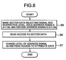
- According to the present invention includes at least one of sectors (sector is defined one word line) where sector data of a first byte number and attribute data of a second byte number corresponding to the sector data, are stored as one set of data in one row (column) or rows (columns) , are arranged, whereby an error correcting circuit in respect of data of one sector can be constituted by a circuit correcting error of one bit or bits. Therefore, a bit line failure and a memory cell failure can be relieved by the error correcting circuit whereby the manufacturing yield is promoted and the manufacturing cost can be reduced.
- a single sector can be arranged to rows of a small plural number as in the first embodiment.
- a 1 bit error correcting circuit may be constituted to relieve the initial failure of the single word line and the circuit scale can be rendered 1 several 10s-th of that in the conventional example.
- a number of rows (a number of columns) of one sector can significantly be decreased (minimum 1 row, 1 column) and the sector data and the attribute data can continuously be accessed thereby providing an effect by which the operational speed can be accelerated.
Landscapes
- Engineering & Computer Science (AREA)
- Microelectronics & Electronic Packaging (AREA)
- Computer Security & Cryptography (AREA)
- Read Only Memory (AREA)
- Techniques For Improving Reliability Of Storages (AREA)
- For Increasing The Reliability Of Semiconductor Memories (AREA)
Applications Claiming Priority (3)
| Application Number | Priority Date | Filing Date | Title |
|---|---|---|---|
| JP34151395A JP2848300B2 (ja) | 1995-12-27 | 1995-12-27 | 不揮発性半導体記憶装置 |
| JP34151395 | 1995-12-27 | ||
| JP341513/95 | 1995-12-27 |
Publications (2)
| Publication Number | Publication Date |
|---|---|
| EP0782146A2 true EP0782146A2 (fr) | 1997-07-02 |
| EP0782146A3 EP0782146A3 (fr) | 2003-07-16 |
Family
ID=18346650
Family Applications (1)
| Application Number | Title | Priority Date | Filing Date |
|---|---|---|---|
| EP96120955A Withdrawn EP0782146A3 (fr) | 1995-12-27 | 1996-12-27 | Mémoire non volatile avec une zone de stockage de données et zone de données d'attributs pour stocker les données d'attributs de la zone de stockage de données |
Country Status (4)
| Country | Link |
|---|---|
| US (1) | US5818754A (fr) |
| EP (1) | EP0782146A3 (fr) |
| JP (1) | JP2848300B2 (fr) |
| KR (1) | KR100273628B1 (fr) |
Cited By (1)
| Publication number | Priority date | Publication date | Assignee | Title |
|---|---|---|---|---|
| EP1708203A1 (fr) * | 2005-03-25 | 2006-10-04 | Samsung Electronics Co., Ltd. | Dispositif de mémoire non volatile et procédé de stockage d'informations d'état à l'aide de chaînes multiples |
Families Citing this family (9)
| Publication number | Priority date | Publication date | Assignee | Title |
|---|---|---|---|---|
| US7447069B1 (en) | 1989-04-13 | 2008-11-04 | Sandisk Corporation | Flash EEprom system |
| DE69024086T2 (de) * | 1989-04-13 | 1996-06-20 | Sundisk Corp | EEprom-System mit Blocklöschung |
| JP3411186B2 (ja) * | 1997-06-06 | 2003-05-26 | シャープ株式会社 | 不揮発性半導体記憶装置 |
| US6178532B1 (en) * | 1998-06-11 | 2001-01-23 | Micron Technology, Inc. | On-chip circuit and method for testing memory devices |
| US6148414A (en) * | 1998-09-24 | 2000-11-14 | Seek Systems, Inc. | Methods and systems for implementing shared disk array management functions |
| US7266706B2 (en) * | 1999-03-03 | 2007-09-04 | Yottayotta, Inc. | Methods and systems for implementing shared disk array management functions |
| US7061792B1 (en) * | 2002-08-10 | 2006-06-13 | National Semiconductor Corporation | Low AC power SRAM architecture |
| JPWO2007023544A1 (ja) | 2005-08-25 | 2009-03-26 | スパンション エルエルシー | 記憶装置、記憶装置の制御方法、および記憶制御装置の制御方法 |
| JP2008021390A (ja) * | 2006-07-14 | 2008-01-31 | Toshiba Corp | 半導体記憶装置 |
Citations (1)
| Publication number | Priority date | Publication date | Assignee | Title |
|---|---|---|---|---|
| JPH05189981A (ja) | 1992-01-10 | 1993-07-30 | Toshiba Corp | フラッシュ型eepromおよびそのフラッシュ型eepromを使用した電子計算機システム |
Family Cites Families (9)
| Publication number | Priority date | Publication date | Assignee | Title |
|---|---|---|---|---|
| US5268870A (en) * | 1988-06-08 | 1993-12-07 | Eliyahou Harari | Flash EEPROM system and intelligent programming and erasing methods therefor |
| JPH0748320B2 (ja) * | 1989-07-24 | 1995-05-24 | セイコー電子工業株式会社 | 半導体不揮発性メモリ |
| JPH03250499A (ja) * | 1990-02-27 | 1991-11-08 | Nec Corp | データ記憶回路 |
| JPH05151097A (ja) * | 1991-11-28 | 1993-06-18 | Fujitsu Ltd | 書換回数制限型メモリのデータ管理方式 |
| JP3251968B2 (ja) * | 1992-01-20 | 2002-01-28 | 富士通株式会社 | 半導体記憶装置 |
| ATA80592A (de) * | 1992-04-21 | 1995-06-15 | Vaillant Gmbh | Verfahren zum optimalen ausnutzen der speicherkapazität eines eeprom |
| JP2647312B2 (ja) * | 1992-09-11 | 1997-08-27 | インターナショナル・ビジネス・マシーンズ・コーポレイション | 一括消去型不揮発性半導体記憶装置 |
| US5388083A (en) * | 1993-03-26 | 1995-02-07 | Cirrus Logic, Inc. | Flash memory mass storage architecture |
| JPH08249895A (ja) * | 1995-03-10 | 1996-09-27 | Nec Corp | 不輝発性半導体記憶装置 |
-
1995
- 1995-12-27 JP JP34151395A patent/JP2848300B2/ja not_active Expired - Fee Related
-
1996
- 1996-12-27 EP EP96120955A patent/EP0782146A3/fr not_active Withdrawn
- 1996-12-27 US US08/773,900 patent/US5818754A/en not_active Expired - Lifetime
- 1996-12-27 KR KR1019960082417A patent/KR100273628B1/ko not_active Expired - Fee Related
Patent Citations (1)
| Publication number | Priority date | Publication date | Assignee | Title |
|---|---|---|---|---|
| JPH05189981A (ja) | 1992-01-10 | 1993-07-30 | Toshiba Corp | フラッシュ型eepromおよびそのフラッシュ型eepromを使用した電子計算機システム |
Cited By (2)
| Publication number | Priority date | Publication date | Assignee | Title |
|---|---|---|---|---|
| EP1708203A1 (fr) * | 2005-03-25 | 2006-10-04 | Samsung Electronics Co., Ltd. | Dispositif de mémoire non volatile et procédé de stockage d'informations d'état à l'aide de chaînes multiples |
| US7457911B2 (en) | 2005-03-25 | 2008-11-25 | Samsung Electronics Co., Ltd. | Nonvolatile memory device and method for storing status information using multiple strings |
Also Published As
| Publication number | Publication date |
|---|---|
| JP2848300B2 (ja) | 1999-01-20 |
| KR100273628B1 (ko) | 2001-01-15 |
| EP0782146A3 (fr) | 2003-07-16 |
| US5818754A (en) | 1998-10-06 |
| JPH09180485A (ja) | 1997-07-11 |
| KR970051327A (ko) | 1997-07-29 |
Similar Documents
| Publication | Publication Date | Title |
|---|---|---|
| US7403436B2 (en) | Non-volatile semiconductor memory device | |
| US5313425A (en) | Semiconductor memory device having an improved error correction capability | |
| US6314032B2 (en) | Semiconductor device with flexible redundancy system | |
| US7219271B2 (en) | Memory device and method for redundancy/self-repair | |
| US5524231A (en) | Nonvolatile memory card with an address table and an address translation logic for mapping out defective blocks within the memory card | |
| EP0660237B1 (fr) | Dispositif de mémoire à semi-conducteur à réseau de cellules de mémoire de réserve | |
| US7149135B2 (en) | Multi chip package type memory system and a replacement method of replacing a defect therein | |
| US20030126386A1 (en) | Memory system, method and predecoding circuit operable in different modes for selectively accessing multiple blocks of memory cells for simultaneous writing or erasure | |
| US5033024A (en) | Matrix memory with redundancy and minimizes delay | |
| US5818754A (en) | Nonvolatile memory having data storing area and attribute data area for storing attribute data of data storing area | |
| US6457093B2 (en) | Circuit and method to control operations of another circuit | |
| US8064258B2 (en) | Method apparatus, and system providing adjustable memory page configuration | |
| EP0153752B1 (fr) | Dispositif de mémoire à semi-conducteur comprenant une fonction de détection de bit d'erreur | |
| JPH07141478A (ja) | 受動ユニット計数集積回路 | |
| KR100305033B1 (ko) | 블럭 아키텍츄어 옵션 회로를 구비하는 불휘발성 반도체 메모리 장치 | |
| US6728136B2 (en) | Electronically rewritable non-volatile semiconductor memory device | |
| EP0428396A2 (fr) | Circuit de correction d'erreur de bit pour une mémoire non volatile | |
| JP3482543B2 (ja) | 半導体メモリ | |
| US6091641A (en) | Non-volatile memory device and method for the programming of the same | |
| US5226015A (en) | Semiconductor memory system | |
| KR100449269B1 (ko) | 고집적을 위한 불휘발성 반도체 메모리 장치 | |
| JPH0528779A (ja) | 不揮発性メモリ装置 | |
| JPH065082A (ja) | 半導体記憶装置 |
Legal Events
| Date | Code | Title | Description |
|---|---|---|---|
| PUAI | Public reference made under article 153(3) epc to a published international application that has entered the european phase |
Free format text: ORIGINAL CODE: 0009012 |
|
| AK | Designated contracting states |
Kind code of ref document: A2 Designated state(s): DE FR GB |
|
| RAP1 | Party data changed (applicant data changed or rights of an application transferred) |
Owner name: NEC ELECTRONICS CORPORATION |
|
| PUAL | Search report despatched |
Free format text: ORIGINAL CODE: 0009013 |
|
| AK | Designated contracting states |
Designated state(s): DE FR GB |
|
| RIC1 | Information provided on ipc code assigned before grant |
Ipc: 7G 11C 16/34 B Ipc: 7G 11C 16/06 B Ipc: 7G 11C 16/04 A |
|
| 17P | Request for examination filed |
Effective date: 20031120 |
|
| GRAP | Despatch of communication of intention to grant a patent |
Free format text: ORIGINAL CODE: EPIDOSNIGR1 |
|
| STAA | Information on the status of an ep patent application or granted ep patent |
Free format text: STATUS: THE APPLICATION IS DEEMED TO BE WITHDRAWN |
|
| 18D | Application deemed to be withdrawn |
Effective date: 20041210 |