EP0783159A2 - Synchronisierung für drahtlosen Sender - Google Patents
Synchronisierung für drahtlosen Sender Download PDFInfo
- Publication number
- EP0783159A2 EP0783159A2 EP97100050A EP97100050A EP0783159A2 EP 0783159 A2 EP0783159 A2 EP 0783159A2 EP 97100050 A EP97100050 A EP 97100050A EP 97100050 A EP97100050 A EP 97100050A EP 0783159 A2 EP0783159 A2 EP 0783159A2
- Authority
- EP
- European Patent Office
- Prior art keywords
- module
- slave
- pick
- antenna
- coil
- Prior art date
- Legal status (The legal status is an assumption and is not a legal conclusion. Google has not performed a legal analysis and makes no representation as to the accuracy of the status listed.)
- Granted
Links
Images

Classifications
-
- G—PHYSICS
- G06—COMPUTING OR CALCULATING; COUNTING
- G06K—GRAPHICAL DATA READING; PRESENTATION OF DATA; RECORD CARRIERS; HANDLING RECORD CARRIERS
- G06K7/00—Methods or arrangements for sensing record carriers, e.g. for reading patterns
- G06K7/0008—General problems related to the reading of electronic memory record carriers, independent of its reading method, e.g. power transfer
Definitions
- This invention relates to synchronization of signals and, more specifically, to the synchronization of wireless transmit carrier phase and transmit burst signals from radio frequency (RF) reading modules in a multiple reading module-transponder system.
- RF radio frequency
- a multiple reading module-transponder system there are a plurality of reading modules (or reading units) geographically spaced and a plurality of transponders which communicate with the reading modules. Communication between a transponder and a reading module (or unit) is initiated by the reading module. Specifically, the reading module transmits a charge-up burst which powers the transponder and prompts the transponder to transmit information back to the reader module.
- a reading module-transponder system is well known in the art, and disclosed in, for example, U.S. Patent No. issued to 5,053,774 to Schuermann et al., which is hereby incorporated by reference in its entirety.
- the prior art solves this problem by synchronizing the transmit bursts from the reader unit to transmit simultaneously. This is done by retrofitting existing reading units with interfaces, designating one reading unit to be the master reading unit and the remaining units as slave units, and placing cables between the master reading unit and each slave unit.
- a master reading unit is operated from its internal crystal oscillator.
- the frequency signal from the oscillator is supplied to all the other slave units via cabling. Accordingly, all reading units are operated from one oscillator only and allows for synchronized transmit bursts from all the slave units simultaneously.
- transmit carrier phase synchronization is employed to avoid beat effects of charge-up field strength.
- this transmit carrier phase synchronization is accomplished by incurring the expense of placing potentially large lengths of cabling.
- the invention is a method and apparatus which eliminates the need for physical cabling, and yet provides transmit carrier phase synchronization while simultaneously avoiding the beat effect.
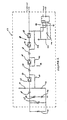
- the invention comprises a master RF module equipped with an antenna and internal oscillator, a slave RF module equipped with an antenna, oscillator input, and transmitter control, and additional circuitry which replaces a slave internal oscillator.
- a pick up coil disposed perpendicular to the antenna of master RF module, is connected to the additional circuitry. Transmission from the master RF module is received by the pick up coil and is filtered and amplified by the additional circuitry. The amplified signal is used as an oscillator input to the slave RF module and is also converted into a square wave monoflop signal for operating the transmitter control of the slave RF module.
- System 10 includes, in part, master radio frequency (RF) module 12 which comprises an internal oscillator 14, and antenna 16 connected to oscillator 14.
- RF radio frequency
- System 10 also includes, in part, slave RF module 20 which comprises an oscillator input 22, transmitter control 24, and antenna 26 which communicates with oscillator input 22 and transmitter control 24.
- slave RF module 20 which comprises an oscillator input 22, transmitter control 24, and antenna 26 which communicates with oscillator input 22 and transmitter control 24.
- System 10 further includes, in part, a pick up coil 30 disposed between master RF module 12 and slave RF module 20, and perpendicularly to both antenna 16 of master RF module 12, and to antenna 26 of slave RF module 20.
- Pick up coil 30 is shielded by aluminum shield 32 disposed between pick up coil 30 and antenna 26 of slave RF module 20.
- Aluminum shield 32 is oriented perpendicular to the field lines 34 generated by antenna 26 of slave RF module 20. Accordingly, aluminum shield 32 prevents feedback by an emerging charge-up burst oscillator signal emitted from antenna 26.
- an aluminum shield 36 may also be deployed between pick up coil 30 and master RF module 12 for similar reasons, although the present invention clearly contemplates that aluminum shield 36 may be omitted as required by the specific situation.
- shields 32 and 36 are made from aluminum. Although the aluminum material may perform best it is not necessarily the critical feature and thus it is clearly contemplated that for the aluminum there may be substituted any other material in various shapes or sizes which perform the similar function of shielding.
- Pick up coil 30 is connected to additional circuitry illustrated in a block diagram 40 in a dashed box.
- Block diagram 40 comprises filtering capacitor 42 in parallel with amplifier 44 connected in series to buffer/amplifier 46.
- the output from buffer/amplifier 46 is connected to both oscillator input 22 and a square wave converter 48.
- the output from square wave converter 48 is connected to transmitter control 24.
- system 10 (operating here at approximately 134.2 kHz) observes a beat effect on charge-up bursts when the master RF module 12 and slave RF module 20 are separated by a distance of approximately three meters or less.
- this distance will vary, depending on the operating frequency of system 10, e.g., lower frequencies observing a beat effect over longer distances, and depending on antenna size as is well-known in the art.
- the slave RF module 20 must match the frequency of the master RF module 12 and must also provide a stable phase relationship.
- the frequency of the master RF module 12 is fixed by internal oscillator 14.
- master RF module 12 transmits via antenna 16, as illustrated by field line 52, pick up coil 30 picks up the transmission.
- the transmission is then filtered by filtering capacitor 42, and amplified by amplifiers 44 and 46.
- the output of the amplifier is connected to oscillator input 22.
- slave RF module 20 will operate on the exact frequency as transmitted by master RF module 12 and thereby avoids any beat effect from being observed in system 10.
- oscillator input 22 operates from the same frequency as master RF module 12, a frequency match and a stable phase relationship are achieved, thereby avoiding the conditions which create a beat effect.
- a feature of the present embodiment is that transmitter control 24 enables transmission by the slave RF module 20 on and off.
- Square wave converter 48 converts the analog frequency transmission to a square wave signal monoflop signal which is then connected to transmitter control 24 of slave RF module 20.
- the monoflop signal enables transmitter control 24.
- square wave converter 48 produces a monoflop signal which enables transmission by slave RF module 20 via transmitter control 24.
- the period of such frequency is approximately 7.5 microseconds.
- the transmitter control 24 is set for a predetermined time period according to the frequency used by system 10. Based on the present 134.2 kHz system, the transmitter control 24 is set on a predetermined 10 microsecond period.
- a monoflop square wave signal should be generated at least every 7.5 microseconds which enables transmitter control 24 and allows slave RF module 20 to transmit.
- master RF module 12 ceases to transmit, no square wave signal is produced because the monoflop falls to its idle state.
- transmitter control 24 becomes non-enabled (disabled) and slave RF module 20 ceases to transmit.
- Shield 32 prevents transmissions from the antenna 26 of slave RF module 20 from being received by pick up coil 30. In doing so, shield 32 prevents an unstable feedback problem from developing. Similarly, shield 36 may be optionally employed if necessary to prevent any non-antenna 16 transmitted noise from degrading the signal received by pick up coil 30.
- the present invention enables a system 10 to employ multiple modules 12, 20, in close proximity without observing a beat effect on the charge-up field strengths by eliminating the constraint that cabling imposes and providing wireless transmit carrier phase synchronization.
- specific circuitry shown generally at 52, illustrated in a dashed box, may be used as a working example model of the general block diagram 40 shown in Figure 1. Accordingly, specific circuitry 52 is connected to pick up coil 30 having a value of 2.5 mH.
- Specific circuitry 52 comprises a capacitor (resonator) 54, voltage-clamping diodes 56 and 58, coupling capacitor 60, first amplifier shown generally at 64 which comprises simple CMOS inverter 66 and feedback resistor 68, voltage clamping diodes 70 and 72, coupling capacitor 74, second amplifier shown generally at 78 which comprises simple CMOS inverter 80 and feedback resistor 82, coupling capacitor 84, Schmitt trigger circuit shown generally at 88 which comprises first CMOS amplifier 90, second CMOS amplifier 92 and feedback resistor 94, square wave monoflop converter 98, resistor 104, and capacitor 106.
- oscillator signal pick up coil 30 receives the signal transmitted by master RF module 12 and is connected to capacitor 54, which filters the signal. It is noted that pick up coil 30 is disposed perpendicular to antenna 16 of master RF module 12 and between antenna 16 of master RF module 12 and antenna 26 of slave RF module 20. In addition, similar to the embodiment of Figure 1, shield 32 is disposed between the antenna 26 of slave RF module 20 and pick up coil 30.
- Capacitor 54 is adjustable, in order to set the resonance frequency to the pre-determined transmit frequency, in this case 134.2 kHz. However, it is clearly contemplated that a different pre-determined frequency may be used and capacitor 54 may be adjusted accordingly. In the present circuit, capacitor 54 is a 390 picofarad (pF) capacitor. Clearly, the specific values for pick up coil 30 and capacitor 54 are varied according to the frequency, and, even given a frequency, may be varied to according to the parts available.
- Diodes 56 and 58 are used to clamp excessive voltages which may occur when the pick up coil is placed too close to an antenna such as antenna 16 of master RF module 12. Any Zener diode with a Power rating of 0.25W can be used for either diode 56 or 58.
- Coupling capacitor 60 couples the received signal which has been filtered and cleared of too high voltages to first amplifier 64.
- Capacitor 60 comprises a 10 pF capacitor, although any capacitor value in the range from 5 pF to 100 pF may be used. However, it is important to note that capacitor 60 affects the resonance tuning of pick up coil 30 and capacitor 54.
- first amplifier 64 comprises a simple CMOS inverter 66 and feedback resistor 68 ranging from 1M to 10M.
- Diodes 70 and 72 are used to clamp excessive voltages, and any general purpose diode can be used.
- the output of amplifier 64 carrying amplified signal is then coupled via capacitor 74 to second amplifier 78.
- Any capacitor value can be used for capacitor 74 with the only limitation that it must be chosen consistent with the frequency range in use.
- Second amplifier 78 may range in value from 1M to 10M.
- Capacitor 84 (any appropriate coupling value, but limited by the frequency range in use) couples the output of second amplifier 78 to Schmitt trigger circuit 88.
- the output of Schmitt trigger circuit 88 which is the oscillator signal, is connected to oscillator input 22 shown in Figure 1.
- Resistor 82 of Schmitt trigger circuit 88 needs to range from 10k to 1M.
- the output of Schmitt trigger circuit 88 is also connected to square wave monoflop converter 98 which consists of a TTL circuit SN74LS123.
- the monoflop time constant is pre-determined by resistor 104 and capacitor 106, as is well-known in the art, and is set according to the frequency range in use. In the case of a system operating at 134.2 kHz, a time period of approximately 10 microseconds is set using a 33k resistor 104 and a 1NF capacitor 106.
- the output of square wave monoflop converter 98 is connected to and directly operates transmitter control 24 of slave RF module 20.
- the present invention would also encompass a system 10 which operates at a frequency other than 134.2 kHz with appropriate adjustments to the period of the transmitter control 24, the use of aluminum shield 32 and optional aluminum shield 36, and the various values of specific circuitry 52. While the various values of specific circuitry 52 may be adjusted based on the operation frequency and parts available, the changes will all be consistent with the intent of block diagram 40 of the present invention. Thus, the breadth and scope of the present invention should not be limited by any of the above-described exemplary embodiments, but should be defined only in accordance with the following claims appended hereto and their equivalents.
Landscapes
- Engineering & Computer Science (AREA)
- Artificial Intelligence (AREA)
- Computer Vision & Pattern Recognition (AREA)
- Physics & Mathematics (AREA)
- General Physics & Mathematics (AREA)
- Theoretical Computer Science (AREA)
- Near-Field Transmission Systems (AREA)
- Burglar Alarm Systems (AREA)
Applications Claiming Priority (2)
| Application Number | Priority Date | Filing Date | Title |
|---|---|---|---|
| US08/581,008 US5798709A (en) | 1996-01-03 | 1996-01-03 | Wireless transmitter carrier phase synchronization |
| US581008 | 1996-01-03 |
Publications (3)
| Publication Number | Publication Date |
|---|---|
| EP0783159A2 true EP0783159A2 (de) | 1997-07-09 |
| EP0783159A3 EP0783159A3 (de) | 1999-04-21 |
| EP0783159B1 EP0783159B1 (de) | 2002-10-09 |
Family
ID=24323525
Family Applications (1)
| Application Number | Title | Priority Date | Filing Date |
|---|---|---|---|
| EP97100050A Expired - Lifetime EP0783159B1 (de) | 1996-01-03 | 1997-01-03 | Synchronisierung für drahtlosen Sender |
Country Status (3)
| Country | Link |
|---|---|
| US (1) | US5798709A (de) |
| EP (1) | EP0783159B1 (de) |
| DE (1) | DE69716142T2 (de) |
Families Citing this family (60)
| Publication number | Priority date | Publication date | Assignee | Title |
|---|---|---|---|---|
| US7571139B1 (en) | 1999-02-19 | 2009-08-04 | Giordano Joseph A | System and method for processing financial transactions |
| US8538801B2 (en) | 1999-02-19 | 2013-09-17 | Exxonmobile Research & Engineering Company | System and method for processing financial transactions |
| US7837116B2 (en) | 1999-09-07 | 2010-11-23 | American Express Travel Related Services Company, Inc. | Transaction card |
| US7093767B2 (en) | 1999-09-07 | 2006-08-22 | American Express Travel Related Services Company, Inc. | System and method for manufacturing a punch-out RFID transaction device |
| US7156301B1 (en) | 1999-09-07 | 2007-01-02 | American Express Travel Related Services Company, Inc. | Foldable non-traditionally-sized RF transaction card system and method |
| US7070112B2 (en) | 1999-09-07 | 2006-07-04 | American Express Travel Related Services Company, Inc. | Transparent transaction device |
| US7239226B2 (en) | 2001-07-10 | 2007-07-03 | American Express Travel Related Services Company, Inc. | System and method for payment using radio frequency identification in contact and contactless transactions |
| US7306158B2 (en) | 2001-07-10 | 2007-12-11 | American Express Travel Related Services Company, Inc. | Clear contactless card |
| US7889052B2 (en) | 2001-07-10 | 2011-02-15 | Xatra Fund Mx, Llc | Authorizing payment subsequent to RF transactions |
| US6850468B2 (en) * | 1999-09-17 | 2005-02-01 | Seiko Epson Corporation | Electronic timepiece, control method for electronic timepiece, regulating system for electronic timepiece, and regulating method for electronic timepiece |
| US8429041B2 (en) | 2003-05-09 | 2013-04-23 | American Express Travel Related Services Company, Inc. | Systems and methods for managing account information lifecycles |
| US7268668B2 (en) | 2003-05-09 | 2007-09-11 | American Express Travel Related Services Company, Inc. | Systems and methods for managing multiple accounts on a RF transaction instrument |
| US8543423B2 (en) | 2002-07-16 | 2013-09-24 | American Express Travel Related Services Company, Inc. | Method and apparatus for enrolling with multiple transaction environments |
| US7172112B2 (en) | 2000-01-21 | 2007-02-06 | American Express Travel Related Services Company, Inc. | Public/private dual card system and method |
| WO2001067355A2 (en) | 2000-03-07 | 2001-09-13 | American Express Travel Related Services Company, Inc. | System for facilitating a transaction |
| US7650314B1 (en) | 2001-05-25 | 2010-01-19 | American Express Travel Related Services Company, Inc. | System and method for securing a recurrent billing transaction |
| US7725427B2 (en) | 2001-05-25 | 2010-05-25 | Fred Bishop | Recurrent billing maintenance with radio frequency payment devices |
| US7542942B2 (en) | 2001-07-10 | 2009-06-02 | American Express Travel Related Services Company, Inc. | System and method for securing sensitive information during completion of a transaction |
| US7059531B2 (en) | 2001-07-10 | 2006-06-13 | American Express Travel Related Services Company, Inc. | Method and system for smellprint recognition biometrics on a fob |
| US7805378B2 (en) | 2001-07-10 | 2010-09-28 | American Express Travel Related Servicex Company, Inc. | System and method for encoding information in magnetic stripe format for use in radio frequency identification transactions |
| US7121471B2 (en) | 2001-07-10 | 2006-10-17 | American Express Travel Related Services Company, Inc. | Method and system for DNA recognition biometrics on a fob |
| US9031880B2 (en) | 2001-07-10 | 2015-05-12 | Iii Holdings 1, Llc | Systems and methods for non-traditional payment using biometric data |
| US7705732B2 (en) | 2001-07-10 | 2010-04-27 | Fred Bishop | Authenticating an RF transaction using a transaction counter |
| US7228155B2 (en) | 2001-07-10 | 2007-06-05 | American Express Travel Related Services Company, Inc. | System and method for remotely initializing a RF transaction |
| US7668750B2 (en) | 2001-07-10 | 2010-02-23 | David S Bonalle | Securing RF transactions using a transactions counter |
| US7463133B2 (en) | 2001-07-10 | 2008-12-09 | American Express Travel Related Services Company, Inc. | Systems and methods for providing a RF transaction device operable to store multiple distinct calling card accounts |
| US7360689B2 (en) | 2001-07-10 | 2008-04-22 | American Express Travel Related Services Company, Inc. | Method and system for proffering multiple biometrics for use with a FOB |
| US7746215B1 (en) | 2001-07-10 | 2010-06-29 | Fred Bishop | RF transactions using a wireless reader grid |
| US8635131B1 (en) | 2001-07-10 | 2014-01-21 | American Express Travel Related Services Company, Inc. | System and method for managing a transaction protocol |
| US7119659B2 (en) | 2001-07-10 | 2006-10-10 | American Express Travel Related Services Company, Inc. | Systems and methods for providing a RF transaction device for use in a private label transaction |
| US8538863B1 (en) | 2001-07-10 | 2013-09-17 | American Express Travel Related Services Company, Inc. | System and method for facilitating a transaction using a revolving use account associated with a primary account |
| US7154375B2 (en) | 2001-07-10 | 2006-12-26 | American Express Travel Related Services Company, Inc. | Biometric safeguard method with a fob |
| US20040236699A1 (en) | 2001-07-10 | 2004-11-25 | American Express Travel Related Services Company, Inc. | Method and system for hand geometry recognition biometrics on a fob |
| US7543738B1 (en) | 2001-07-10 | 2009-06-09 | American Express Travel Related Services Company, Inc. | System and method for secure transactions manageable by a transaction account provider |
| US7827106B2 (en) | 2001-07-10 | 2010-11-02 | American Express Travel Related Services Company, Inc. | System and method for manufacturing a punch-out RFID transaction device |
| US8279042B2 (en) | 2001-07-10 | 2012-10-02 | Xatra Fund Mx, Llc | Iris scan biometrics on a payment device |
| US7925535B2 (en) | 2001-07-10 | 2011-04-12 | American Express Travel Related Services Company, Inc. | System and method for securing RF transactions using a radio frequency identification device including a random number generator |
| US8294552B2 (en) | 2001-07-10 | 2012-10-23 | Xatra Fund Mx, Llc | Facial scan biometrics on a payment device |
| US7429927B2 (en) | 2001-07-10 | 2008-09-30 | American Express Travel Related Services Company, Inc. | System and method for providing and RFID transaction device |
| US7312707B1 (en) | 2001-07-10 | 2007-12-25 | American Express Travel Related Services Company, Inc. | System and method for authenticating a RF transaction using a transaction account routing number |
| US7762457B2 (en) | 2001-07-10 | 2010-07-27 | American Express Travel Related Services Company, Inc. | System and method for dynamic fob synchronization and personalization |
| US7503480B2 (en) | 2001-07-10 | 2009-03-17 | American Express Travel Related Services Company, Inc. | Method and system for tracking user performance |
| US9454752B2 (en) | 2001-07-10 | 2016-09-27 | Chartoleaux Kg Limited Liability Company | Reload protocol at a transaction processing entity |
| US8960535B2 (en) | 2001-07-10 | 2015-02-24 | Iii Holdings 1, Llc | Method and system for resource management and evaluation |
| US7303120B2 (en) | 2001-07-10 | 2007-12-04 | American Express Travel Related Services Company, Inc. | System for biometric security using a FOB |
| US7996324B2 (en) | 2001-07-10 | 2011-08-09 | American Express Travel Related Services Company, Inc. | Systems and methods for managing multiple accounts on a RF transaction device using secondary identification indicia |
| US8001054B1 (en) | 2001-07-10 | 2011-08-16 | American Express Travel Related Services Company, Inc. | System and method for generating an unpredictable number using a seeded algorithm |
| US9024719B1 (en) | 2001-07-10 | 2015-05-05 | Xatra Fund Mx, Llc | RF transaction system and method for storing user personal data |
| US7249112B2 (en) | 2002-07-09 | 2007-07-24 | American Express Travel Related Services Company, Inc. | System and method for assigning a funding source for a radio frequency identification device |
| US7493288B2 (en) | 2001-07-10 | 2009-02-17 | Xatra Fund Mx, Llc | RF payment via a mobile device |
| US8548927B2 (en) | 2001-07-10 | 2013-10-01 | Xatra Fund Mx, Llc | Biometric registration for facilitating an RF transaction |
| US7587756B2 (en) | 2002-07-09 | 2009-09-08 | American Express Travel Related Services Company, Inc. | Methods and apparatus for a secure proximity integrated circuit card transactions |
| US6805287B2 (en) | 2002-09-12 | 2004-10-19 | American Express Travel Related Services Company, Inc. | System and method for converting a stored value card to a credit card |
| US7268667B2 (en) | 2003-05-09 | 2007-09-11 | American Express Travel Related Services Company, Inc. | Systems and methods for providing a RF transaction device operable to store multiple distinct accounts |
| FR2871968B1 (fr) * | 2004-06-16 | 2006-09-08 | Gemplus Sa | Procede de demodulation sans contact a phase synchrone, demodulateur et lecteur associes |
| US7318550B2 (en) | 2004-07-01 | 2008-01-15 | American Express Travel Related Services Company, Inc. | Biometric safeguard method for use with a smartcard |
| US7314165B2 (en) | 2004-07-01 | 2008-01-01 | American Express Travel Related Services Company, Inc. | Method and system for smellprint recognition biometrics on a smartcard |
| US8049594B1 (en) | 2004-11-30 | 2011-11-01 | Xatra Fund Mx, Llc | Enhanced RFID instrument security |
| JP5264249B2 (ja) * | 2008-03-31 | 2013-08-14 | 三菱自動車工業株式会社 | 静電容量式タッチセンサー装置 |
| DE102013008276B4 (de) | 2013-05-15 | 2019-08-22 | Sew-Eurodrive Gmbh & Co Kg | Transpondersystem |
Citations (1)
| Publication number | Priority date | Publication date | Assignee | Title |
|---|---|---|---|---|
| US5053774A (en) | 1987-07-31 | 1991-10-01 | Texas Instruments Deutschland Gmbh | Transponder arrangement |
Family Cites Families (13)
| Publication number | Priority date | Publication date | Assignee | Title |
|---|---|---|---|---|
| US3681914A (en) * | 1970-04-30 | 1972-08-08 | Quasar Microsystems Inc | Digital master clock |
| US3881310A (en) * | 1971-03-02 | 1975-05-06 | Diehl | Clock adapted to be synchronized by alternating current in a wireless manner |
| US3810161A (en) * | 1973-03-15 | 1974-05-07 | Westinghouse Electric Corp | Apparatus for receiving a frequency and phase coded vehicle control signal |
| CA1157924A (en) * | 1980-07-15 | 1983-11-29 | Ezequiel Mejia | Information reporting multiplex system |
| US4569598A (en) * | 1984-07-03 | 1986-02-11 | Jacobs Donald H | Radio synchronized clock |
| US4918416A (en) * | 1987-03-18 | 1990-04-17 | Sielox Systems, Inc. | Electronic proximity identification system |
| US5479155A (en) * | 1988-12-05 | 1995-12-26 | Prince Corporation | Vehicle accessory trainable transmitter |
| GB8916815D0 (en) * | 1989-07-22 | 1989-09-06 | Atomic Energy Authority Uk | Locating system |
| FR2650715B1 (fr) * | 1989-08-03 | 1991-11-08 | Europ Agence Spatiale | Systeme de communications a acces multiple par repartition a codes avec porteuse activee par la voix de l'usager et synchronisation par code |
| US5263172A (en) * | 1990-04-16 | 1993-11-16 | International Business Machines Corporation | Multiple speed synchronous bus having single clock path for providing first or second clock speed based upon speed indication signals |
| GB2250154B (en) * | 1990-11-21 | 1994-10-26 | Roke Manor Research | Apparatus and method for locating an object |
| FR2706709B1 (fr) * | 1993-06-16 | 1995-08-25 | Matra Communication | Procédé de synchronisation pour des communications radiotéléphoniques à accès multiple à répartition par codes. |
| US5521887A (en) * | 1993-07-30 | 1996-05-28 | Trimble Navigation Limited | Time transfer system |
-
1996
- 1996-01-03 US US08/581,008 patent/US5798709A/en not_active Expired - Lifetime
-
1997
- 1997-01-03 EP EP97100050A patent/EP0783159B1/de not_active Expired - Lifetime
- 1997-01-03 DE DE69716142T patent/DE69716142T2/de not_active Expired - Lifetime
Patent Citations (1)
| Publication number | Priority date | Publication date | Assignee | Title |
|---|---|---|---|---|
| US5053774A (en) | 1987-07-31 | 1991-10-01 | Texas Instruments Deutschland Gmbh | Transponder arrangement |
Also Published As
| Publication number | Publication date |
|---|---|
| US5798709A (en) | 1998-08-25 |
| DE69716142D1 (de) | 2002-11-14 |
| EP0783159A3 (de) | 1999-04-21 |
| DE69716142T2 (de) | 2003-05-28 |
| EP0783159B1 (de) | 2002-10-09 |
Similar Documents
| Publication | Publication Date | Title |
|---|---|---|
| EP0783159B1 (de) | Synchronisierung für drahtlosen Sender | |
| EP0346438B1 (de) | Optische drahtlose nachrichtenanlage | |
| AU1243801A (en) | In-building radio-frequency coverage | |
| US20060006986A1 (en) | Multi-protocol or multi-command RFID system | |
| WO1998020658A3 (en) | Non-invasive powerline communications system | |
| HK95896A (en) | Apparatus and method for synchronizing a plurality of remote transmission and receiving stations | |
| KR970008300B1 (en) | Locking apparatus for multiplexing optic frequencies | |
| EP0752761A3 (de) | FDMA-Funkgerätschaltung mit variablem zweiten Lokaloszillator | |
| CA2122735A1 (en) | Oscillator Frequency Divide-Down Transmit Offset Scheme for Reducing Self-Quieting | |
| US5333088A (en) | Data transmission system | |
| EP0110510A3 (en) | Self-tuning low frequency phase shift coin examination method and apparatus | |
| GB2237959A (en) | Transmission system for rail vehicles | |
| EP0368282A3 (de) | Optisches Zweirichtungsübertragungssystem mit Lichtunterbrechungs-Detektionsfunktion | |
| JPH10285085A (ja) | 信号伝送装置 | |
| JPS62250728A (ja) | 電源ラインカプラ | |
| DE69327366D1 (de) | Optisches Übertragungssystem mit Frequenzabstimmung | |
| WO1995031034A3 (en) | Microwave transmission system | |
| CA2255132A1 (en) | Apparatus and method for frequency shift keying | |
| EP2080149B1 (de) | System zum kommunizieren mit einem responder | |
| KR102410983B1 (ko) | 펄스 위치변조를 이용한 양방향 전력선 통신장치 및 방법 | |
| JP3019321B2 (ja) | 電力線搬送制御システム | |
| JPS61295733A (ja) | 高周波同期信号の伝送方式 | |
| JPS5921157A (ja) | デ−タ伝送装置 | |
| JPH05290192A (ja) | 無線式識別装置 | |
| JPH0335183A (ja) | Mls同期信号の遅延自動補正方式 |
Legal Events
| Date | Code | Title | Description |
|---|---|---|---|
| PUAI | Public reference made under article 153(3) epc to a published international application that has entered the european phase |
Free format text: ORIGINAL CODE: 0009012 |
|
| AK | Designated contracting states |
Kind code of ref document: A2 Designated state(s): DE FR GB IT NL |
|
| RIN1 | Information on inventor provided before grant (corrected) |
Inventor name: FLAXL, THOMAS |
|
| PUAL | Search report despatched |
Free format text: ORIGINAL CODE: 0009013 |
|
| AK | Designated contracting states |
Kind code of ref document: A3 Designated state(s): DE FR GB IT NL |
|
| 17P | Request for examination filed |
Effective date: 19991018 |
|
| GRAG | Despatch of communication of intention to grant |
Free format text: ORIGINAL CODE: EPIDOS AGRA |
|
| 17Q | First examination report despatched |
Effective date: 20011217 |
|
| GRAG | Despatch of communication of intention to grant |
Free format text: ORIGINAL CODE: EPIDOS AGRA |
|
| GRAH | Despatch of communication of intention to grant a patent |
Free format text: ORIGINAL CODE: EPIDOS IGRA |
|
| GRAH | Despatch of communication of intention to grant a patent |
Free format text: ORIGINAL CODE: EPIDOS IGRA |
|
| GRAA | (expected) grant |
Free format text: ORIGINAL CODE: 0009210 |
|
| AK | Designated contracting states |
Kind code of ref document: B1 Designated state(s): DE FR GB IT NL |
|
| PG25 | Lapsed in a contracting state [announced via postgrant information from national office to epo] |
Ref country code: NL Free format text: LAPSE BECAUSE OF FAILURE TO SUBMIT A TRANSLATION OF THE DESCRIPTION OR TO PAY THE FEE WITHIN THE PRESCRIBED TIME-LIMIT Effective date: 20021009 Ref country code: IT Free format text: LAPSE BECAUSE OF FAILURE TO SUBMIT A TRANSLATION OF THE DESCRIPTION OR TO PAY THE FEE WITHIN THE PRESCRIBED TIME-LIMIT;WARNING: LAPSES OF ITALIAN PATENTS WITH EFFECTIVE DATE BEFORE 2007 MAY HAVE OCCURRED AT ANY TIME BEFORE 2007. THE CORRECT EFFECTIVE DATE MAY BE DIFFERENT FROM THE ONE RECORDED. Effective date: 20021009 |
|
| REG | Reference to a national code |
Ref country code: GB Ref legal event code: FG4D |
|
| REF | Corresponds to: |
Ref document number: 69716142 Country of ref document: DE Date of ref document: 20021114 |
|
| NLV1 | Nl: lapsed or annulled due to failure to fulfill the requirements of art. 29p and 29m of the patents act | ||
| ET | Fr: translation filed | ||
| PLBE | No opposition filed within time limit |
Free format text: ORIGINAL CODE: 0009261 |
|
| STAA | Information on the status of an ep patent application or granted ep patent |
Free format text: STATUS: NO OPPOSITION FILED WITHIN TIME LIMIT |
|
| 26N | No opposition filed |
Effective date: 20030710 |
|
| PGFP | Annual fee paid to national office [announced via postgrant information from national office to epo] |
Ref country code: DE Payment date: 20100315 Year of fee payment: 14 |
|
| PGFP | Annual fee paid to national office [announced via postgrant information from national office to epo] |
Ref country code: GB Payment date: 20101215 Year of fee payment: 15 |
|
| REG | Reference to a national code |
Ref country code: DE Ref legal event code: R119 Ref document number: 69716142 Country of ref document: DE Effective date: 20110802 |
|
| PGFP | Annual fee paid to national office [announced via postgrant information from national office to epo] |
Ref country code: FR Payment date: 20120111 Year of fee payment: 16 |
|
| PG25 | Lapsed in a contracting state [announced via postgrant information from national office to epo] |
Ref country code: DE Free format text: LAPSE BECAUSE OF NON-PAYMENT OF DUE FEES Effective date: 20110802 |
|
| GBPC | Gb: european patent ceased through non-payment of renewal fee |
Effective date: 20130103 |
|
| REG | Reference to a national code |
Ref country code: FR Ref legal event code: ST Effective date: 20130930 |
|
| PG25 | Lapsed in a contracting state [announced via postgrant information from national office to epo] |
Ref country code: FR Free format text: LAPSE BECAUSE OF NON-PAYMENT OF DUE FEES Effective date: 20130131 Ref country code: GB Free format text: LAPSE BECAUSE OF NON-PAYMENT OF DUE FEES Effective date: 20130103 |