EP0785632B1 - Récepteur à spectre dispersé - Google Patents
Récepteur à spectre dispersé Download PDFInfo
- Publication number
- EP0785632B1 EP0785632B1 EP19970300284 EP97300284A EP0785632B1 EP 0785632 B1 EP0785632 B1 EP 0785632B1 EP 19970300284 EP19970300284 EP 19970300284 EP 97300284 A EP97300284 A EP 97300284A EP 0785632 B1 EP0785632 B1 EP 0785632B1
- Authority
- EP
- European Patent Office
- Prior art keywords
- synchronization
- output
- threshold value
- spread spectrum
- signal
- Prior art date
- Legal status (The legal status is an assumption and is not a legal conclusion. Google has not performed a legal analysis and makes no representation as to the accuracy of the status listed.)
- Expired - Lifetime
Links
- 238000001228 spectrum Methods 0.000 title claims description 16
- 238000009499 grossing Methods 0.000 claims description 3
- 230000002596 correlated effect Effects 0.000 description 34
- 238000010586 diagram Methods 0.000 description 11
- 230000001419 dependent effect Effects 0.000 description 4
- 230000001360 synchronised effect Effects 0.000 description 4
- 230000000875 corresponding effect Effects 0.000 description 3
- 238000000034 method Methods 0.000 description 3
- 238000013139 quantization Methods 0.000 description 3
- 230000003321 amplification Effects 0.000 description 2
- 230000001276 controlling effect Effects 0.000 description 2
- 230000003111 delayed effect Effects 0.000 description 2
- 238000005562 fading Methods 0.000 description 2
- 238000003199 nucleic acid amplification method Methods 0.000 description 2
- 230000008569 process Effects 0.000 description 2
- 230000004044 response Effects 0.000 description 2
- 239000003990 capacitor Substances 0.000 description 1
- 238000001514 detection method Methods 0.000 description 1
- 230000000694 effects Effects 0.000 description 1
- 238000001914 filtration Methods 0.000 description 1
- 230000006872 improvement Effects 0.000 description 1
- 230000010354 integration Effects 0.000 description 1
- 230000007704 transition Effects 0.000 description 1
Images





Classifications
-
- H—ELECTRICITY
- H04—ELECTRIC COMMUNICATION TECHNIQUE
- H04B—TRANSMISSION
- H04B1/00—Details of transmission systems, not covered by a single one of groups H04B3/00 - H04B13/00; Details of transmission systems not characterised by the medium used for transmission
- H04B1/69—Spread spectrum techniques
- H04B1/707—Spread spectrum techniques using direct sequence modulation
- H04B1/709—Correlator structure
-
- H—ELECTRICITY
- H03—ELECTRONIC CIRCUITRY
- H03G—CONTROL OF AMPLIFICATION
- H03G3/00—Gain control in amplifiers or frequency changers
- H03G3/001—Digital control of analog signals
-
- H—ELECTRICITY
- H03—ELECTRONIC CIRCUITRY
- H03G—CONTROL OF AMPLIFICATION
- H03G3/00—Gain control in amplifiers or frequency changers
- H03G3/20—Automatic control
- H03G3/30—Automatic control in amplifiers having semiconductor devices
- H03G3/3052—Automatic control in amplifiers having semiconductor devices in bandpass amplifiers (H.F. or I.F.) or in frequency-changers used in a (super)heterodyne receiver
-
- H—ELECTRICITY
- H04—ELECTRIC COMMUNICATION TECHNIQUE
- H04B—TRANSMISSION
- H04B1/00—Details of transmission systems, not covered by a single one of groups H04B3/00 - H04B13/00; Details of transmission systems not characterised by the medium used for transmission
- H04B1/69—Spread spectrum techniques
Definitions
- the present invention relates to a spread spectrum signal receiver. More specifically, the present invention relates to a spread spectrum signal receiver in which data spectrum is spread by a spread code and transmitted in broad band.
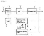
- a conventional example of the receiver will be described with reference to the block diagram of Fig. 1.
- a signal from an input terminal 1 is amplified by a variable gain amplifier 2, passed through an A/D converter 3 and input to a correlator 4.
- An output from correlator 4 is input to a synchronizing circuit, and correlation synchronization is established at the correlated timing.
- the correlated output at that time is compared with an optimally set threshold value by a correlated output comparator 5, the output from comparison is smoothed by a filter 7, and thereafter it is applied to variable gain amplifier 2 so that the gain is controlled.
- the maximum point where correlated output matches hereinafter referred to as correlation spike
- the desired signal level to be input to A/D converter 3 has an optimal value, and it is not the case that any signal level may be input.
- the optimal value is known as the optimal quantization interval and in accordance with this interval, the signal amplitude of the input to A/D converter 3 must be optimized by means of variable gain amplifier 2.
- variable gain amplifier 2 it is difficult to control the amplitude of the signal input to A/D converter 3 to be optimal by variable gain amplifier 2. Therefore, instead, correlation spike is controlled such that it is kept constant.
- the amplitude of the correlation spike is constant.
- the input signal comes to have an optimal amplitude, that is, optimal quantization interval is obtained, and hence the receiver comes to have best performance.
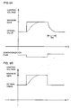
- correlated output comparator 5 correlation spike P shown in Fig. 2A is compared with a threshold value E which is set in advance. Amplitude of correlation spike P varies from time to time. Meanwhile, the threshold value E is the optimal amplitude of the correlation spike. By comparing these two, a difference signal is output. The difference signal is as shown in Fig. 2B. By filtering the difference signal by a filter 7, a waveform shown in Fig. 2C is obtained. The waveform is determined by a constant of filter 7.
- the filter 7 is to average variation caused by noise.
- variable gain amplifier 2 By controlling variable gain amplifier 2 using thus obtained output, the gain of amplifier 2 is lowered when correlated spike P is larger than the threshold value E, and the gain of amplifier 2 is increased when correlation spike P is smaller than the threshold value E. Feedback control is thus realized, whereby the peak of the correlation spike P is kept always matching the set threshold value E.
- correlated output compactor 5 compares the output with the threshold value E regardless of whether it is a correlation spike or not, and using the resulting difference signal, the variable gain amplifier 2 is controlled.
- the initial synchronizing circuit operates to establish synchronization. Thereafter, synchronization is maintained by the synchronization protecting circuit. In this manner, correlation synchronization pulse point is controlled such that it always appears at the correlation spike P.
- the initial synchronizing circuit compares an input signal with a set threshold value (the threshold provided for the synchronizing circuit 6 and not shown in Fig. 1), and if the input signal is higher, it assumes that the input signal is the correlation spike P. By repeating this operation several times at the same timing, synchronization is established.
- variable gain amplifier 2 is subjected to automatic gain control (AGC) so that the output signal from variable gain amplifier 2 is kept constant.
- AGC automatic gain control
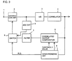
- Fig. 3 shows this structure. Basically, this structure is the same as Fig. 1, except that an AGC circuit 8 is provided at the output of variable gain amplifier 2 for detecting power from the output and for keeping constant the amplitude.
- AGC circuit 8 is equivalent to any AGC circuit used in general communication equipment.
- a switch 9 is switched so that the amplitude of the output from variable gain amplifier 2 is kept constant by the output from AGC circuit 8, and after initial synchronization is established, the variable gain amplifier 2 is controlled referring to the correlated output as shown in Fig. 1. This switching is performed using a synchronization flag FLG output from synchronizing circuit 6, indicating whether or not initial synchronization is established.
- AGC circuit 8 can be implemented by a capacitor or a diode for detection, an analog filter or the like, these elements are all analog devices having large circuit scale and not suitable for integration.
- US 5, 347,534 relates to a spread spectrum receiver including a correlator, variable gain amplifiers and a demodulator, whereon the gain of the amplifiers is controlled in response to a demodulation output from the demodulator.
- An object of the present invention is to provide a spread spectrum signal receiver having a simple structure and capable of stably performing initial synchronization.
- the received signal is amplified by a variable gain amplifier
- an output signal from the amplifier is converted to a digital signal by a converting circuit
- correlation between the value which has been converted to the digital signal and a spread code is found by a correlator, in order to establish correlated synchronization by using correlated output
- a predetermined threshold value and a correlated output are compared by a correlation synchronization circuit so that initial synchronization is established and thereafter synchronization is maintained
- level of an output amplitude of the variable gain amplifier is controlled based on the amplitude of the correlator in response to the establishment of synchronization
- gain of the variable gain amplifier is switched to the maximum gain dependent on presence/absence of a synchronization establishment signal.
- variable gain amplifier is switched to the maximum gain dependent on presence/absence of the synchronization establishment signal, so that the signal amplitude at the time of initial synchronization can be kept at the maximum value.
- a holding circuit is provided for holding the output amplitude value output from the gain control circuit while the synchronization is maintained as a gain control value, and the gain of the variable gain amplifier is controlled by the held gain control value. Therefore, in this embodiment, when the synchronization establishment signal is generated from correlation synchronizing circuit, the control value held from the maximum gain can be set again, and therefore at the time of air link disconnection, a value before disconnection can be readily recovered.
- the gain control value held by the holding circuit is resettable. Therefore, in the preferred embodiment, the value is not always returned to the state before disconnection but it can be changed in accordance with an instruction from an upper layer, such as a protocol.
- a filter for smoothing the output from the gain control circuit is provided, and the time constant of the filter is made variable. Therefore, in the more preferred embodiment, time for convergence to the transitional state period can be made shorter by varying the time constant.
- the performance of the synchronization protecting circuit in the transitional state can be improved.
- FIG. 4 is a circuit block diagram showing the structure of the receiver.
- a signal from input terminal 11 is amplified by variable gain amplifier 12, converted to a digital signal by A/D converter 13 and input to correlator 14.
- An output signal from correlator 14 is input to correlated output comparator 15 as well as to synchronizing circuit 16.
- synchronizing circuit 16 correlated synchronization is established at the correlated timing.
- the correlated output at that time and an optimally set threshold value E are compared by correlated output comparator 15 (compared and a difference signal therebetween is output).
- synchronization flag FLG output separately from synchronizing circuit 16 indicates synchronization. Therefore, switch 19 is switched such that the signal from correlated output comparator 15 is selected, in accordance with the flag FLG.
- the comparison output from the correlated output comparator 15 controls, through switch 19 and filter 17, the gain of variable gain amplifier 12.
- switch 19 passes the output value obtained by comparison to filter 17, so that the maximum point where correlated output matches (hereinafter referred to as the correlation spike) is always kept constant.
- switch 19 selects and outputs the value of maximum gain setting circuit 18 and passes it to filter 17.
- switch 19 and maximum gain setting circuit 18 are necessary. However, these can be implemented in far simpler structure than AGC circuit 8 of Fig. 3.
- A/D converter 13 is used, which may generally have a resolution of 3 or 4 bits. It may have an analog input range of about 1 to about 2V, which voltage range is divided into 8 or 16 levels.
- Figs. 5A and 5B Such operation is shown in Figs. 5A and 5B.
- Fig. 5A corresponds to the optimal amplitude.
- an A/D converter of 3 bits is used, and the input range is divided into 8 levels.
- the magnitude of amplitude the amplitude having such an amplitude corresponding to the eye pattern shown in the figure provides optimal characteristics.
- Fig. 5B corresponds to the maximum amplification of variable gain amplifier 12, in which signal amplitude exceeds 8 levels and all quantized to -7 and 7.
- variable gain amplifier 12 is set to the maximum, whereby initial synchronization can be performed stably with simple structure as compared with the prior art example.
- the maximum gain setting circuit 18 is simply to set the control voltage to the maximum value of variable gain amplifier 12, that is, to a fixed value of 5V, for example. Therefore, as compared with the conventional structure of Fig. 3, the circuit structure is quite simple.
- FIG. 6 A second embodiment of the present invention will be described with reference to Fig. 6.
- Fig. 6 portions corresponding to those of Fig. 4 are denoted by the same reference characters and description thereof is not repeated.
- switch 19 for switching to the maximum gain set value is connected in the succeeding stage of filter 17.
- initial synchronization of correlation is, of course, performed at the start of communication.
- initial synchronization of correlation may be necessary dependent on the condition of communicating wireless transceivers, when the air link is disconnected, for example.
- FIG. 8 A third embodiment of the present invention will be described with reference to Fig. 8.
- portions similar to the second embodiment shown in Fig. 6 are denoted by the same reference characters and description thereof is not repeated.
- holding circuit 20 holds the comparison output from correlated output comparator 15 at that time and when said flag FLG indicates synchronization, applies the held value to filter 17, and in the synchronized state thereafter, passes the output from the correlated output comparator 15 directly to filter 17.
- synchronization flag FLG indicates off-synchronization, and the process for initial synchronization starts.
- the output from filter 17 is again supplied as control signal to variable gain amplifier 12. Difference in operation in that case when holding circuit 20 is provided and not provided will be described with reference to Figs. 9A and 9B.
- Fig. 9A shows an example where holding circuit 20 is not provided.
- the operation is similar to that shown in Fig. 7A, and control voltage is set to the maximum gain.
- convergence to optimal value takes time, because of the integrating characteristic of filter 17. In this case, there is a delay of TD2 until convergence to maximum value is completed.
- the third embodiment in order to hold the voltage of the optimal value at the moment when synchronization is lost is held in the holding circuit 20. Therefore, simultaneously with the reestablishment of synchronization, a level close to the optimal value can be obtained. This is shown in Fig. 9B. As a result, the delay tD2 can be made zero, and performance can be improved.
- FIG. 10 A fourth embodiment of the present invention will be described with reference to Fig. 10.
- the structure is the same as the third embodiment described above (Fig. 8).
- holding circuit 20 is adapted such that an external reset signal RST can be input through terminal 21.
- RST an external reset signal
- the reset signal RST may be generated using the length of the disconnected time as a reference, or generated using end of communication of one packet as a reference, by determining end of a data packet based on the demodulated data.
- the signal is provided from an upper layer (for example, a signal from a protocol).
- a time constant variable filter 17a is used as the filter and variable control thereof is performed by a filter controller 22 which outputs a control signal based on the synchronization flag FLG.
- the time constant of filter 17a is controlled by filter controller 22 in accordance with the time lapse from establishment of synchronization flag.
- the transitional time is determined by the time constant of filter 17a.
- optimal value can be recovered quickly by using holding circuit 20 as in the third embodiment (Fig. 8).
- the transitional time is still determined by the time constant of filter 17a.
- the transitional characteristic is determined by a time constant which is kept constant normally. Therefore, a time tD3 is necessary to attain the steady state. Further, in the present embodiment, the time constant of filter 17a is switched in the time period t3, steady state can be attained in the time period tD4, and hence the speed of operation can be improved.
- the time constant in the initial establishment and in the transitional state, the time constant is set shorter to realize high speed synchronization, while in the steady state, the time constant is set longer to enable stable operation.
- time constant variable filter 17a and filter controller 22 can be applied to any of the first to fourth embodiments to provide similar effects. Further, the time constant of the filter is switched into two steps in time t3 in the above described embodiment. However, it may be switched in several steps or linearly.
- a sixth embodiment of the present invention will be described with reference to Fig. 13.
- the comparison output from correlated output comparator 15 is applied not only to filter 17 but also to the synchronizing circuit 16.
- Synchronizing circuit 16 is divided into initial synchronizing portion 31 and synchronization protecting portion 32 to which an output from correlator 14 is applied respectively through a terminal 30.
- initial synchronization is established in initial synchronizing portion 31, synchronization flag FLG is output, and synchronization protecting process starts.
- a comparator 31a is provided in initial synchronizing portion 31 by which the level of the correlated output and a prescribed threshold value V1 are compared. When the correlated output is larger than the threshold value V1, initial synchronizing operation takes place.
- flag FLG is set to "1" and synchronization protecting portion 32 is informed of the establishment of the initial synchronization.
- synchronization protecting portion 32 maintains synchronization, comparing the correlated output from terminal 30 with a threshold value V2.
- synchronization protecting portion 32 resets itself and also resets the initial synchronizing portion 31.
- the flag FLG is set to "0.”
- Initial synchronizing portion 31 again performs initial synchronization so as to set flag FLG to "1.”
- the threshold value is as shown by the threshold value A of Fig. 15, while for protecting synchronization, the threshold value B for the steady state is used.
- a threshold controller 33 which determines the threshold value in the transitional state using the value of a signal from correlated output comparator 15, and the threshold value is used as the threshold value V2 for the synchronization protecting portion 32.
- the threshold value can be controlled as represented by the solid line a in Fig. 15, and correct synchronization protection becomes possible even in the transitional state.
- the control is performed in the following manner, for example. If the threshold value in the steady state corresponds to 80% of the correlated output, then the threshold value is set by multiplying the output from correlated output comparator 15 plus amplitude in the steady state by 80%.
- fixed threshold V1 is used similar to the above. This embodiment is applicable to any of the first to fifth embodiments.
- means for switching the variable gain amplifier to the maximum gain is provided, and therefore the gain is switched to the maximum value dependent on presence/absence of a synchronization establishment signal from the correlation synchronizing circuit. Accordingly, the signal amplitude at the time of initial synchronization can be kept at the maximum value. Since the gain of the variable amplifier is maximized until initial synchronization is established, initial synchronization can be performed stably with simple structure as compared with the prior art, and the circuit structure can be made simpler as compared with the structure shown in Fig. 3 of the prior art example.
Landscapes
- Engineering & Computer Science (AREA)
- Computer Networks & Wireless Communication (AREA)
- Signal Processing (AREA)
- Synchronisation In Digital Transmission Systems (AREA)
- Control Of Amplification And Gain Control (AREA)
Claims (8)
- Récepteur de signal à étalement de spectre, comprenant :des moyens amplificateurs à gain variable (12) destinés à amplifier un signal reçu ;des moyens de conversion (13) destinés à convertir un signal de sortie provenant desdits moyens amplificateurs à gain variable (12) en un signal numérique ;caractérisé par :des moyens de corrélation (14) destinés à trouver une corrélation entre la valeur convertie par lesdits moyens de conversion (13) en signal numérique et en code propagé ;des moyens de synchronisation de corrélation (16) destinés à comparer un signal de sortie provenant desdits moyens de corrélation (14) avec une valeur seuil prédéterminée afin d'obtenir une corrélation et une synchronisation en utilisant le signal de sortie provenant desdits moyens de corrélation (14) afin de réaliser la synchronisation initiale et une protection de synchronisation après l'établissement de la synchronisation ;des moyens de réglage de la puissance (15) réagissant à l'établissement de la synchronisation par lesdits moyens de synchronisation de corrélation (16) afin de contrôler le niveau d'amplitude de sortie desdits moyens amplificateurs à gain variable (12) sur la base d'une amplitude desdits moyens de corrélation (14) ; etdes moyens de commutation (19) destinés à commuter la puissance desdits moyens amplificateurs à gain variable (12) en une puissance maximale en fonction de la présence ou de l'absence d'un signal d'établissement de synchronisation provenant desdits moyens de synchronisation de corrélation (16).
- Récepteur de signal à étalement de spectre selon la revendication 1, comprenant en outre :des moyens de retenue (20) destinés à retenir une sortie d'amplitude de sortie provenant desdits moyens de réglage de la puissance au moment de la protection de synchronisation en tant que valeur de réglage de la puissance ;dans lequel :la puissance desdits moyens amplificateurs à gain variable est contrôlée par la valeur de réglage de la puissance retenue par lesdits moyens de retenue.
- Récepteur de signal à étalement de spectre selon la revendication 2, comprenant en outre :des moyens (21) destinés à remettre à zéro la valeur de réglage de la puissance retenue par lesdits moyens de retenue.
- Récepteur de signal à étalement de spectre selon la revendication 1, comprenant en outre :des moyens de filtrage (17) destinés à lisser une sortie provenant desdits moyens de commutation et à l'appliquer auxdits moyens amplificateurs à gain variable.
- Récepteur de signal à étalement de spectre selon la revendication 1, comprenant en outre :des moyens de filtrage (17) destinés à lisser une sortie provenant desdits moyens de comparaison et à l'appliquer auxdits moyens de commutation.
- Récepteur de signal à étalement de spectre selon la revendication 5, dans lequel :la constante de temps dudit filtre est rendue variable (17a), ledit récepteur comprenant en outre :des moyens de contrôle de filtrage (22) destinés à modifier ladite constante de temps en fonction d'un intervalle de temps s'écoulant à partir d'un moment d'établissement de ladite synchronisation initiale.
- Récepteur de signal à étalement de spectre selon la revendication 1, dans lequel :lesdits moyens de synchronisation comprennent :des moyens de synchronisation initiale (31) destinés à comparer un signal de sortie provenant desdits moyens de corrélation et une première valeur seuil prédéterminée afin de réaliser une opération de synchronisation initiale lorsque le signal de sortie provenant des moyens de corrélation est supérieur à ladite première valeur seuil prédéterminée, etdes moyens de protection de synchronisation (32) réagissant à l'opération initiale par lesdits moyens de synchronisation initiale afin de comparer un signal de sortie provenant desdits moyens de corrélation avec une seconde valeur seuil prédéterminée, et à protéger la synchronisation après l'établissement de la synchronisation lorsque le signal de sortie provenant desdits moyens de corrélation est supérieur à ladite seconde valeur seuil prédéterminée.
- Récepteur de signal à étalement de spectre selon la revendication 7, comprenant en outre :des moyens de contrôle de la valeur seuil (33) réagissant à un signal de sortie provenant desdits moyens de réglage de la puissance afin de contrôler ladite seconde valeur seuil prédéterminée desdits moyens de protection de synchronisation.
Applications Claiming Priority (3)
| Application Number | Priority Date | Filing Date | Title |
|---|---|---|---|
| JP700996 | 1996-01-19 | ||
| JP700996A JP3273539B2 (ja) | 1996-01-19 | 1996-01-19 | スペクトル拡散信号受信機 |
| JP7009/96 | 1996-01-19 |
Publications (3)
| Publication Number | Publication Date |
|---|---|
| EP0785632A2 EP0785632A2 (fr) | 1997-07-23 |
| EP0785632A3 EP0785632A3 (fr) | 2000-10-18 |
| EP0785632B1 true EP0785632B1 (fr) | 2006-05-10 |
Family
ID=11654065
Family Applications (1)
| Application Number | Title | Priority Date | Filing Date |
|---|---|---|---|
| EP19970300284 Expired - Lifetime EP0785632B1 (fr) | 1996-01-19 | 1997-01-17 | Récepteur à spectre dispersé |
Country Status (4)
| Country | Link |
|---|---|
| US (1) | US5896423A (fr) |
| EP (1) | EP0785632B1 (fr) |
| JP (1) | JP3273539B2 (fr) |
| DE (1) | DE69735831T2 (fr) |
Families Citing this family (21)
| Publication number | Priority date | Publication date | Assignee | Title |
|---|---|---|---|---|
| JPH09261128A (ja) * | 1996-03-22 | 1997-10-03 | Matsushita Electric Ind Co Ltd | スペクトル拡散通信機 |
| JP2751959B2 (ja) * | 1996-07-15 | 1998-05-18 | 日本電気株式会社 | Cdma受信装置の受信タイミング検出回路 |
| JP3408944B2 (ja) * | 1997-04-24 | 2003-05-19 | シャープ株式会社 | スペクトル直接拡散通信システムにおける復調装置及び同システムにおける相関器 |
| US6324229B1 (en) * | 1998-05-11 | 2001-11-27 | Motorola, Inc. | Self-clocking automatic digital level control method and apparatus |
| US6173351B1 (en) * | 1998-06-15 | 2001-01-09 | Sun Microsystems, Inc. | Multi-processor system bridge |
| KR100378058B1 (ko) * | 1998-09-28 | 2003-03-29 | 마쯔시다덴기산교 가부시키가이샤 | Vsb수신기 |
| JP2000269759A (ja) * | 1999-03-18 | 2000-09-29 | Matsushita Electric Ind Co Ltd | 自動利得制御回路およびその回路を備えた受信装置、受信装置における自動利得制御方法、並びに、記録媒体 |
| JP3519338B2 (ja) | 2000-03-24 | 2004-04-12 | 松下電器産業株式会社 | 受信装置及び利得制御方法 |
| US7076225B2 (en) | 2001-02-16 | 2006-07-11 | Qualcomm Incorporated | Variable gain selection in direct conversion receiver |
| US6584355B2 (en) * | 2001-04-10 | 2003-06-24 | Cardiac Pacemakers, Inc. | System and method for measuring battery current |
| CN1314219C (zh) * | 2001-06-18 | 2007-05-02 | 皇家菲利浦电子有限公司 | 峰值检测精度 |
| EP1315292B1 (fr) * | 2001-11-21 | 2006-09-13 | Sony Deutschland GmbH | Commande automatique de gain numérique |
| US7394877B2 (en) * | 2001-12-20 | 2008-07-01 | Texas Instruments Incorporated | Low-power packet detection using decimated correlation |
| US7660344B2 (en) * | 2002-06-28 | 2010-02-09 | Bwa Technology, Inc. | AGC fine-tuning by the adaptive time domain equalizer |
| US7239146B2 (en) * | 2003-07-11 | 2007-07-03 | Cardiac Pacemakers, Inc. | Indicator of remaining energy in storage cell of implantable medical device |
| US6940255B2 (en) * | 2003-10-23 | 2005-09-06 | Cardiac Pacemakers, Inc. | Battery charge indicator such as for an implantable medical device |
| US7194308B2 (en) | 2003-11-12 | 2007-03-20 | Cardiac Pacemakers, Inc. | System and method for monitoring or reporting battery status of implantable medical device |
| JP2005202549A (ja) * | 2004-01-14 | 2005-07-28 | Nec Corp | リセット回路およびリセット方法 |
| WO2012176139A1 (fr) * | 2011-06-22 | 2012-12-27 | Renesas Mobile Corporation | Procédé, appareil et programme d'ordinateur pour le réglage d'un gain de radiofréquence |
| US10484028B2 (en) | 2015-04-15 | 2019-11-19 | Commscope Technologies Llc | Squelch sub-system using correlation between uplink paths |
| JP7004503B2 (ja) * | 2017-01-27 | 2022-01-21 | ラピスセミコンダクタ株式会社 | 自動利得制御回路(agc)、逆拡散回路及び受信データの再生方法 |
Family Cites Families (7)
| Publication number | Priority date | Publication date | Assignee | Title |
|---|---|---|---|---|
| JPS60145713A (ja) * | 1984-01-10 | 1985-08-01 | Fujitsu Ltd | 自動利得制御方式 |
| US5347534A (en) * | 1987-07-31 | 1994-09-13 | Clarion Co., Ltd. | Automatic gain control system |
| US5347537A (en) * | 1992-03-17 | 1994-09-13 | Clarion Co., Ltd. | Spread spectrum communication device |
| WO1995005038A1 (fr) * | 1993-08-11 | 1995-02-16 | Ntt Mobile Communications Network Inc. | Appareil de commande automatique de gain, appareil de communications et procede de commande automatique de gain |
| JP3183078B2 (ja) * | 1994-02-28 | 2001-07-03 | 三菱電機株式会社 | 制御信号生成回路、これを用いた自動利得制御回路、これを用いた受信機及びこれを用いた通信システム |
| JPH08335901A (ja) * | 1995-06-09 | 1996-12-17 | Fujitsu General Ltd | ダイバーシチ回路 |
| JP3113549U (ja) | 2004-12-01 | 2005-09-08 | 直美 四元 | Love缶 |
-
1996
- 1996-01-19 JP JP700996A patent/JP3273539B2/ja not_active Expired - Fee Related
-
1997
- 1997-01-15 US US08/782,668 patent/US5896423A/en not_active Expired - Fee Related
- 1997-01-17 DE DE1997635831 patent/DE69735831T2/de not_active Expired - Fee Related
- 1997-01-17 EP EP19970300284 patent/EP0785632B1/fr not_active Expired - Lifetime
Also Published As
| Publication number | Publication date |
|---|---|
| JPH09200080A (ja) | 1997-07-31 |
| EP0785632A3 (fr) | 2000-10-18 |
| DE69735831T2 (de) | 2007-05-31 |
| US5896423A (en) | 1999-04-20 |
| EP0785632A2 (fr) | 1997-07-23 |
| JP3273539B2 (ja) | 2002-04-08 |
| DE69735831D1 (de) | 2006-06-14 |
Similar Documents
| Publication | Publication Date | Title |
|---|---|---|
| US5896423A (en) | Spread spectrum signal receiver | |
| KR100615022B1 (ko) | 무선수신기 및 무선신호 처리방법 | |
| CA2063364C (fr) | Recepteur de radiotelephonie a generation amelioree d'indications d'intensite de signal recu | |
| JP3493424B2 (ja) | Cdma方式の送信電力制御方法 | |
| GB2285355A (en) | Gain control of amplifier for TDMA signals | |
| US7149263B2 (en) | AGC method and circuit for digital radio receiver | |
| EP0630106A1 (fr) | Dispositif de commande de gain automatique | |
| JPS6165551A (ja) | タイミング位相制御装置 | |
| US7116942B2 (en) | Radio communication apparatus and method of controlling the same | |
| KR100940799B1 (ko) | 버스트로 송신되는 신호의 수신기용 이득 제어 방법, 및 이 방법을 이용하는 수신기 | |
| JP2003125012A (ja) | Agc付きask復調装置 | |
| US20020052187A1 (en) | Receiver used in spread spectrum communication system | |
| JPS6137813B2 (fr) | ||
| KR0168969B1 (ko) | 무선 주파수 신호의 자동 이득 제어 조정 장치 | |
| JP2827581B2 (ja) | ディジタル受信機 | |
| KR100241764B1 (ko) | 고화질 텔레비젼용 자동이득 제어장치 | |
| JPH05122153A (ja) | 光受信回路 | |
| JP4292655B2 (ja) | サンプリング装置 | |
| JP2003124909A (ja) | 自動利得制御装置および自動利得制御方法 | |
| JPH10322150A (ja) | スペクトラム拡散通信の受信装置および自動利得制御方法 | |
| JPH0669128B2 (ja) | 自動利得制御増幅器 | |
| JPH08335901A (ja) | ダイバーシチ回路 | |
| JPH07307723A (ja) | アンテナダイバーシティ制御装置 | |
| JPH09321560A (ja) | スペクトル拡散通信における利得制御回路 | |
| JP3504080B2 (ja) | バースト信号受信装置 |
Legal Events
| Date | Code | Title | Description |
|---|---|---|---|
| PUAI | Public reference made under article 153(3) epc to a published international application that has entered the european phase |
Free format text: ORIGINAL CODE: 0009012 |
|
| AK | Designated contracting states |
Kind code of ref document: A2 Designated state(s): DE FR GB |
|
| PUAL | Search report despatched |
Free format text: ORIGINAL CODE: 0009013 |
|
| AK | Designated contracting states |
Kind code of ref document: A3 Designated state(s): DE FR GB |
|
| RIC1 | Information provided on ipc code assigned before grant |
Free format text: 7H 04B 7/005 A, 7H 03G 3/30 B, 7H 04B 1/16 B |
|
| 17P | Request for examination filed |
Effective date: 20010309 |
|
| 17Q | First examination report despatched |
Effective date: 20050324 |
|
| GRAP | Despatch of communication of intention to grant a patent |
Free format text: ORIGINAL CODE: EPIDOSNIGR1 |
|
| GRAS | Grant fee paid |
Free format text: ORIGINAL CODE: EPIDOSNIGR3 |
|
| GRAA | (expected) grant |
Free format text: ORIGINAL CODE: 0009210 |
|
| AK | Designated contracting states |
Kind code of ref document: B1 Designated state(s): DE FR GB |
|
| REG | Reference to a national code |
Ref country code: GB Ref legal event code: FG4D |
|
| REF | Corresponds to: |
Ref document number: 69735831 Country of ref document: DE Date of ref document: 20060614 Kind code of ref document: P |
|
| ET | Fr: translation filed | ||
| PGFP | Annual fee paid to national office [announced via postgrant information from national office to epo] |
Ref country code: DE Payment date: 20070111 Year of fee payment: 11 |
|
| PGFP | Annual fee paid to national office [announced via postgrant information from national office to epo] |
Ref country code: GB Payment date: 20070117 Year of fee payment: 11 |
|
| PLBE | No opposition filed within time limit |
Free format text: ORIGINAL CODE: 0009261 |
|
| STAA | Information on the status of an ep patent application or granted ep patent |
Free format text: STATUS: NO OPPOSITION FILED WITHIN TIME LIMIT |
|
| 26N | No opposition filed |
Effective date: 20070213 |
|
| PGFP | Annual fee paid to national office [announced via postgrant information from national office to epo] |
Ref country code: FR Payment date: 20070109 Year of fee payment: 11 |
|
| GBPC | Gb: european patent ceased through non-payment of renewal fee |
Effective date: 20080117 |
|
| PG25 | Lapsed in a contracting state [announced via postgrant information from national office to epo] |
Ref country code: DE Free format text: LAPSE BECAUSE OF NON-PAYMENT OF DUE FEES Effective date: 20080801 |
|
| REG | Reference to a national code |
Ref country code: FR Ref legal event code: ST Effective date: 20081029 |
|
| PG25 | Lapsed in a contracting state [announced via postgrant information from national office to epo] |
Ref country code: GB Free format text: LAPSE BECAUSE OF NON-PAYMENT OF DUE FEES Effective date: 20080117 |
|
| PG25 | Lapsed in a contracting state [announced via postgrant information from national office to epo] |
Ref country code: FR Free format text: LAPSE BECAUSE OF NON-PAYMENT OF DUE FEES Effective date: 20080131 |