EP0786808B1 - Gedruckte Schaltungsplatte oder Halbleitervorrichtung mit anisotrop leitenden Platten - Google Patents
Gedruckte Schaltungsplatte oder Halbleitervorrichtung mit anisotrop leitenden Platten Download PDFInfo
- Publication number
- EP0786808B1 EP0786808B1 EP97300275A EP97300275A EP0786808B1 EP 0786808 B1 EP0786808 B1 EP 0786808B1 EP 97300275 A EP97300275 A EP 97300275A EP 97300275 A EP97300275 A EP 97300275A EP 0786808 B1 EP0786808 B1 EP 0786808B1
- Authority
- EP
- European Patent Office
- Prior art keywords
- anisotropic conductive
- conductive sheet
- sheets
- circuit pattern
- sheet
- Prior art date
- Legal status (The legal status is an assumption and is not a legal conclusion. Google has not performed a legal analysis and makes no representation as to the accuracy of the status listed.)
- Expired - Lifetime
Links
Images


Classifications
-
- H—ELECTRICITY
- H10—SEMICONDUCTOR DEVICES; ELECTRIC SOLID-STATE DEVICES NOT OTHERWISE PROVIDED FOR
- H10W—GENERIC PACKAGES, INTERCONNECTIONS, CONNECTORS OR OTHER CONSTRUCTIONAL DETAILS OF DEVICES COVERED BY CLASS H10
- H10W72/00—Interconnections or connectors in packages
- H10W72/30—Die-attach connectors
-
- H—ELECTRICITY
- H05—ELECTRIC TECHNIQUES NOT OTHERWISE PROVIDED FOR
- H05K—PRINTED CIRCUITS; CASINGS OR CONSTRUCTIONAL DETAILS OF ELECTRIC APPARATUS; MANUFACTURE OF ASSEMBLAGES OF ELECTRICAL COMPONENTS
- H05K3/00—Apparatus or processes for manufacturing printed circuits
- H05K3/46—Manufacturing multilayer circuits
- H05K3/4611—Manufacturing multilayer circuits by laminating two or more circuit boards
- H05K3/4614—Manufacturing multilayer circuits by laminating two or more circuit boards the electrical connections between the circuit boards being made during lamination
- H05K3/4617—Manufacturing multilayer circuits by laminating two or more circuit boards the electrical connections between the circuit boards being made during lamination characterized by laminating only or mainly similar single-sided circuit boards
-
- H—ELECTRICITY
- H10—SEMICONDUCTOR DEVICES; ELECTRIC SOLID-STATE DEVICES NOT OTHERWISE PROVIDED FOR
- H10W—GENERIC PACKAGES, INTERCONNECTIONS, CONNECTORS OR OTHER CONSTRUCTIONAL DETAILS OF DEVICES COVERED BY CLASS H10
- H10W20/00—Interconnections in chips, wafers or substrates
- H10W20/40—Interconnections external to wafers or substrates, e.g. back-end-of-line [BEOL] metallisations or vias connecting to gate electrodes
- H10W20/41—Interconnections external to wafers or substrates, e.g. back-end-of-line [BEOL] metallisations or vias connecting to gate electrodes characterised by their conductive parts
- H10W20/44—Conductive materials thereof
- H10W20/4473—Conductive organic materials, e.g. conductive adhesives or conductive inks
-
- H—ELECTRICITY
- H10—SEMICONDUCTOR DEVICES; ELECTRIC SOLID-STATE DEVICES NOT OTHERWISE PROVIDED FOR
- H10W—GENERIC PACKAGES, INTERCONNECTIONS, CONNECTORS OR OTHER CONSTRUCTIONAL DETAILS OF DEVICES COVERED BY CLASS H10
- H10W70/00—Package substrates; Interposers; Redistribution layers [RDL]
- H10W70/60—Insulating or insulated package substrates; Interposers; Redistribution layers
- H10W70/62—Insulating or insulated package substrates; Interposers; Redistribution layers characterised by their interconnections
- H10W70/63—Vias, e.g. via plugs
- H10W70/635—Through-vias
-
- H—ELECTRICITY
- H10—SEMICONDUCTOR DEVICES; ELECTRIC SOLID-STATE DEVICES NOT OTHERWISE PROVIDED FOR
- H10W—GENERIC PACKAGES, INTERCONNECTIONS, CONNECTORS OR OTHER CONSTRUCTIONAL DETAILS OF DEVICES COVERED BY CLASS H10
- H10W90/00—Package configurations
- H10W90/701—Package configurations characterised by the relative positions of pads or connectors relative to package parts
-
- H—ELECTRICITY
- H05—ELECTRIC TECHNIQUES NOT OTHERWISE PROVIDED FOR
- H05K—PRINTED CIRCUITS; CASINGS OR CONSTRUCTIONAL DETAILS OF ELECTRIC APPARATUS; MANUFACTURE OF ASSEMBLAGES OF ELECTRICAL COMPONENTS
- H05K1/00—Printed circuits
- H05K1/02—Details
- H05K1/03—Use of materials for the substrate
- H05K1/0313—Organic insulating material
- H05K1/0353—Organic insulating material consisting of two or more materials, e.g. two or more polymers, polymer + filler, + reinforcement
- H05K1/0373—Organic insulating material consisting of two or more materials, e.g. two or more polymers, polymer + filler, + reinforcement containing additives, e.g. fillers
-
- H—ELECTRICITY
- H05—ELECTRIC TECHNIQUES NOT OTHERWISE PROVIDED FOR
- H05K—PRINTED CIRCUITS; CASINGS OR CONSTRUCTIONAL DETAILS OF ELECTRIC APPARATUS; MANUFACTURE OF ASSEMBLAGES OF ELECTRICAL COMPONENTS
- H05K2201/00—Indexing scheme relating to printed circuits covered by H05K1/00
- H05K2201/02—Fillers; Particles; Fibers; Reinforcement materials
- H05K2201/0203—Fillers and particles
- H05K2201/0206—Materials
- H05K2201/0215—Metallic fillers
-
- H—ELECTRICITY
- H05—ELECTRIC TECHNIQUES NOT OTHERWISE PROVIDED FOR
- H05K—PRINTED CIRCUITS; CASINGS OR CONSTRUCTIONAL DETAILS OF ELECTRIC APPARATUS; MANUFACTURE OF ASSEMBLAGES OF ELECTRICAL COMPONENTS
- H05K3/00—Apparatus or processes for manufacturing printed circuits
- H05K3/30—Assembling printed circuits with electric components, e.g. with resistors
- H05K3/32—Assembling printed circuits with electric components, e.g. with resistors electrically connecting electric components or wires to printed circuits
- H05K3/321—Assembling printed circuits with electric components, e.g. with resistors electrically connecting electric components or wires to printed circuits by conductive adhesives
- H05K3/323—Assembling printed circuits with electric components, e.g. with resistors electrically connecting electric components or wires to printed circuits by conductive adhesives by applying an anisotropic conductive adhesive layer over an array of pads
-
- H—ELECTRICITY
- H05—ELECTRIC TECHNIQUES NOT OTHERWISE PROVIDED FOR
- H05K—PRINTED CIRCUITS; CASINGS OR CONSTRUCTIONAL DETAILS OF ELECTRIC APPARATUS; MANUFACTURE OF ASSEMBLAGES OF ELECTRICAL COMPONENTS
- H05K3/00—Apparatus or processes for manufacturing printed circuits
- H05K3/40—Forming printed elements for providing electric connections to or between printed circuits
- H05K3/4038—Through-connections; Vertical interconnect access [VIA] connections
- H05K3/4084—Through-connections; Vertical interconnect access [VIA] connections by deforming at least one of the conductive layers
-
- H—ELECTRICITY
- H05—ELECTRIC TECHNIQUES NOT OTHERWISE PROVIDED FOR
- H05K—PRINTED CIRCUITS; CASINGS OR CONSTRUCTIONAL DETAILS OF ELECTRIC APPARATUS; MANUFACTURE OF ASSEMBLAGES OF ELECTRICAL COMPONENTS
- H05K3/00—Apparatus or processes for manufacturing printed circuits
- H05K3/46—Manufacturing multilayer circuits
- H05K3/4644—Manufacturing multilayer circuits by building the multilayer layer by layer, i.e. build-up multilayer circuits
- H05K3/4647—Manufacturing multilayer circuits by building the multilayer layer by layer, i.e. build-up multilayer circuits by applying an insulating layer around previously made via studs
-
- H—ELECTRICITY
- H10—SEMICONDUCTOR DEVICES; ELECTRIC SOLID-STATE DEVICES NOT OTHERWISE PROVIDED FOR
- H10W—GENERIC PACKAGES, INTERCONNECTIONS, CONNECTORS OR OTHER CONSTRUCTIONAL DETAILS OF DEVICES COVERED BY CLASS H10
- H10W70/00—Package substrates; Interposers; Redistribution layers [RDL]
- H10W70/60—Insulating or insulated package substrates; Interposers; Redistribution layers
- H10W70/62—Insulating or insulated package substrates; Interposers; Redistribution layers characterised by their interconnections
- H10W70/65—Shapes or dispositions of interconnections
- H10W70/654—Top-view layouts
- H10W70/656—Fan-in layouts
-
- H—ELECTRICITY
- H10—SEMICONDUCTOR DEVICES; ELECTRIC SOLID-STATE DEVICES NOT OTHERWISE PROVIDED FOR
- H10W—GENERIC PACKAGES, INTERCONNECTIONS, CONNECTORS OR OTHER CONSTRUCTIONAL DETAILS OF DEVICES COVERED BY CLASS H10
- H10W70/00—Package substrates; Interposers; Redistribution layers [RDL]
- H10W70/60—Insulating or insulated package substrates; Interposers; Redistribution layers
- H10W70/67—Insulating or insulated package substrates; Interposers; Redistribution layers characterised by their insulating layers or insulating parts
- H10W70/68—Shapes or dispositions thereof
- H10W70/685—Shapes or dispositions thereof comprising multiple insulating layers
-
- H—ELECTRICITY
- H10—SEMICONDUCTOR DEVICES; ELECTRIC SOLID-STATE DEVICES NOT OTHERWISE PROVIDED FOR
- H10W—GENERIC PACKAGES, INTERCONNECTIONS, CONNECTORS OR OTHER CONSTRUCTIONAL DETAILS OF DEVICES COVERED BY CLASS H10
- H10W72/00—Interconnections or connectors in packages
- H10W72/071—Connecting or disconnecting
- H10W72/073—Connecting or disconnecting of die-attach connectors
- H10W72/07331—Connecting techniques
-
- H—ELECTRICITY
- H10—SEMICONDUCTOR DEVICES; ELECTRIC SOLID-STATE DEVICES NOT OTHERWISE PROVIDED FOR
- H10W—GENERIC PACKAGES, INTERCONNECTIONS, CONNECTORS OR OTHER CONSTRUCTIONAL DETAILS OF DEVICES COVERED BY CLASS H10
- H10W72/00—Interconnections or connectors in packages
- H10W72/071—Connecting or disconnecting
- H10W72/074—Connecting or disconnecting of anisotropic conductive adhesives
-
- H—ELECTRICITY
- H10—SEMICONDUCTOR DEVICES; ELECTRIC SOLID-STATE DEVICES NOT OTHERWISE PROVIDED FOR
- H10W—GENERIC PACKAGES, INTERCONNECTIONS, CONNECTORS OR OTHER CONSTRUCTIONAL DETAILS OF DEVICES COVERED BY CLASS H10
- H10W72/00—Interconnections or connectors in packages
- H10W72/20—Bump connectors, e.g. solder bumps or copper pillars; Dummy bumps; Thermal bumps
- H10W72/231—Shapes
- H10W72/234—Cross-sectional shape, i.e. in side view
-
- H—ELECTRICITY
- H10—SEMICONDUCTOR DEVICES; ELECTRIC SOLID-STATE DEVICES NOT OTHERWISE PROVIDED FOR
- H10W—GENERIC PACKAGES, INTERCONNECTIONS, CONNECTORS OR OTHER CONSTRUCTIONAL DETAILS OF DEVICES COVERED BY CLASS H10
- H10W72/00—Interconnections or connectors in packages
- H10W72/20—Bump connectors, e.g. solder bumps or copper pillars; Dummy bumps; Thermal bumps
- H10W72/241—Dispositions, e.g. layouts
- H10W72/242—Dispositions, e.g. layouts relative to the surface, e.g. recessed, protruding
-
- H—ELECTRICITY
- H10—SEMICONDUCTOR DEVICES; ELECTRIC SOLID-STATE DEVICES NOT OTHERWISE PROVIDED FOR
- H10W—GENERIC PACKAGES, INTERCONNECTIONS, CONNECTORS OR OTHER CONSTRUCTIONAL DETAILS OF DEVICES COVERED BY CLASS H10
- H10W72/00—Interconnections or connectors in packages
- H10W72/20—Bump connectors, e.g. solder bumps or copper pillars; Dummy bumps; Thermal bumps
- H10W72/251—Materials
- H10W72/252—Materials comprising solid metals or solid metalloids, e.g. PbSn, Ag or Cu
-
- H—ELECTRICITY
- H10—SEMICONDUCTOR DEVICES; ELECTRIC SOLID-STATE DEVICES NOT OTHERWISE PROVIDED FOR
- H10W—GENERIC PACKAGES, INTERCONNECTIONS, CONNECTORS OR OTHER CONSTRUCTIONAL DETAILS OF DEVICES COVERED BY CLASS H10
- H10W72/00—Interconnections or connectors in packages
- H10W72/20—Bump connectors, e.g. solder bumps or copper pillars; Dummy bumps; Thermal bumps
- H10W72/261—Functions other than electrical connecting
-
- H—ELECTRICITY
- H10—SEMICONDUCTOR DEVICES; ELECTRIC SOLID-STATE DEVICES NOT OTHERWISE PROVIDED FOR
- H10W—GENERIC PACKAGES, INTERCONNECTIONS, CONNECTORS OR OTHER CONSTRUCTIONAL DETAILS OF DEVICES COVERED BY CLASS H10
- H10W72/00—Interconnections or connectors in packages
- H10W72/30—Die-attach connectors
- H10W72/321—Structures or relative sizes of die-attach connectors
- H10W72/325—Die-attach connectors having a filler embedded in a matrix
-
- H—ELECTRICITY
- H10—SEMICONDUCTOR DEVICES; ELECTRIC SOLID-STATE DEVICES NOT OTHERWISE PROVIDED FOR
- H10W—GENERIC PACKAGES, INTERCONNECTIONS, CONNECTORS OR OTHER CONSTRUCTIONAL DETAILS OF DEVICES COVERED BY CLASS H10
- H10W72/00—Interconnections or connectors in packages
- H10W72/30—Die-attach connectors
- H10W72/351—Materials of die-attach connectors
- H10W72/352—Materials of die-attach connectors comprising metals or metalloids, e.g. solders
-
- H—ELECTRICITY
- H10—SEMICONDUCTOR DEVICES; ELECTRIC SOLID-STATE DEVICES NOT OTHERWISE PROVIDED FOR
- H10W—GENERIC PACKAGES, INTERCONNECTIONS, CONNECTORS OR OTHER CONSTRUCTIONAL DETAILS OF DEVICES COVERED BY CLASS H10
- H10W72/00—Interconnections or connectors in packages
- H10W72/30—Die-attach connectors
- H10W72/351—Materials of die-attach connectors
- H10W72/353—Materials of die-attach connectors not comprising solid metals or solid metalloids, e.g. ceramics
- H10W72/354—Materials of die-attach connectors not comprising solid metals or solid metalloids, e.g. ceramics comprising polymers
-
- H—ELECTRICITY
- H10—SEMICONDUCTOR DEVICES; ELECTRIC SOLID-STATE DEVICES NOT OTHERWISE PROVIDED FOR
- H10W—GENERIC PACKAGES, INTERCONNECTIONS, CONNECTORS OR OTHER CONSTRUCTIONAL DETAILS OF DEVICES COVERED BY CLASS H10
- H10W72/00—Interconnections or connectors in packages
- H10W72/90—Bond pads, in general
- H10W72/921—Structures or relative sizes of bond pads
- H10W72/923—Bond pads having multiple stacked layers
-
- H—ELECTRICITY
- H10—SEMICONDUCTOR DEVICES; ELECTRIC SOLID-STATE DEVICES NOT OTHERWISE PROVIDED FOR
- H10W—GENERIC PACKAGES, INTERCONNECTIONS, CONNECTORS OR OTHER CONSTRUCTIONAL DETAILS OF DEVICES COVERED BY CLASS H10
- H10W72/00—Interconnections or connectors in packages
- H10W72/90—Bond pads, in general
- H10W72/941—Dispositions of bond pads
- H10W72/944—Dispositions of multiple bond pads
- H10W72/9445—Top-view layouts, e.g. mirror arrays
-
- H—ELECTRICITY
- H10—SEMICONDUCTOR DEVICES; ELECTRIC SOLID-STATE DEVICES NOT OTHERWISE PROVIDED FOR
- H10W—GENERIC PACKAGES, INTERCONNECTIONS, CONNECTORS OR OTHER CONSTRUCTIONAL DETAILS OF DEVICES COVERED BY CLASS H10
- H10W72/00—Interconnections or connectors in packages
- H10W72/90—Bond pads, in general
- H10W72/951—Materials of bond pads
- H10W72/952—Materials of bond pads comprising metals or metalloids, e.g. PbSn, Ag or Cu
Definitions
- the present invention relates to an anisotropic conductive sheet with a conductive layer and a printed circuit board using the same.
- the present invention also relates to a semiconductor device using such an anisotropic conductive sheet.
- a multilayer type printed circuit board consisting of a plurality of resin substrates, each carrying circuit patterns on its surface, has been known in the art.
- JP-A-4017346 discloses an anisotropic conductive film which is used to connect an electrode of a semiconductor chip to a lead by laying a conductive pattern on the anisotropic conductive sheet and pressing the anisotropic conductive film at certain points to make it conductive.
- US-A-5010038 discloses a method of increasing the number of contacts available on a semiconductor chip by forming contacts on the base of the chip and mounting the chip on an elastic pad with conductive vias formed in it. The elastic pad simultaneously urges the chip into contact with a heat sink cover and provides electrical connection to a substrate.
- EP-A-0734065 discloses a chip sized semiconductor device which uses an anisotropic conductive sheet to connect a chip with a circuit pattern.
- An object of the present invention is to provide a multilayer type circuit board having a smaller thickness, which can be easily produced because the electric-connections between upper and lower circuit patterns are simple, and an anisotropic conductive sheet with a conductive layer suitably used for producing such a circuit board.
- a circuit board comprising:
- Bumps may be provided on the circuit pattern formed on the substrate and the anisotropic conductive sheets, except for the uppermost anisotropic conductive sheet.
- the anisotropic conductive sheets are laminated on said bumps and partially pressed by the bumps so that the pressed portions of the anisotropic conductive sheets are electrically conductive and thus said circuit pattern on said substrate and said circuit pattern on said anisotropic conductive sheets are electrically connected to each other.
- At least one of the circuit patterns formed on the substrate and on the plurality of anisotropic conductive sheets may be a power supply conductive layer formed over the entire surface.
- At least one of the circuit patterns formed on the substrate and on the plurality of anisotropic conductive sheets may be a ground conductive layer formed over the entire surface.
- a semiconductor device comprising: a semiconductor chip having upper and lower surfaces, the chip having electrodes formed on the upper surface; an electrically insulating passivation film formed on the upper surface of the semiconductor chip, except for areas where the electrodes exist; a plurality of anisotropic conductive sheets consisting of a basic material of resin and conductive metal particles dispersed in the basic material, each having upper and lower surfaces, a circuit pattern being formed on the upper surface of the respective anisotropic conductive sheet; the plurality of anisotropic conductive sheets being laminated on each other in such a manner that the lower surface of each.
- anisotropic conductive sheet is adhered to the upper surface of the adjacent anisotropic conductive sheet; the upper surface of the semiconductor chip is adhered to the lower surface of the lowermost anisotropic conductive sheet; the circuit patterns on the plurality of anisotropic conductive sheets; and the electrodes of the semiconductor chip being electrically connected to each other by means of the plurality of anisotropic sheets; an electrically insulative layer formed on the upper surface of the uppermost anisotropic conductive sheet to cover the circuit pattern thereof, except for external connecting portions thereof which are exposed; and external connecting terminals formed on the respective external connecting portions.
- the lowermost anisotropic conductive sheet can be mechanically pressed partially beforehand at positions corresponding to the electrodes by means of a press bonding tool, so that the pressed portions of the lowermost anisotropic conductive sheet are electrically conductive and thus said electrodes of the semiconductor chip and said circuit pattern on said lowermost anisotropic conductive sheet are electrically connected to each other.
- the electrodes of the semiconductor chip can be provided with conductive bumps which protrude upward over the passivation film, so that the lowermost anisotropic conductive sheet is laminated on said bumps partially pressed by the bumps and, therefore, the pressed portions of the lowermost anisotropic conductive sheet are electrically conductive and thus said electrodes of the semiconductor chip and said circuit pattern on said lowermost anisotropic conductive sheet are electrically connected to each other.
- the external connecting terminals may be solder bumps.
- FIG. 1 is a side sectional view of a semiconductor device 30 using an anisotropic conductive sheet with a conductive layer described later.
- Reference numerals 32 denotes a semiconductor chip; 34, a passivation film made of SiO 2 or others; and 36, an Al pad (pad section) built in the semiconductor chip 32.
- the passivation film 34 is not formed in an area where the Al pad 36 exists, so that the Al pad 36 is exposed.
- a number of Al pads 36 are formed in a desired pattern on the semiconductor chip 32.
- Reference numeral 38 denotes an anisotropic conductive sheet formed while covering the passivation film 34.
- the anisotropic conductive sheet 38 is formed of a resin containing a conductive filler 39 (Fig. 2) such as a metallic powder, and, by the application of pressure, becomes conductive in the pressed direction due to the continuity of the conductive filler 39.
- Reference numeral 40 denotes a circuit pattern formed on the anisotropic conductive sheet 38 in a predetermined pattern.
- the circuit pattern 40 is formed so that it presses the anisotropic conductive sheet 38 as shown in Fig. 2, whereby that portion of the anisotropic conductive sheet 38 is conductive to electrically connect the Al pad 36 with the circuit pattern 40.
- the circuit pattern 40 is formed by adhering a metallic foil such as a copper foil to the anisotropic conductive sheet 38 and then etching the same to leave a desired pattern.
- a metallic layer such as a copper layer or an aluminum layer may be formed by a sputtering method, which is then etched to obtain a desired pattern.
- Reference numeral 42 is a photosensitive resist film (insulation film) covering the anisotropic conductive sheet 38 and the circuit pattern 40.
- the photosensitive resist film 42 is a protective film for the circuit pattern 40 and may be formed of various types of photosensitive solder resist.
- Through-holes 44 are formed at suitable locations in the photosensitive resist film 42 corresponding to the respective circuit patterns 40, for example, in a matrix arrangement (so that a contact 40a in the circuit patterns 40 to which an external terminal is to be connected is exposed from the respective via-hole 44).
- Reference numeral 46 denotes a bump forming an external terminal which is arranged to be electrically connected with the respective contact 40a via the respective via-hole 44 and projects above the photosensitive resist film 42.
- the bump 46 may be formed as a ball bump such as a solder ball as shown in the drawing, but may be formed as a flat land or others. Or a lead pin may be connected as an external terminal.
- the bump may be formed by a plating such as a nickel/gold plating.
- Reference numeral 48 denotes a protective film formed while covering a side wall of the semiconductor chip 32, the passivation film 34 and the anisotropic conductive sheet 38 to prevent the moisture from invading through the boundaries between the respective layers.
- the protective film 48 may be formed by using a suitable resinous resist, but is not indispensable. Also, instead of the protective film 48, a frame made of a metal or the like may be bonded.
- the semiconductor device 30 is constructed as described above, it is possible to have a size equal to that of the semiconductor chip 32.
- the semiconductor device 30 becomes thinner.
- anisotropic conductive sheet 38 and of the photosensitive resist film 42 can function as a shock absorbing layer for protecting a surface of the semiconductor chip 32.
- a back surface of the semiconductor chip 32 is preferably exposed to enhance the heat radiation.
- a heat sink or a heat spreader may be bonded thereto.
- Fig. 3 illustrates another example of a semiconductor device useful for illustrating the present invention.
- a bump 37 made, for example, of Au is provided on an Al pad 36 of a semiconductor chip 32 to be higher than a passivation film 34, so that a portion of an anisotropic conductive sheet 38 is pressed by the projected bump 37 when the anisotropic conductive sheet 38 is bonded onto the passivation film 34 to cause that portion of the anisotropic conductive sheet 38 to be conductive and thus electrically connect the Al pad 36 to the circuit pattern 40.
- this example is advantageous in that the circuit pattern 40 can be generally flat to facilitate lamination.
- Figs. 4 and 5 illustrate a process for producing the semiconductor device shown in Fig. 1.
- a metallic foil such as a copper foil is bonded to an anisotropic conductive sheet 38 and then subjected to an etching treatment by a known lithographic process to result in circuit patterns 40.
- a metallic layer may be formed by a sputtering method or others and subjected to an etching treatment to result in circuit patterns 40.
- the anisotropic conductive sheet 38 carrying the circuit patterns 40 is overlapped with a semiconductor device 32 so that the circuit patterns 40 coincide with corresponding Al pads 36 arranged on a passivation film 34 of the semiconductor chip 32, as shown in Fig. 5.
- circuit patterns 40 and the anisotropic conductive sheet 38 are pressed together, under the application of heat, by a press-bonding tool 43 with pressing projections 41 arranged in accordance with the arrangement of the Al pads 36, whereby the anisotropic conductive sheet 38 is thermally press-bonded to the passivation film 34.
- the circuit patterns 40 are pressed by the pressing projections 41 and are deformed as shown in Fig. 2, whereby the anisotropic conductive sheet 38 is pressed at these points to be in conductive contact with the Al pads 36.
- the circuit patterns 40 and the Al pads 36 are electrically connected to each other.
- the electro-insulation film 42 a photo-resist (photosensitive solder resist) is coated on the anisotropic conductive sheet 38 and the circuit pattern 40. After the exposure and development, via-holes 44 are formed.
- the electro-insulation film 42 may be preliminarily provided on the anisotropic conductive sheet 38 and the circuit pattern 40, and then the anisotropic conductive sheet 38 may be bonded onto the semiconductor chip 32.
- the via holes 44 can be provided in advance at positions corresponding to the respective contacts 40a before the electro-insulation film 42 is coated on the anisotropic conductive sheet 38 and the circuit pattern 40.
- the via-holes 44 are filled with solder balls (i.e., solder bumps 46) which in turn are fixed onto the circuit pattern 40 through a reflow process.
- solder balls i.e., solder bumps 46
- a semiconductor device 30 is now completed as stated above.
- a resist may be coated on side walls of the semiconductor device 30 and dried to form a protective film 48.
- a semiconductor chip 32 formed as a single body is used, a wafer in which a plurality of semiconductor chips 32 are built-in may be used.
- the wafer is sliced into a plurality of single bodies, whereby a number of semiconductor devices 30 can be formed at once to result in a reduction in production cost.
- the circuit patterns 40 may be formed after the anisotropic conductive sheet 38 has been bonded to the semiconductor chip 32.
- a method for producing the semiconductor device 30 shown in Fig. 3 will be described below.
- gold bumps 37 are preliminarily formed on the Al pads 36 of the semiconductor chip 32.
- the anisotropic conductive sheet 38 on which the circuit pattern 40 shown in Fig. 4 is provided is overlapped with the gold bumps 37, and thermally press-bonded to the latter.
- the press-bonding tool 43 with pressing projections 41 shown in Fig. 5 is unnecessary. That is, by pressing the anisotropic conductive sheet 38 as a whole during the thermal press-bonding process, the gold bumps 37 are pressed into the anisotropic conductive sheet 38 to cause the pressed portions of the anisotropic conductive sheet 38 to be conductive.
- the photo-resist film 42 and the bumps 46 may be provided in the same manner as the above embodiment.
- the circuit patterns 40 may be provided after the anisotropic conductive sheet 38 has been thermally press-bonded. Also, it is possible to preliminarily form the electro-insulation film 42 on the anisotropic conductive sheet 38 and the circuit pattern 40 and then bond the anisotropic conductive sheet 38 onto the semiconductor chip 32.
- Fig. 6 illustrates a further illustrative example of a semiconductor device.
- a plurality of semiconductor chips 32 are arranged on a common substrate 47 such as a heat spreader or the like, and a common anisotropic conductive sheet 38 is formed on the plurality of semiconductor chips 32 in the same manner as the embodiment described above.
- circuit patterns 40 corresponding to the respective semiconductor chips 32 and circuit patterns 45 for connecting electrodes 36 necessary for electrically connecting adjacent semiconductor chips 32 to each other are formed in the same manner as the embodiment described above.
- an electro-insulation film 42 is provided and bumps 46 are formed on respective contacts 40a for the connection with external terminals of the respective circuit patterns 40.
- the plurality of semiconductor chips 32 are built onto a single semiconductor device 30 to form a multi-chip module.
- the plurality of semiconductor chips 32 may be a combination of a micro-processor unit (MPU) and a cache memory, or a series of memories.
- MPU micro-processor unit
- the plurality of semiconductor chips are mounted onto the common substrate 47 and the electrodes thereof are electrically connected to each other via a circuit pattern, it is possible to shorten the length of the wires, whereby a semiconductor device excellent in electrical properties is obtainable, such as low signal delay. Also, since the anisotropic conductive sheet and the electro-insulation film can be commonly formed, the production of the semiconductor device becomes easy. In this regard, if the plurality of semiconductor chips 32 were held by a common frame (not shown), the substrate 47 is unnecessary. Alternatively, it is also possible to form the plurality of semiconductor chips on a common wafer.
- the semiconductor device according to this example can be produced through the same process as described above.
- Fig. 7 illustrates an embodiment of a semiconductor device 30 according to the present invention.
- an anisotropic conductive sheet 38 provided on the upper surface of a semiconductor chip 32 has a multilayer structure (a double layer structure in this embodiment).
- An anisotropic conductive sheet 38 formed as a first layer is pressed by bumps 37 of Au, Pb-Sn, or the like formed on Al pads 36 of the semiconductor chip 32 to electrically connect circuit patterns 40 thereof to the Al pads 36 in a similar manner as described with reference to the embodiment shown in Fig. 3.
- an anisotropic conductive sheet 38 formed as a second layer is pressed by bumps 37 formed at suitable portions of the circuit patterns 40 in the first layer to electrically connect the circuit patterns 40 in the first and second layers with each other.
- the bumps 37 which should be formed on the Al pads 36 or patterns 40 may be formed by plating, transferring or the like.
- Reference numeral 42 denotes a photosensitive resist (electro-insulation film) formed while covering the anisotropic conductive sheet 38 and the circuit patterns 40.
- the photosensitive resist film 42 is a protective film for the circuit patterns 40 and may be formed of various photosensitive solder resists.
- Via-holes 44 are provided at suitable positions in the photosensitive resist film 42 corresponding to the respective circuit patterns 40 in a matrix arrangement (so that a contact 40a in the circuit pattern 40 to which an external terminal is to be connected is exposed from the respective via-hole 44).
- Reference numeral 46 denotes a bump which is an external terminal and projected above the photosensitive resist film 42 so that the contact 40a to be connected to the external terminal is electrically connected to the bump through the via-hole 44.
- the bump 46 may be formed as a ball bump such as a solder ball as shown in the drawing, but may be formed as a flat land or others. However, a lead pin may be connected as an external terminal.
- connection between the circuit patterns 40 and between the circuit pattern 40 and the Al pad 36 may be made by pressing the circuit pattern 40 as shown in Fig. 1.
- the semiconductor device 30 becomes thinner.
- the hardness of the anisotropic conductive sheet 38 and of the photosensitive resist film 42 is not so high, they can function as a shock absorbing layer for protecting a surface of the semiconductor chip 32.
- a back surface of the semiconductor chip 32 is preferably exposed to enhance the heat radiation.
- a heat sink or a heat spreader may be bonded thereto.
- Fig. 8 illustrates a further embodiment wherein the above anisotropic conductive sheets 38 are provided in a multilayer manner.
- either one of circuit patterns 40 constituting an intermediate layer extends all over the layer as an overall pattern 40b for a power supply or a grounding.
- connection between a circuit pattern 40 on the upper layer and an Al pad 36 on a semiconductor chip 32 is made via a bump 37 formed on a pattern 40c provided, by an annular via-hole, in the overall pattern 40b to be independent therefrom and a bump 37 formed on the Al pad 36, as shown in the drawing.
- the connection therebetween may be made via anisotropic conductive sheets 38, 38 by merely providing a via-hole in the overall pattern 40b and pressing the circuit pattern 40 in the upper layer.
- connection between the grounding Al pad and the overall pattern 40b and that between the overall pattern 40b and a necessary portion of the circuit pattern 40 in the upper layer may be also made by pressing the bump 37 or the circuit patterns 40, 40b in a manner similar to that described above.
- the wiring of a power supply line for the upper layer circuit pattern 40 or the arrangement of the Al pads for the power supply becomes free and easy, while, if it is used for the grounding, not only a degree of freedom of the wiring is enhanced but also the electrical properties can be improved because a so-called decoupling capacitor can be formed in the overall pattern by a sputtering process or the like. Or, elements such as resistors may be built therein by the sputtering process or the like.
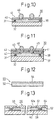
- Figs. 9 and 10 illustrate a further example which falls outside the scope of the present invention.
- Reference numeral 41 denotes an insulation sheet made, for example, of polyimide, epoxy and polyester, and carrying on one surface thereof a circuit pattern 40 made with a copper foil or the like.
- a via-hole 44 is formed at a position on the insulation sheet 41, at which a contact 40a of the circuit pattern 40 to be connected to an external terminal is provided, so that the contact 40a is exposed (see Fig. 9).
- Reference numeral 38 denotes an anisotropic conductive sheet wherein an conductive filler such as a metallic powder is blended in the same manner as described before.
- reference numeral 37 denotes a bump 37 formed on an Al pad of a semiconductor chip 32.
- the semiconductor chip 32, the anisotropic conductive sheet 38 and the insulation sheet 41 are overlapped with each other while disposing one surface of the insulation sheet 41 carrying the circuitpattern 40 opposite to the anisotropic conductive sheet 38, and pressed together to be an integral body.
- the anisotropic conductive sheet 38 is pressed by the bump 37 to electrically connect the circuit pattern 40 at that position with the Al pad.
- a bump 46 is formed as an external terminal in a via-hole 44, and thus a semiconductor device 30 is completed.
- the bump 37 may be formed on the circuit pattern 40.
- connection between the circuit pattern 40 and the Al pad may be easily made via the anisotropic conductive sheet 38.
- the same process as mentioned above can also be applied to a wafer which is provided with a number of chips. In this case, such a wafer is laminated in the same manner as above and cut into individual semiconductor devices.
- a and B are first layered and then laminated with C.
- semiconductor devices according to the present invention can also be obtained by the same process as mentioned above. Namely, such semiconductor devices can be made by laminating the wafer and slicing it into individual devices.
- Fig. 11 illustrates an example wherein insulation sheets 41 carrying circuit patterns 40 thereon are overlapped with a semiconductor chip 32 in a multilayer manner.
- the insulation sheets 41 are bonded to each other with an adhesive 43, and the circuit patterns 40 are electrically connected to each other through vias 45, which can be formed by plating or a conductive resin.
- the lowermost insulation sheet 41 is fixed via an anisotropic conductive sheet 38 while being electrically connected in the same manner as described before.
- an intermediate circuit pattern may be provided for the power supply or the grounding.
- Fig. 12 illustrates an anisotropic conductive sheet 50 with a conductive layer
- the anisotropic conductive sheet 50 is constituted by an anisotropic conductive sheet 52 carrying a conductive layer 54 made of a copper foil or the like on the surface thereof.
- the anisotropic conductive sheet 52 is made of a resin such as epoxy, polyimide or silicone blended with an conductive filler such as a metallic filler or the like. Since the silicone resin has a rubber-like elasticity, it can mitigate a stress particularly generated between a semiconductor chip and a substrate mounting the same.
- the conductive filler may be a metallic powder such as Ni, a metallic powder such as Ag or Ag-Pd; or Ni, Ag or Ag-Pd covered with a resin such as epoxy, polyimide or silicone; or a resin powder such as epoxy, polyimide or silicone covered with a plated metallic film such as Ni, Ag or Ag-Pd, a necessary amount of which is blended into the resin for creating the conductivity when particles of the conductive filler are brought into contact with each other by pressing the sheet.
- the conductive layer 54 may be formed not only by adhering a metallic foil such as a copper foil to the anisotropic conductive sheet 52 but also by forming a metal layer such as copper through a sputtering method or a metallizing method. Or, the conductive layer 54 may be formed in a sheet-like shape by casting, on a metallic foil such as a copper foil, an anisotropic conductive paste prepared by blending an conductive filler with a resin (according to a doctor blade method) and curing the same to result in the anisotropic conductive sheet with a conductive layer.
- the anisotropic conductive sheet 50 with a conductive layer is suitably used for forming not only the semiconductor devices 30 shown in Figs. 1 through 11 but also the following circuit boards.
- Fig. 13 shows one example of such circuit boards 56.
- Reference numeral 58 denotes a circuit board (substrate) carrying a circuit pattern 60 formed of a copper foil or the like by a conventional method.
- Reference numeral 52 denotes an anisotropic conductive sheet carrying, on the surface thereof, a circuit pattern 62 formed by etching the conductive layer 54 of the anisotropic conductive sheet 50 with a conductive layer.
- This anisotropic conductive sheet 52 is bonded to the substrate 58 on the surface opposite to one carrying the circuit pattern 62.
- the electrical connection between the circuit patterns 62 and 60 is made via the anisotropic conductive sheet 52 by pressing portions corresponding to the circuit patterns 62 by a suitable tool (not shown) to deform the same.
- Reference numeral 64 denotes a photosensitive resist film (electro-insulation film) covering the anisotropic conductive sheet 52 and the circuit patterns 62.
- the photosensitive resist film 64 is a protective film for the circuit patterns 62 and may be made of various photosensitive solder resists.
- via-holes 66 are formed (so that a contact 62a in the circuit pattern 62 to which an external terminal is to be connected is exposed from the respective via-hole 66).
- An external electronic element may be connected to the contact 62a by solder or the like.
- the circuit board 56 can have a smaller thickness.
- a silicone resin having a rubber-like elasticity, a stress generated between the circuit board and the external electronic element to be mounted thereon can be mitigated.
- the hardness of the anisotropic conductive sheet 52 and of the photosensitive resist film 64 is not so high, they also function as a shock absorbing layer for protecting the external electronic element to be mounted thereto.
- the anisotropic conductive sheet 52 is used as described above, the electric connection can be easily made between the circuit patterns 60 and 62.
- Fig. 14 illustrates another example of a circuit board 56.
- a bump 61 of Au or the like is formed on a circuit pattern 60 in the same manner as shown in Fig. 3 so that an anisotropic conductive sheet 52 is pressed thereby to electrically connect the circuit pattern 60 to a circuit pattern 62. Since the circuit pattern 62 is maintained generally flat by forming the bump 61 in such a manner, the overlapping of the anisotropic conductive sheet 52 is facilitated.
- Fig. 15 illustrates an embodiment wherein a plurality of anisotropic conductive sheets 52 are overlapped with a printed circuit board 58.
- connection between circuit patterns 62 carried on upper and lower anisotropic conductive sheets 52, respectively, and the connection between the circuit pattern 62 and a circuit pattern 60 may be made via the anisotropic conductive sheets by pressing and deforming the circuit pattern in the same manner as shown in Fig. 13, or by pressing the anisotropic conductive sheets 52 with bumps 61, 61 formed on the circuit patterns 60 and 62 as shown in the drawing.
- the intermediate circuit pattern 62 may be formed as an overall pattern (not shown) for the power supply or the grounding having the same structure as that shown in Fig. 8.
- the wiring of a power supply line in the circuit pattern 62 of the upper layer becomes easy; while, if it is used as the grounding, in addition to the freedom of wiring, the electrical properties are improved because a so-called decoupling capacitor can be formed in the overall pattern by a sputtering method or the like.
- the overall pattern for the power supply or the grounding may be partially provided in portions corresponding to electronic elements to be mounted.
- the printed circuit board may be made of ceramic.
- Fig. 16 illustrates another embodiment of a printed circuit board 56.
- a plurality of (three in the drawing) anisotropic conductive sheets 52 carrying circuit patterns are overlapped.
- a first layer is prepared by an anisotropic conductive sheet 50 having, on both surface thereof, conductive layers which are etched to be circuit patterns 62 and 62a, respectively.
- Each of second and third layers 52 is prepared by an anisotropic conductive sheet having, on one surface thereof, a conductive layer which is etched to be a circuit pattern 62. The three sheets are thermally press-bonded together to form a printed circuit board 56.
- connection between the circuit patterns 62 and 62a in the first layer is made via the anisotropic conductive sheet 52 by pressing and deforming the circuit pattern 62a.
- the connection between the circuit patterns 62 in the first, second and third layers is made via bumps 61 and the anisotropic conductive sheets 52.
- Reference numeral 42 denotes a photosensitive resist film (electro-insulation film) covering the circuit patterns 62 and 62a on the respective surface.
- External terminals 46 such as solder balls are formed in via-holes provided in one of the surfaces, and circuit patterns 62 are exposed through via-holes provided in the other surface so that contacts to be connected to electronic elements are formed.
- the respective circuit pattern 62 may be preliminarily provided in the anisotropic conductive sheet 52 or may be formed by an etching or others every time when the anisotropic conductive sheet with a conductive layer (layers) is overlapped.
- an insulation film 52a of a polyimide sheet, epoxy sheet or an anisotropic conductive sheet carrying a circuit pattern 62 thereon may be used as the first layer, and anisotropic conductive sheets 52 carrying a circuit pattern 62 on one surface thereof as described above may be used as the other layer, which are then overlapped with each other and thermally press-bonded together.
- the bump 46 used as an external terminal may be provided, as shown in Fig. 18, on a metallic layer 33 which is formed in a bottom 40a of the external terminal and around the peripheral edge and the inner wall of the via-hole provided in the electro-insulation sheet 42 or the insulation sheet 41.
- the bonding area of the bump increases to enhance the bonding strength.
Landscapes
- Engineering & Computer Science (AREA)
- Manufacturing & Machinery (AREA)
- Microelectronics & Electronic Packaging (AREA)
- Wire Bonding (AREA)
- Combinations Of Printed Boards (AREA)
- Non-Insulated Conductors (AREA)
Claims (8)
- Leiterplatte (56) mit:einem Substrat (58) mit einer ersten und einer zweiten Fläche, wobei ein erstes Leitungsmuster (60) auf der ersten Fläche des Substrats gebildet ist;einer anisotrop leitenden Lage (52), die wenigstens zwei anisotrope Schichten enthält, die aus einem Basismaterial aus Kunststoff und leitenden Metallpartikeln bestehen, die in dem Basismaterial verteilt sind, wobei jede Schicht eine erste und eine zweite Fläche hat und ein Leitungsmuster (62) auf der ersten Fläche jeder anisotrop leitenden Schicht gebildet ist;wobei wenigstens zwei anisotrop leitende Schichten in der Weise aufeinander laminiert sind, dass die zweite Fläche jeder anisotrop leitenden Schicht an der ersten Fläche der benachbarten anisotrop leitenden Schicht anhaftet;wobei die erste Fläche des Substrats (58) an der zweiten Fläche der untersten anisotrop leitenden Schicht anhaftet;wobei die Leitungsmuster auf den wenigstens zwei anisotrop leitenden Schichten und das Substrat (60,62) elektrisch miteinander über zusammengepresste Abschnitte der mehreren anisotrop leitenden Schichten verbunden sind undeine elektrisch isolierende Schicht (64) auf der ersten Fläche der obersten anisotrop leitenden Schicht ausgebildet ist, um das zweite Leitungsmuster mit Ausnahme von Abschnitten des zweiten Leitungsmusters, die frei bleiben, zu überdecken.
- Leiterplatte (56) nach Anspruch 1,
wobei Vorsprünge (61) auf den Leitungsmustem vorgesehen sind, die auf dem Substrat (60) und jeder anisotrop leitenden Schicht (62) mit Ausnahme der obersten anisotrop leitenden Schicht angeordnet sind, und wobei die anisotrop leitenden Schichten auf den Vorsprüngen laminiert und teilweise von den Vorsprüngen gepresst werden, so dass die gepressten Abschnitte der anisotrop leitenden Schichten elektrisch leitend sind. - Leiterplatte (56) nach Anspruch 1 oder 2,
wobei wenigstens eines der auf dem Substrat und den mehreren anisotrop leitenden Schichten angeordneten Leitungsmuster eine Stromzufuhrleitungsschicht ist, die sich über die gesamte Fläche erstreckt. - Leiterplatte (56) nach jedem der Ansprüche 1 bis 3,
wobei wenigstens eine der auf dem Substrat und den mehreren anisotrop leitenden Schichten angeordneten Leitungsmuster eine Erdungsschicht ist, die sich über die gesamte Fläche erstreckt. - Halbleitervorrichtung (30) mit:einem Halbleiterchip (32) mit einer oberen und einer unteren Fläche, wobei der Chip Elektroden (36) auf der oberen Fläche hat;einem elektrisch isolierenden Film (34) auf der Oberseite des Halbleiterchips mit Ausnahme der Bereiche, an denen sich die Elektroden befinden;mehreren anisotrop leitenden Schichten (38), die jeweils aus einem Basismaterial aus Kunststoff und leitenden Metallpartikeln (39) bestehen, die in dem Basisrnaterial verteilt sind, mit einer oberen und einer unteren Fläche und einem Leitungsmuster (40) auf der oberen Fläche jeder anisotrop leitenden Schicht;wobei die mehreren anisotrop leitenden Schichten (38) miteinander auf solche Weise laminiert sind, dass die Unterseite jeder anisotrop leitenden Schicht an der Oberseite der benachbarten anisotrop leitenden Schicht anhaftet;wobei die Oberseite des Halbleiterchips (32) an der Unterseite der untersten anisotrop leitenden Schicht anhaftet;wobei die Leitungsmuster der mehreren anisotrop leitenden Schichten und die Elektroden des Halbleiterchips über zusammengepresste Abschnitte der mehreren anisotrop leitenden Schichten miteinander elektrisch verbunden sind;eine elektrisch isolierende Schicht (42) auf der Oberseite der obersten anisotrop leitenden Schicht ausgebildet ist, um deren Leitungsmuster mit Ausnahme der äußeren Verbindungsabschnitte (40a), die freibleiben, zu überdecken undäußere Verbindungsanschlüsse (46) an den jeweiligen äußeren Verbindungsabschnitten geformt sind.
- Halbleitervorrichtung (30) nach Anspruch 5,
wobei die unterste anisotrop leitende Schicht zuvor mit Hilfe eines Pressverbindungswerkzeugs (43) an Stellen mechanisch gepresst ist, die den Elektroden entsprechen, so dass die gepressten Abschnitte der untersten anisotrop leitenden Schicht elektrisch leitend sind und damit die Elektroden des Halbleiterchips und die Leitungsmuster der untersten anisotrop leitenden Schicht elektrisch miteinander verbunden sind. - Halbleitervorrichtung (30) nach Anspruch 5,
wobei die Elektroden (36) des Halbleiterchips mit leitenden Vorsprüngen (37) versehen sind, die nach oben über den Isolierfilm vorstehen, so dass die unterste anisotrop leitende Schicht auf den Vorsprüngen laminiert und von den Vorsprüngen teilweise zusammengedrückt sind, womit die gepressten Abschnitte der untersten anisotrop leitenden Schicht elektrisch leitend sind und somit die Elektroden des Halbleiterchips und die Leitungsmuster auf der untersten anisotrop leitenden Schicht elektrisch miteinander verbunden sind. - Halbleitervorrichtung nach jedem der Ansprüche 5 bis 7,
wobei die äußeren Verbindungsanschlüsse (46) Lötmittelvorsprünge sind.
Applications Claiming Priority (3)
| Application Number | Priority Date | Filing Date | Title |
|---|---|---|---|
| JP7613/96 | 1996-01-19 | ||
| JP761396 | 1996-01-19 | ||
| JP00761396A JP3549316B2 (ja) | 1995-03-24 | 1996-01-19 | 配線基板 |
Publications (2)
| Publication Number | Publication Date |
|---|---|
| EP0786808A1 EP0786808A1 (de) | 1997-07-30 |
| EP0786808B1 true EP0786808B1 (de) | 2002-04-10 |
Family
ID=11670672
Family Applications (1)
| Application Number | Title | Priority Date | Filing Date |
|---|---|---|---|
| EP97300275A Expired - Lifetime EP0786808B1 (de) | 1996-01-19 | 1997-01-17 | Gedruckte Schaltungsplatte oder Halbleitervorrichtung mit anisotrop leitenden Platten |
Country Status (4)
| Country | Link |
|---|---|
| US (2) | US5886415A (de) |
| EP (1) | EP0786808B1 (de) |
| KR (1) | KR100274333B1 (de) |
| DE (1) | DE69711735T2 (de) |
Families Citing this family (77)
| Publication number | Priority date | Publication date | Assignee | Title |
|---|---|---|---|---|
| US6111317A (en) * | 1996-01-18 | 2000-08-29 | Kabushiki Kaisha Toshiba | Flip-chip connection type semiconductor integrated circuit device |
| KR100274333B1 (ko) * | 1996-01-19 | 2001-01-15 | 모기 쥰이찌 | 도체층부착 이방성 도전시트 및 이를 사용한 배선기판 |
| US6034437A (en) * | 1997-06-06 | 2000-03-07 | Rohm Co., Ltd. | Semiconductor device having a matrix of bonding pads |
| US6204564B1 (en) | 1997-11-21 | 2001-03-20 | Rohm Co., Ltd. | Semiconductor device and method for making the same |
| US6137063A (en) * | 1998-02-27 | 2000-10-24 | Micron Technology, Inc. | Electrical interconnections |
| JP2000022039A (ja) * | 1998-07-06 | 2000-01-21 | Shinko Electric Ind Co Ltd | 半導体装置及びその製造方法 |
| US6489183B1 (en) * | 1998-07-17 | 2002-12-03 | Micron Technology, Inc. | Method of manufacturing a taped semiconductor device |
| EP1114457B1 (de) | 1998-08-21 | 2010-05-12 | Infineon Technologies AG | Verfahren zur herstellung von integrierten schaltkreisen |
| JP3420706B2 (ja) * | 1998-09-22 | 2003-06-30 | 株式会社東芝 | 半導体装置、半導体装置の製造方法、回路基板、回路基板の製造方法 |
| JP3661444B2 (ja) * | 1998-10-28 | 2005-06-15 | 株式会社ルネサステクノロジ | 半導体装置、半導体ウエハ、半導体モジュールおよび半導体装置の製造方法 |
| JP2000150560A (ja) * | 1998-11-13 | 2000-05-30 | Seiko Epson Corp | バンプ形成方法及びバンプ形成用ボンディングツール、半導体ウエーハ、半導体チップ及び半導体装置並びにこれらの製造方法、回路基板並びに電子機器 |
| JP3502776B2 (ja) * | 1998-11-26 | 2004-03-02 | 新光電気工業株式会社 | バンプ付き金属箔及び回路基板及びこれを用いた半導体装置 |
| JP3530761B2 (ja) | 1999-01-18 | 2004-05-24 | 新光電気工業株式会社 | 半導体装置 |
| US6326701B1 (en) * | 1999-02-24 | 2001-12-04 | Sanyo Electric Co., Ltd. | Chip size package and manufacturing method thereof |
| JP3128548B2 (ja) * | 1999-03-11 | 2001-01-29 | 沖電気工業株式会社 | 半導体装置および半導体装置の製造方法 |
| US6228687B1 (en) | 1999-06-28 | 2001-05-08 | Micron Technology, Inc. | Wafer-level package and methods of fabricating |
| US6239489B1 (en) * | 1999-07-30 | 2001-05-29 | Micron Technology, Inc. | Reinforcement of lead bonding in microelectronics packages |
| KR100347135B1 (ko) * | 1999-12-24 | 2002-07-31 | 주식회사 하이닉스반도체 | 웨이퍼 레벨의 멀티칩 패키지 및 그 제조방법 |
| KR100386637B1 (ko) * | 1999-12-30 | 2003-06-02 | 앰코 테크놀로지 코리아 주식회사 | 반도체 패키지 및 그 제조방법 |
| JP3568869B2 (ja) * | 2000-02-28 | 2004-09-22 | シャープ株式会社 | 半導体集積回路装置及びその製造方法 |
| KR100440507B1 (ko) * | 2000-03-23 | 2004-07-15 | 세이코 엡슨 가부시키가이샤 | 반도체장치 및 그 제조방법, 회로기판 및 전자기기 |
| KR100315158B1 (ko) | 2000-08-02 | 2001-11-26 | 윤덕용 | 비솔더 플립 칩 본딩용 고신뢰성 비전도성 접착제 및 이를이용한 플립 칩 본딩 방법 |
| JP4454814B2 (ja) * | 2000-08-29 | 2010-04-21 | Necエレクトロニクス株式会社 | 樹脂封止型半導体装置及びその製造方法 |
| US6421253B1 (en) | 2000-09-08 | 2002-07-16 | Powerwave Technologies, Inc. | Durable laminated electronics assembly using epoxy preform |
| JP4174174B2 (ja) * | 2000-09-19 | 2008-10-29 | 株式会社ルネサステクノロジ | 半導体装置およびその製造方法並びに半導体装置実装構造体 |
| JP2002118199A (ja) * | 2000-10-10 | 2002-04-19 | Mitsubishi Electric Corp | 半導体装置 |
| KR100398315B1 (ko) * | 2001-02-12 | 2003-09-19 | 한국과학기술원 | 고주파 패키지용 플립 칩 접속을 위한 전도성 접착제의 제조방법 |
| US7498196B2 (en) | 2001-03-30 | 2009-03-03 | Megica Corporation | Structure and manufacturing method of chip scale package |
| KR20020091327A (ko) * | 2001-05-31 | 2002-12-06 | 삼성전자 주식회사 | 측면 몸체부가 형성되어 있는 웨이퍼 레벨 패키지 및 그제조 방법 |
| DE10231385B4 (de) * | 2001-07-10 | 2007-02-22 | Samsung Electronics Co., Ltd., Suwon | Halbleiterchip mit Bondkontaktstellen und zugehörige Mehrchippackung |
| US6555912B1 (en) * | 2001-10-23 | 2003-04-29 | International Business Machines Corporation | Corrosion-resistant electrode structure for integrated circuit decoupling capacitors |
| JP2003152014A (ja) * | 2001-11-09 | 2003-05-23 | Shinko Electric Ind Co Ltd | 半導体装置の製造方法及び半導体装置 |
| TW517361B (en) * | 2001-12-31 | 2003-01-11 | Megic Corp | Chip package structure and its manufacture process |
| TW503496B (en) | 2001-12-31 | 2002-09-21 | Megic Corp | Chip packaging structure and manufacturing process of the same |
| US6673698B1 (en) * | 2002-01-19 | 2004-01-06 | Megic Corporation | Thin film semiconductor package utilizing a glass substrate with composite polymer/metal interconnect layers |
| TW544882B (en) * | 2001-12-31 | 2003-08-01 | Megic Corp | Chip package structure and process thereof |
| TW584950B (en) | 2001-12-31 | 2004-04-21 | Megic Corp | Chip packaging structure and process thereof |
| DE10202881B4 (de) * | 2002-01-25 | 2007-09-20 | Infineon Technologies Ag | Verfahren zur Herstellung von Halbleiterchips mit einer Chipkantenschutzschicht, insondere für Wafer Level Packaging Chips |
| AU2003220941A1 (en) * | 2002-03-20 | 2003-09-29 | J.S.T. Mfg. Co., Ltd. | Flexible good conductive layer and anisotropic conductive sheet comprising same |
| US7423336B2 (en) * | 2002-04-08 | 2008-09-09 | Micron Technology, Inc. | Bond pad rerouting element, rerouted semiconductor devices including the rerouting element, and assemblies including the rerouted semiconductor devices |
| US7579681B2 (en) * | 2002-06-11 | 2009-08-25 | Micron Technology, Inc. | Super high density module with integrated wafer level packages |
| KR100481216B1 (ko) * | 2002-06-07 | 2005-04-08 | 엘지전자 주식회사 | 볼 그리드 어레이 패키지 및 그의 제조 방법 |
| JP2004193334A (ja) * | 2002-12-11 | 2004-07-08 | Senju Metal Ind Co Ltd | バンプ形成用シートおよびその製造方法 |
| US20040176855A1 (en) * | 2003-03-07 | 2004-09-09 | Acell, Inc. | Decellularized liver for repair of tissue and treatment of organ deficiency |
| US7701069B2 (en) * | 2003-06-30 | 2010-04-20 | Intel Corporation | Solder interface locking using unidirectional growth of an intermetallic compound |
| US7084053B2 (en) * | 2003-09-30 | 2006-08-01 | Intel Corporation | Unidirectionally conductive materials for interconnection |
| FR2863767B1 (fr) * | 2003-12-12 | 2006-06-09 | Commissariat Energie Atomique | Support memoire irreversible a deformation plastique et procede de realisation d'un tel support |
| JP2005347353A (ja) | 2004-05-31 | 2005-12-15 | Sanyo Electric Co Ltd | 回路装置およびその製造方法 |
| TWI260039B (en) * | 2005-06-17 | 2006-08-11 | Phoenix Prec Technology Corp | Wafer and single chip with circuit rearranged structure and method for fabricating the same |
| KR100664310B1 (ko) * | 2005-07-13 | 2007-01-04 | 삼성전자주식회사 | 웨이퍼 레벨 인캡슐레이션 칩 및 인캡슐레이션 칩 제조방법 |
| JP2007208568A (ja) * | 2006-01-31 | 2007-08-16 | Nippon Dempa Kogyo Co Ltd | 表面実装水晶発振器 |
| JP2008042077A (ja) * | 2006-08-09 | 2008-02-21 | Renesas Technology Corp | 半導体装置及びその製造方法 |
| US9894771B2 (en) * | 2007-05-08 | 2018-02-13 | Joseph Charles Fjelstad | Occam process for components having variations in part dimensions |
| US7713861B2 (en) * | 2007-10-13 | 2010-05-11 | Wan-Ling Yu | Method of forming metallic bump and seal for semiconductor device |
| KR100973268B1 (ko) | 2008-03-07 | 2010-07-30 | 주식회사 하이닉스반도체 | 인쇄회로기판 및 그의 제조방법 |
| JP5481928B2 (ja) * | 2009-05-19 | 2014-04-23 | 株式会社リコー | 配線層レイアウト方法及び半導体装置 |
| US8368153B2 (en) * | 2010-04-08 | 2013-02-05 | United Microelectronics Corp. | Wafer level package of MEMS microphone and manufacturing method thereof |
| JP5435493B2 (ja) * | 2010-06-22 | 2014-03-05 | 富士フイルム株式会社 | 微細構造体およびその製造方法 |
| KR102268781B1 (ko) * | 2014-11-12 | 2021-06-28 | 삼성전자주식회사 | 인쇄회로기판 및 이를 포함하는 반도체 패키지 |
| US11069734B2 (en) | 2014-12-11 | 2021-07-20 | Invensas Corporation | Image sensor device |
| US9484227B1 (en) * | 2015-06-22 | 2016-11-01 | Taiwan Semiconductor Manufacturing Company, Ltd. | Dicing in wafer level package |
| US9741620B2 (en) | 2015-06-24 | 2017-08-22 | Invensas Corporation | Structures and methods for reliable packages |
| US10446532B2 (en) | 2016-01-13 | 2019-10-15 | Invensas Bonding Technologies, Inc. | Systems and methods for efficient transfer of semiconductor elements |
| JP6863363B2 (ja) * | 2016-03-08 | 2021-04-21 | 東洋紡株式会社 | 伸縮性導体シート、接着性のある伸縮性導体シート、布帛上への伸縮性導体からなる配線の形成方法 |
| US10204893B2 (en) * | 2016-05-19 | 2019-02-12 | Invensas Bonding Technologies, Inc. | Stacked dies and methods for forming bonded structures |
| US10120971B2 (en) * | 2016-08-30 | 2018-11-06 | Taiwan Semiconductor Manufacturing Co., Ltd. | Integrated fan-out package and layout method thereof |
| US10879212B2 (en) | 2017-05-11 | 2020-12-29 | Invensas Bonding Technologies, Inc. | Processed stacked dies |
| US10217720B2 (en) | 2017-06-15 | 2019-02-26 | Invensas Corporation | Multi-chip modules formed using wafer-level processing of a reconstitute wafer |
| US11276676B2 (en) | 2018-05-15 | 2022-03-15 | Invensas Bonding Technologies, Inc. | Stacked devices and methods of fabrication |
| WO2020010265A1 (en) | 2018-07-06 | 2020-01-09 | Invensas Bonding Technologies, Inc. | Microelectronic assemblies |
| US11158606B2 (en) | 2018-07-06 | 2021-10-26 | Invensas Bonding Technologies, Inc. | Molded direct bonded and interconnected stack |
| CN113330557A (zh) | 2019-01-14 | 2021-08-31 | 伊文萨思粘合技术公司 | 键合结构 |
| US11296053B2 (en) | 2019-06-26 | 2022-04-05 | Invensas Bonding Technologies, Inc. | Direct bonded stack structures for increased reliability and improved yield in microelectronics |
| US12080672B2 (en) | 2019-09-26 | 2024-09-03 | Adeia Semiconductor Bonding Technologies Inc. | Direct gang bonding methods including directly bonding first element to second element to form bonded structure without adhesive |
| US11631647B2 (en) | 2020-06-30 | 2023-04-18 | Adeia Semiconductor Bonding Technologies Inc. | Integrated device packages with integrated device die and dummy element |
| US11764177B2 (en) | 2020-09-04 | 2023-09-19 | Adeia Semiconductor Bonding Technologies Inc. | Bonded structure with interconnect structure |
| US11728273B2 (en) | 2020-09-04 | 2023-08-15 | Adeia Semiconductor Bonding Technologies Inc. | Bonded structure with interconnect structure |
Citations (1)
| Publication number | Priority date | Publication date | Assignee | Title |
|---|---|---|---|---|
| EP0734065A2 (de) * | 1995-03-24 | 1996-09-25 | Shinko Electric Industries Co. Ltd. | Halbleiteranordnung in Chipgrösse |
Family Cites Families (16)
| Publication number | Priority date | Publication date | Assignee | Title |
|---|---|---|---|---|
| US3832769A (en) * | 1971-05-26 | 1974-09-03 | Minnesota Mining & Mfg | Circuitry and method |
| US4249302A (en) * | 1978-12-28 | 1981-02-10 | Ncr Corporation | Multilayer printed circuit board |
| US4811081A (en) * | 1987-03-23 | 1989-03-07 | Motorola, Inc. | Semiconductor die bonding with conductive adhesive |
| JPS63291493A (ja) * | 1987-05-22 | 1988-11-29 | Sharp Corp | 回路パタ−ンのジャンパ−接続方法 |
| GB2218586A (en) * | 1988-05-11 | 1989-11-15 | Plessey Co Plc | Improved stability crystal oscillator |
| US5502889A (en) * | 1988-06-10 | 1996-04-02 | Sheldahl, Inc. | Method for electrically and mechanically connecting at least two conductive layers |
| US5010038A (en) * | 1989-06-29 | 1991-04-23 | Digital Equipment Corp. | Method of cooling and powering an integrated circuit chip using a compliant interposing pad |
| JP2785441B2 (ja) * | 1990-05-11 | 1998-08-13 | ソニー株式会社 | 半導体装置とその製造方法 |
| US5225966A (en) * | 1991-07-24 | 1993-07-06 | At&T Bell Laboratories | Conductive adhesive film techniques |
| US5259110A (en) * | 1992-04-03 | 1993-11-09 | International Business Machines Corporation | Method for forming a multilayer microelectronic wiring module |
| JP2785575B2 (ja) * | 1992-04-08 | 1998-08-13 | 日本電気株式会社 | Ic内蔵型蛍光表示管とその製造方法 |
| JP2601128B2 (ja) * | 1992-05-06 | 1997-04-16 | 松下電器産業株式会社 | 回路形成用基板の製造方法および回路形成用基板 |
| JPH0677280A (ja) * | 1992-08-24 | 1994-03-18 | Sumitomo Electric Ind Ltd | 半導体素子の実装方法 |
| JPH06283776A (ja) * | 1993-03-26 | 1994-10-07 | Brother Ind Ltd | 積層型圧電素子 |
| JPH07201864A (ja) * | 1993-12-28 | 1995-08-04 | Fujitsu Ltd | 突起電極形成方法 |
| KR100274333B1 (ko) * | 1996-01-19 | 2001-01-15 | 모기 쥰이찌 | 도체층부착 이방성 도전시트 및 이를 사용한 배선기판 |
-
1997
- 1997-01-15 KR KR1019970000992A patent/KR100274333B1/ko not_active Expired - Fee Related
- 1997-01-17 US US08/786,615 patent/US5886415A/en not_active Expired - Lifetime
- 1997-01-17 DE DE69711735T patent/DE69711735T2/de not_active Expired - Lifetime
- 1997-01-17 EP EP97300275A patent/EP0786808B1/de not_active Expired - Lifetime
-
1998
- 1998-10-08 US US09/168,148 patent/US6121688A/en not_active Expired - Lifetime
Patent Citations (1)
| Publication number | Priority date | Publication date | Assignee | Title |
|---|---|---|---|---|
| EP0734065A2 (de) * | 1995-03-24 | 1996-09-25 | Shinko Electric Industries Co. Ltd. | Halbleiteranordnung in Chipgrösse |
Also Published As
| Publication number | Publication date |
|---|---|
| DE69711735T2 (de) | 2002-11-21 |
| KR100274333B1 (ko) | 2001-01-15 |
| DE69711735D1 (de) | 2002-05-16 |
| US5886415A (en) | 1999-03-23 |
| KR970061017A (ko) | 1997-08-12 |
| US6121688A (en) | 2000-09-19 |
| EP0786808A1 (de) | 1997-07-30 |
Similar Documents
| Publication | Publication Date | Title |
|---|---|---|
| EP0786808B1 (de) | Gedruckte Schaltungsplatte oder Halbleitervorrichtung mit anisotrop leitenden Platten | |
| EP0734065B1 (de) | Halbleiteranordnung in der Grösse eines oder mehrerer Chips | |
| JP3502776B2 (ja) | バンプ付き金属箔及び回路基板及びこれを用いた半導体装置 | |
| US6395582B1 (en) | Methods for forming ground vias in semiconductor packages | |
| US5858815A (en) | Semiconductor package and method for fabricating the same | |
| JP2570499B2 (ja) | フリップチップ集積回路の背面接地 | |
| JP4606849B2 (ja) | デカップリングコンデンサを有する半導体チップパッケージ及びその製造方法 | |
| US5147210A (en) | Polymer film interconnect | |
| JP3176307B2 (ja) | 集積回路装置の実装構造およびその製造方法 | |
| US6147311A (en) | Multi layer circuit board using anisotropic electroconductive adhesive layer and method for producing same | |
| US6952047B2 (en) | Assemblies having stacked semiconductor chips and methods of making same | |
| US20080230892A1 (en) | Chip package module | |
| WO2000070677A1 (en) | Semiconductor device, method of manufacture thereof, circuit board, and electronic device | |
| US6448509B1 (en) | Printed circuit board with heat spreader and method of making | |
| JPH06120670A (ja) | 多層配線基板 | |
| US6034437A (en) | Semiconductor device having a matrix of bonding pads | |
| JP2001168233A (ja) | 多重回線グリッド・アレイ・パッケージ | |
| JP3569585B2 (ja) | 半導体装置 | |
| US20040256715A1 (en) | Wiring board, semiconductor device and process of fabricating wiring board | |
| JP3549316B2 (ja) | 配線基板 | |
| US20020063331A1 (en) | Film carrier semiconductor device | |
| JP3378171B2 (ja) | 半導体パッケージの製造方法 | |
| US7239024B2 (en) | Semiconductor package with recess for die | |
| JP2722451B2 (ja) | 半導体装置 | |
| JP3841135B2 (ja) | 半導体装置、回路基板及び電子機器 |
Legal Events
| Date | Code | Title | Description |
|---|---|---|---|
| PUAI | Public reference made under article 153(3) epc to a published international application that has entered the european phase |
Free format text: ORIGINAL CODE: 0009012 |
|
| AK | Designated contracting states |
Kind code of ref document: A1 Designated state(s): DE FR GB |
|
| 17P | Request for examination filed |
Effective date: 19980116 |
|
| 17Q | First examination report despatched |
Effective date: 19990507 |
|
| GRAG | Despatch of communication of intention to grant |
Free format text: ORIGINAL CODE: EPIDOS AGRA |
|
| RTI1 | Title (correction) |
Free format text: PRINTED CIRCUIT BOARD OR SEMICONDUCTOR DEVICE COMPRISING ANISOTROPIC CONDUCTIVE SHEETS |
|
| GRAG | Despatch of communication of intention to grant |
Free format text: ORIGINAL CODE: EPIDOS AGRA |
|
| GRAH | Despatch of communication of intention to grant a patent |
Free format text: ORIGINAL CODE: EPIDOS IGRA |
|
| REG | Reference to a national code |
Ref country code: GB Ref legal event code: IF02 |
|
| GRAH | Despatch of communication of intention to grant a patent |
Free format text: ORIGINAL CODE: EPIDOS IGRA |
|
| GRAA | (expected) grant |
Free format text: ORIGINAL CODE: 0009210 |
|
| AK | Designated contracting states |
Kind code of ref document: B1 Designated state(s): DE FR GB |
|
| REF | Corresponds to: |
Ref document number: 69711735 Country of ref document: DE Date of ref document: 20020516 |
|
| ET | Fr: translation filed | ||
| PLBE | No opposition filed within time limit |
Free format text: ORIGINAL CODE: 0009261 |
|
| STAA | Information on the status of an ep patent application or granted ep patent |
Free format text: STATUS: NO OPPOSITION FILED WITHIN TIME LIMIT |
|
| 26N | No opposition filed |
Effective date: 20030113 |
|
| REG | Reference to a national code |
Ref country code: FR Ref legal event code: PLFP Year of fee payment: 19 |
|
| PGFP | Annual fee paid to national office [announced via postgrant information from national office to epo] |
Ref country code: DE Payment date: 20150113 Year of fee payment: 19 |
|
| PGFP | Annual fee paid to national office [announced via postgrant information from national office to epo] |
Ref country code: FR Payment date: 20150108 Year of fee payment: 19 Ref country code: GB Payment date: 20150114 Year of fee payment: 19 |
|
| REG | Reference to a national code |
Ref country code: DE Ref legal event code: R119 Ref document number: 69711735 Country of ref document: DE |
|
| GBPC | Gb: european patent ceased through non-payment of renewal fee |
Effective date: 20160117 |
|
| REG | Reference to a national code |
Ref country code: FR Ref legal event code: ST Effective date: 20160930 |
|
| PG25 | Lapsed in a contracting state [announced via postgrant information from national office to epo] |
Ref country code: GB Free format text: LAPSE BECAUSE OF NON-PAYMENT OF DUE FEES Effective date: 20160117 Ref country code: DE Free format text: LAPSE BECAUSE OF NON-PAYMENT OF DUE FEES Effective date: 20160802 |
|
| PG25 | Lapsed in a contracting state [announced via postgrant information from national office to epo] |
Ref country code: FR Free format text: LAPSE BECAUSE OF NON-PAYMENT OF DUE FEES Effective date: 20160201 |