EP0786873B1 - Radioémetteur-récepteur avec un amplificateur à fonctionnement séquentiel - Google Patents
Radioémetteur-récepteur avec un amplificateur à fonctionnement séquentiel Download PDFInfo
- Publication number
- EP0786873B1 EP0786873B1 EP97300395A EP97300395A EP0786873B1 EP 0786873 B1 EP0786873 B1 EP 0786873B1 EP 97300395 A EP97300395 A EP 97300395A EP 97300395 A EP97300395 A EP 97300395A EP 0786873 B1 EP0786873 B1 EP 0786873B1
- Authority
- EP
- European Patent Office
- Prior art keywords
- carrier
- coupled
- amplifiers
- transceiver
- amplifier
- Prior art date
- Legal status (The legal status is an assumption and is not a legal conclusion. Google has not performed a legal analysis and makes no representation as to the accuracy of the status listed.)
- Expired - Lifetime
Links
- 230000005540 biological transmission Effects 0.000 claims description 13
- 230000010363 phase shift Effects 0.000 claims description 7
- 230000008878 coupling Effects 0.000 claims description 5
- 238000010168 coupling process Methods 0.000 claims description 5
- 238000005859 coupling reaction Methods 0.000 claims description 5
- 230000010355 oscillation Effects 0.000 claims description 3
- 230000003213 activating effect Effects 0.000 claims 1
- 238000010586 diagram Methods 0.000 description 4
- 238000010897 surface acoustic wave method Methods 0.000 description 2
- 230000001627 detrimental effect Effects 0.000 description 1
- 230000004048 modification Effects 0.000 description 1
- 238000012986 modification Methods 0.000 description 1
- 230000005855 radiation Effects 0.000 description 1
Images
Classifications
-
- H—ELECTRICITY
- H04—ELECTRIC COMMUNICATION TECHNIQUE
- H04B—TRANSMISSION
- H04B1/00—Details of transmission systems, not covered by a single one of groups H04B3/00 - H04B13/00; Details of transmission systems not characterised by the medium used for transmission
- H04B1/38—Transceivers, i.e. devices in which transmitter and receiver form a structural unit and in which at least one part is used for functions of transmitting and receiving
- H04B1/40—Circuits
Definitions
- the present invention relates in general to transceivers and in particular to a transceiver in which the receiver portion utilizes a sequential amplifier and in which the transmitter uses a portion of the circuitry in the receiver so as to reduce the number of components required in the transceiver circuit.
- Transmitter receivers are old and well known in the art. They comprise generally a receiver and a transmitter and a transmit/receive control that enables the transmitter and disables the receiver during transmission.
- the second amplifier Prior to, or at least about the time the signal emerges from the delay line, as the signal reaches the second stage amplifier, the second amplifier will be energized and the first amplifier will be substantially de-energized. In the second stage amplifier, the signal will again be amplified. The first stage amplifier will be switched OFF when the second stage amplifier is switched ON and vice versa.
- the voltage controlled oscillator has an amplifier coupled in series with a SAW coupled resonator.
- the SAW coupled resonator may be replaced with a delay line surface acoustic wave device.
- U.S. Patent No. 4,761,616 discloses a voltage controlled oscillator which uses a SAW device in the feedback loop and the SAW device can be a delay line
- U.S. Patent No. 5,357,206 requires a delay line between sequential amplifier stages, it would be advantageous to combine the two circuits such that the delay line between the sequential amplifiers in the receiver stage could be used during transmission to form an oscillator for generating the carrier frequency for the transmitter.
- the present invention combines elements in the receiver with elements in the transmitter such that during transmission, certain of the elements in the receiver are used as a part of the transmitter.
- the delay line that couples first and second RF stages in the sequential amplifier is used with a third RF amplifier when the unit is transmitting to form an oscillator for generating the transmitter carrier frequency.
- a transmit control circuit can be used to disable the first and second RF amplifiers in the receiver and enable the third and fourth RF amplifiers in the transmitter to generate oscillator carrier signals that are to be modulated with data. For instance, the transmit control circuit may amplitude modulate the oscillator carrier signals that are being transmitted. Thus, the transmit control circuit may turn ON and OFF the third and fourth RF amplifiers in the transmitter to provide on-and-off key (OOK) amplitude modulation according to the data applied thereto.
- OOK on-and-off key
- a frequency modulation circuit is coupled between the delay line and the third RF amplifier forming the oscillator circuit. Data is supplied to the frequency modulation circuit to frequency modulate (FM) the oscillator carrier signals.
- a transmit control circuit turns ON the third and fourth amplifier stages to couple the frequency modulated RF signals to an antenna.
- the FM circuit frequency shift key (FSK) modulates the oscillator carrier signal with the data.
- phase-shift modulator (PSM) circuit may be coupled between the output or fourth amplifier in the transmitter and the antenna.
- a transmit control circuit can turn ON the third and fourth RF amplifiers in the transmitter to couple the oscillator carrier frequency to the phase modulation circuit.
- Data can then be supplied to the phase modulation circuit for phase modulating the carrier frequency coupled to the antenna.
- the phase modulation circuit may be used to phase shift key modulate (PSKM) the oscillator carrier signal with the data.
- a transceiver in which a receiver circuit is formed of first and second series coupled RF amplifier stages being coupled to each other by a delay line.
- the first RF amplifier is coupled to the antenna for receiving RF signals.
- a receiver control circuit is coupled to the first and second RF amplifiers for turning OFF both said first and second RF amplifiers simultaneously during transmission and for sequentially turning ON and OFF said first and second RF amplifiers when receiving RF signals.
- the delay line prevents the first and second RF amplifiers from oscillating. This is the circuit disclosed in U.S. Patent No. 5,357,206.
- a demodulator is coupled to the second RF amplifier for receiving the amplified and RF signals therefrom and demodulating the signals to generate output data.
- the transmitting circuit includes third and fourth series coupled RF amplifiers having sufficiently low gain so as to prevent oscillation between them.
- the delay line of the receiver is coupled across the third RF amplifier to form a delay line oscillator as disclosed in U.S. Patent No. 4,761,616 for generating an oscillator carrier signal.
- the fourth RF amplifier has an input for receiving the oscillator carrier signals and an output for coupling the oscillator carrier signals to the antenna.
- a transmit control circuit is coupled to the third and fourth RF amplifiers to enable the oscillator carrier signal to be modulated with data.
- a transmit/receive switch is coupled to the receiver control circuit and to the transmitter control circuit for selectively enabling either the transmission or the reception of RF signals.
- It still another object of the present invention to phase shift key modulate the oscillator carrier signal with said data in said phase modulation circuit.
- the present invention relates to a transceiver including a receiver circuit and a transmitting circuit both of which are coupled to an antenna.
- the receiver circuit includes first and second series coupled RF amplifiers coupled to each other by a delay line.
- the first RF amplifier is coupled to the antenna for receiving RF signals.
- a receiver control circuit is coupled to the first and second RF amplifiers for turning OFF both the first and second RF amplifiers simultaneously during transmission and sequentially turning ON and OFF the first and second RF amplifiers when receiving RF signals.
- the delay line prevents the first and second RF amplifiers from oscillating.
- a demodulator is coupled to the second RF amplifier for receiving the amplified RF signal and demodulating the signal to generate output data.
- the transmitting circuit includes third and fourth series coupled RF amplifiers having sufficiently low gain so as to prevent oscillation between them.
- the delay line of the receiver is coupled across the third RF amplifier to form a delay line oscillator for generating oscillator carrier signals.
- the fourth RF amplifier has an input for receiving the oscillator carrier signals and an output for coupling the oscillator carrier signals to the antenna.
- a transmit control circuit is coupled to the third and fourth RF amplifiers to enable the oscillator carrier signals to be modulated with data.
- a transmit/receive switch is coupled to the receiver control circuit and to the transmit control circuit for selectively enabling either the transmission or the reception of RF signals.
- the entire receiver and transmitter may be formed of a single integrated circuit with the SAW delay line being attached to the integrated circuit to form the transceiver.
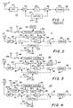
- FIG. 1 illustrates the sequential amplifier receiver as disclosed in U.S. Patent No. 5,357,206 or Patent No. 5,357,207.
- the sequential amplifier 10 includes an antenna 12 coupled to a band-pass filter 14 whose output serves as the input to RF amplifier 16.
- a second RF amplifier 18 is coupled to RF amplifier 16 through a delay line 20.
- a control circuit 22 is enabled by a receive switch signal 24 and alternately enables amplifiers 16 and 18. When amplifier 16 is enabled, amplifier 18 is substantially disabled. The amplifier 16 amplifies the received signal and couples it to delay line 20. As the signal substantially emerges from delay line 20, amplifier 16 is disabled and amplifier 18 enabled by the control circuit 22. The amplified signal is detected with demodulator 26 and the detected output is generated on line 28.
- FIGS. 2, 3, and 4 The novel transceiver of the present invention is illustrated in FIGS. 2, 3, and 4, with FIG. 2 illustrating an amplitude modulation transceiver, FIG. 3 illustrating a frequency modulation transceiver, and FIG. 4 illustrating a phase modulation transceiver.
- FIG. 2 the portions of the receiver that are not utilized during transmission are shown in phantom lines.
- the two amplifiers 16 and 18 and their control unit 22 along with demodulator 26 are unused.
- the antenna 12, the band-pass filter 14, and the delay line 20, all used in the receiver circuit are also used in the transmitter circuit.
- amplifiers 16 and 18 may be referred to as first and second amplifiers that are used in the receiver.
- Amplifiers 32 and 34 in the transmitter circuit may be designated as third and fourth amplifiers.
- the delay line 20 which is also common to the receiver circuit as indicated above, is coupled across the third RF amplifier 32 to form a delay line oscillator as disclosed in U.S. Patent No. 4,761,616 and generates oscillator carrier signals.
- the fourth RF amplifier 34 has an input on line 38 for receiving the oscillator carrier signals and an output on line 40 for coupling the oscillating carrier signals to the antenna 12 through band-pass filter 14.
- Transmit control circuit 44 is coupled to the third and fourth RF amplifiers 32 and 34 to enable the oscillator carrier signals to be modulated with data.
- the data at 42 is coupled to the transmit control 44 and, when transmit switch 46 is closed coupling power from terminal 48 to the control 44, the transmitter control circuit 44 amplitude modulates the oscillator carrier signals that are being transmitted. The amplitude modulation is accomplished in any well-known manner.
- the transmit switch 46 is open and the transmission circuit is disabled.
- the receive switch 30 is open and the receiver portion of the transceiver is disabled.
- FIG. 3 is a circuit similar to that shown in FIG. 2 except that the transceiver 50 includes a transmitter that frequency modulates the carrier.
- the frequency modulation circuit 52 is coupled between the delay line 20 and the third RF amplifier 32.
- the data 54 is coupled to the frequency modulator circuit 52 to modulate the oscillator carrier frequency established by the delay line 20 coupled across the third RF amplifier 32.
- the frequency modulation circuit is old and well known in the art and may frequency shift key modulate the oscillator carrier signal with the data 54.
- the FM circuit 52 is old and well known in the art and need not be discussed in detail here.
- FIG. 4 discloses a transceiver 56 in which a phase modulation circuit 58 is coupled between the fourth RF amplifier 34 and the band pass filter 14.
- the transmit control circuit 44 when energized by closure of the transmission switch 46, turns ON the third and fourth RF amplifiers 32 and 34 to establish the carrier frequency and to amplify the carrier with amplifier 34 and couple it on line 40 to the phase modulation circuit 58 where data on line 60 is used to phase modulate the carrier.
- phase modulation circuits 58 are old and well known in the art and are not discussed in detail here.
- the phase modulation circuit may be a well-known phase shift key modulator to modulate the oscillator carrier signal with the data. Again, phase shift key circuits are old and well known in the art.
- the delay line 20 may be a surface acoustic wave device as disclosed in U.S. Patent No. 4,761,616. Further, in each of the circuits shown in FIGS. 2, 3, and 4, all of the elements, except the delay line and the bandpass filter, may be formed as a single integrated circuit. The delay line may then be attached to the integrated circuit in the correct electrical configuration shown to form the novel transceiver.
- a sequential amplifier is used as the receiver having at least first and second RF amplifier stages connected together with a delay line and wherein the delay line is common to both the receiver and the transmitting circuit.
- the delay line is coupled across an amplifier in the transmitter circuit to form an oscillator that generates the carrier signal.
- the carrier signal may be modulated with AM, on-and-off key amplitude modulation, frequency modulation, frequency shift key modulation, phase modulation, or phase shift key modulation.
- the carrier could be modulated in any manner desired.
Landscapes
- Engineering & Computer Science (AREA)
- Computer Networks & Wireless Communication (AREA)
- Signal Processing (AREA)
- Transceivers (AREA)
- Circuits Of Receivers In General (AREA)
Claims (10)
- Emetteur/récepteur (11) comprenant:une antenne (12);un récepteur comprenant un amplificateur séquentiel couplé à l'antenne (12) pour amplifier une première porteuse RF reçue modulée, l'amplificateur séquentiel comprenant des premier et deuxième amplificateurs (16, 18) RF couplés mutuellement par une ligne (20) à retard;un démodulateur (26) couplé à l'amplificateur séquentiel pour détecter des données dans la première porteuse RF reçue modulée;un émetteur comprenant un oscillateur pour engendrer une deuxième porteuse RF, l'oscillateur comprenant la ligne (20) à retard comme élément de déphasage;un modulateur couplé à l'oscillateur pour moduler la deuxième porteuse RF pour transmission par l'antenne (12); etdes moyens (30, 46) de commutation couplés au récepteur et à l'émetteur pour activer sélectivement l'un ou l'autre du récepteur et de l'émetteur.
- Emetteur/récepteur (11) suivant la revendication 1, comprenant en outre:dans lequel l'émetteur comprend en outre, des troisième et quatrième amplificateurs (32, 34) RF couplés en série ayant un gain suffisamment petit de manière à empêcher une oscillation entre eux, la ligne (20) à retard étant couplée aux bornes du troisième amplificateur (32) RF pour former un oscillateur à ligne (20) à retard pour engendrer la deuxième porteuse RF pour une transmission, le quatrième amplificateur RF ayant une entrée pour recevoir la deuxième porteuse RF et une sortie pour coupler la deuxième porteuse RF à l'antenne (12), et l'émetteur comprenant, en outre, un circuit (44) de contrôle d'émission couplé au troisième et au quatrième amplificateurs RF pour permettre à la deuxième porteuse RF d'être modulée par des données.un circuit (22) de commande du récepteur couplé au premier et au deuxième amplificateurs (16, 18) RF pour mettre hors circuit à la fois le premier et le deuxième amplificateurs (16, 18) RF simultanément pendant une transmission et pour mettre séquentiellement en circuit et hors circuit le premier et le deuxième amplificateurs (16, 18) RF lors de la réception de la première porteuse RF modulée, la ligne (20) à retard empêchant les premier et deuxième amplificateurs (16, 18) RF d'osciller,
- Emetteur/récepteur (11) suivant la revendication 2, comprenant en outre:le circuit (40) de commande d'émission recevant des données; etle circuit (44) de commande d'émission modulant en amplitude la deuxième porteuse RF, qui est émise.
- Emetteur/récepteur (11) suivant la revendication 2 ou la revendication 3, comprenant en outre, le circuit (44) de commande d'émission mettant en circuit et hors circuit les troisième et quatrième amplificateurs (32, 34) RF pour fournir une modulation d'amplitude par tout ou rien (OOK).
- Emetteur/récepteur (11) suivant l'une quelconque des revendications 1 à 4, comprenant en outre:un circuit de modulation de fréquence (FM) couplé entre la ligne (20) à retard et le troisième amplificateur (32) RF;une borne d'entrée pour envoyer des données au circuit de modulation de fréquence pour moduler la fréquence de la deuxième porteuse RF; etle circuit (44) de commande d'émission mettant en circuit les troisième et quatrième amplificateurs (32, 34) RF pour engendrer et coupler la deuxième porteuse RF modulée en fréquence à l'antenne (12).
- Emetteur/récepteur (11) suivant la revendication 5, dans lequel le déphaseur (FSK) de fréquence du circuit (FM) module la deuxième porteuse RF par les données.
- Emetteur/récepteur (11) suivant la revendication l'une quelconque des revendications 2 à 6, comprenant en outre:un circuit de modulation (PM) de phase couplé entre le quatrième amplificateur RF et l'antenne (12);le circuit (44) de commande d'émission mettant en circuit les troisième et quatrième amplificateurs (32, 34) RF pour engendrer et coupler la deuxième porteuse RF au circuit de modulation de phase; etune borne d'entrée pour envoyer des données au circuit de modulation de phase pour moduler en phase la deuxième porteuse RF couplée à l'antenne (12).
- Emetteur/récepteur (11) suivant l'une quelconque des revendications 2 à 7, dans lequel le déphasage (PSK) du circuit de modulation de phase module la deuxième porteuse RF par les données.
- Emetteur/récepteur (11) suivant l'une quelconque des revendications 2 à 8, comprenant en outre un filtre à bande passante couplé entre l'antenne (12) et les premier et quatrième amplificateurs (16, 34) RF pour filtrer des signaux qui sont à la fois émis et reçus.
- Emetteur/récepteur (11) suivant l'une quelconque des revendications précédentes, comprenant en outre:un circuit intégré unique comprenant à la fois l'émetteur et le récepteur; etla ligne (20) à retard étant fixée au circuit intégré pour former l'émetteur (11).
Applications Claiming Priority (2)
| Application Number | Priority Date | Filing Date | Title |
|---|---|---|---|
| US08/592,287 US5787117A (en) | 1996-01-26 | 1996-01-26 | Receiver/transmitter having common elements |
| US592287 | 2000-06-12 |
Publications (3)
| Publication Number | Publication Date |
|---|---|
| EP0786873A2 EP0786873A2 (fr) | 1997-07-30 |
| EP0786873A3 EP0786873A3 (fr) | 1999-09-15 |
| EP0786873B1 true EP0786873B1 (fr) | 2005-05-04 |
Family
ID=24370087
Family Applications (1)
| Application Number | Title | Priority Date | Filing Date |
|---|---|---|---|
| EP97300395A Expired - Lifetime EP0786873B1 (fr) | 1996-01-26 | 1997-01-22 | Radioémetteur-récepteur avec un amplificateur à fonctionnement séquentiel |
Country Status (6)
| Country | Link |
|---|---|
| US (1) | US5787117A (fr) |
| EP (1) | EP0786873B1 (fr) |
| JP (1) | JP3889101B2 (fr) |
| CA (1) | CA2194621C (fr) |
| DE (1) | DE69733163T2 (fr) |
| TW (1) | TW312062B (fr) |
Families Citing this family (12)
| Publication number | Priority date | Publication date | Assignee | Title |
|---|---|---|---|---|
| US6178208B1 (en) * | 1997-12-18 | 2001-01-23 | Legerity | System for recovery of digital data from amplitude and phase modulated line signals using delay lines |
| US6160856A (en) * | 1997-12-18 | 2000-12-12 | Advanced Micro Devices, Inc. | System for providing amplitude and phase modulation of line signals using delay lines |
| WO2000074402A1 (fr) * | 1999-05-28 | 2000-12-07 | Afx Technology Group International, Inc. | Reseau d'emetteurs-recepteurs radio utilisant une gestion des message de donnees noeud a noeud |
| US7027773B1 (en) | 1999-05-28 | 2006-04-11 | Afx Technology Group International, Inc. | On/off keying node-to-node messaging transceiver network with dynamic routing and configuring |
| US6449318B1 (en) * | 2000-08-28 | 2002-09-10 | Telenetwork, Inc. | Variable low frequency offset, differential, OOK, high-speed twisted pair communication |
| TWI220337B (en) * | 2003-08-05 | 2004-08-11 | Delta Electronics Inc | Front-end module for wireless network system |
| US8000274B2 (en) * | 2005-04-05 | 2011-08-16 | Samsung Electronics Co., Ltd. | Versatile system for transceiver noise reduction in a time-division duplexing wireless network |
| US20070253468A1 (en) * | 2006-05-01 | 2007-11-01 | Micrel Inc. | Spread Spectrum ASK/OOK Transmitter |
| KR101484277B1 (ko) | 2008-02-20 | 2015-01-19 | 삼성전자주식회사 | Tdd 트랜시버에서의 신호 처리 방법 및 이를 위한 장치 |
| EP2114015A1 (fr) * | 2008-04-30 | 2009-11-04 | Laird Technologies AB | Dispositif à circuit intégré pour la réception et la diffusion FM, dispositif d'antenne, dispositif émetteur-récepteur FM et dispositif de communication radio portable comprenant un tel dispositif de circuit intégré |
| US8587501B2 (en) | 2011-02-17 | 2013-11-19 | Global Oled Technology Llc | Electroluminescent display device with optically communicating chiplets |
| KR101526413B1 (ko) * | 2014-01-10 | 2015-06-05 | 현대자동차 주식회사 | 트랜시버 ic 및 그 동작 방법 |
Family Cites Families (6)
| Publication number | Priority date | Publication date | Assignee | Title |
|---|---|---|---|---|
| US4682344A (en) * | 1985-07-30 | 1987-07-21 | Amp Incorporated | Rf fsk transmitter |
| US4761616A (en) * | 1987-09-04 | 1988-08-02 | R. F. Monolithics, Inc. | Voltage controlled oscillator |
| JPH0831770B2 (ja) * | 1987-12-25 | 1996-03-27 | 三菱電機株式会社 | 周波数弁別装置 |
| JPH03249847A (ja) * | 1990-02-27 | 1991-11-07 | Nec Corp | 変復調装置 |
| US5357206A (en) * | 1993-01-21 | 1994-10-18 | R.F. Monolithics, Inc. | Sequential amplifier |
| US5357207A (en) | 1993-01-21 | 1994-10-18 | R.F. Monolithics, Inc. | Sequential amplifier |
-
1996
- 1996-01-26 US US08/592,287 patent/US5787117A/en not_active Expired - Lifetime
- 1996-12-27 TW TW085116141A patent/TW312062B/zh not_active IP Right Cessation
-
1997
- 1997-01-08 CA CA002194621A patent/CA2194621C/fr not_active Expired - Fee Related
- 1997-01-22 EP EP97300395A patent/EP0786873B1/fr not_active Expired - Lifetime
- 1997-01-22 DE DE69733163T patent/DE69733163T2/de not_active Expired - Lifetime
- 1997-01-24 JP JP01153197A patent/JP3889101B2/ja not_active Expired - Fee Related
Also Published As
| Publication number | Publication date |
|---|---|
| CA2194621A1 (fr) | 1997-07-27 |
| DE69733163T2 (de) | 2006-04-20 |
| JPH09307472A (ja) | 1997-11-28 |
| TW312062B (fr) | 1997-08-01 |
| JP3889101B2 (ja) | 2007-03-07 |
| EP0786873A3 (fr) | 1999-09-15 |
| DE69733163D1 (de) | 2005-06-09 |
| EP0786873A2 (fr) | 1997-07-30 |
| CA2194621C (fr) | 2008-03-25 |
| US5787117A (en) | 1998-07-28 |
Similar Documents
| Publication | Publication Date | Title |
|---|---|---|
| US6091939A (en) | Mobile radio transmitter with normal and talk-around frequency bands | |
| US5444865A (en) | Generating transmit injection from receiver first and second injections | |
| EP1710727B1 (fr) | Emetteur-récepteur RFID | |
| US5175879A (en) | Linear amplifier with feedback path and phase error compensation | |
| EP0786873B1 (fr) | Radioémetteur-récepteur avec un amplificateur à fonctionnement séquentiel | |
| JPH1093488A5 (fr) | ||
| CS218564B2 (en) | Transmitter and receiver for the radiocommunication | |
| KR950007493B1 (ko) | Rf 신호 송수신 장치 | |
| US6176432B1 (en) | Modulating and demodulating device | |
| EP0135816B1 (fr) | Système de transmission et de réception d'un signal | |
| US4253191A (en) | Straight-through-repeater | |
| GB2300318A (en) | Improvements in or relating to transceivers | |
| GB2277650A (en) | High frequency amplifier | |
| JP2516140B2 (ja) | Idカ―ド送受信回路 | |
| JPH0993156A (ja) | データキャリアシステム | |
| JP3102731B2 (ja) | 無線送受信機 | |
| GB2363267A (en) | Circuit and method for signal phase control in a radio transceiver | |
| JP2516131B2 (ja) | Idカ―ドシステム用送受信回路 | |
| JPH05129855A (ja) | 送信機の高周波電力増幅器 | |
| KR100418251B1 (ko) | 전파탐지장치(beacon) | |
| US6252468B1 (en) | Signal generator with improved impedance matching characteristics | |
| KR0131966B1 (ko) | 케이블 텔레비젼용 송신주파수 안정화회로 | |
| JPH05183358A (ja) | 送信機の高周波電力増幅器 | |
| JPH08162995A (ja) | 1周波単信通信方式無線機 | |
| JPS61220528A (ja) | 同時送受話無線機 |
Legal Events
| Date | Code | Title | Description |
|---|---|---|---|
| PUAI | Public reference made under article 153(3) epc to a published international application that has entered the european phase |
Free format text: ORIGINAL CODE: 0009012 |
|
| AK | Designated contracting states |
Kind code of ref document: A2 Designated state(s): DE FR GB IT NL |
|
| PUAL | Search report despatched |
Free format text: ORIGINAL CODE: 0009013 |
|
| AK | Designated contracting states |
Kind code of ref document: A3 Designated state(s): DE FR GB IT NL |
|
| 17P | Request for examination filed |
Effective date: 20000224 |
|
| 17Q | First examination report despatched |
Effective date: 20030605 |
|
| GRAP | Despatch of communication of intention to grant a patent |
Free format text: ORIGINAL CODE: EPIDOSNIGR1 |
|
| GRAS | Grant fee paid |
Free format text: ORIGINAL CODE: EPIDOSNIGR3 |
|
| GRAA | (expected) grant |
Free format text: ORIGINAL CODE: 0009210 |
|
| AK | Designated contracting states |
Kind code of ref document: B1 Designated state(s): DE FR GB IT NL |
|
| REG | Reference to a national code |
Ref country code: GB Ref legal event code: FG4D |
|
| REF | Corresponds to: |
Ref document number: 69733163 Country of ref document: DE Date of ref document: 20050609 Kind code of ref document: P |
|
| PLBE | No opposition filed within time limit |
Free format text: ORIGINAL CODE: 0009261 |
|
| STAA | Information on the status of an ep patent application or granted ep patent |
Free format text: STATUS: NO OPPOSITION FILED WITHIN TIME LIMIT |
|
| ET | Fr: translation filed | ||
| 26N | No opposition filed |
Effective date: 20060207 |
|
| PGFP | Annual fee paid to national office [announced via postgrant information from national office to epo] |
Ref country code: NL Payment date: 20080103 Year of fee payment: 12 Ref country code: IT Payment date: 20080130 Year of fee payment: 12 |
|
| PGFP | Annual fee paid to national office [announced via postgrant information from national office to epo] |
Ref country code: FR Payment date: 20080108 Year of fee payment: 12 |
|
| NLV4 | Nl: lapsed or anulled due to non-payment of the annual fee |
Effective date: 20090801 |
|
| REG | Reference to a national code |
Ref country code: FR Ref legal event code: ST Effective date: 20091030 |
|
| PG25 | Lapsed in a contracting state [announced via postgrant information from national office to epo] |
Ref country code: NL Free format text: LAPSE BECAUSE OF NON-PAYMENT OF DUE FEES Effective date: 20090801 |
|
| PG25 | Lapsed in a contracting state [announced via postgrant information from national office to epo] |
Ref country code: FR Free format text: LAPSE BECAUSE OF NON-PAYMENT OF DUE FEES Effective date: 20090202 |
|
| PG25 | Lapsed in a contracting state [announced via postgrant information from national office to epo] |
Ref country code: IT Free format text: LAPSE BECAUSE OF NON-PAYMENT OF DUE FEES Effective date: 20090122 |
|
| PGFP | Annual fee paid to national office [announced via postgrant information from national office to epo] |
Ref country code: DE Payment date: 20160120 Year of fee payment: 20 |
|
| PGFP | Annual fee paid to national office [announced via postgrant information from national office to epo] |
Ref country code: GB Payment date: 20160120 Year of fee payment: 20 |
|
| REG | Reference to a national code |
Ref country code: DE Ref legal event code: R071 Ref document number: 69733163 Country of ref document: DE |
|
| REG | Reference to a national code |
Ref country code: GB Ref legal event code: PE20 Expiry date: 20170121 |
|
| PG25 | Lapsed in a contracting state [announced via postgrant information from national office to epo] |
Ref country code: GB Free format text: LAPSE BECAUSE OF EXPIRATION OF PROTECTION Effective date: 20170121 |