EP0787569B1 - Procédé d'encapsulation d'un dispositif semi-conducteur par une résine époxy - Google Patents
Procédé d'encapsulation d'un dispositif semi-conducteur par une résine époxy Download PDFInfo
- Publication number
- EP0787569B1 EP0787569B1 EP96111611A EP96111611A EP0787569B1 EP 0787569 B1 EP0787569 B1 EP 0787569B1 EP 96111611 A EP96111611 A EP 96111611A EP 96111611 A EP96111611 A EP 96111611A EP 0787569 B1 EP0787569 B1 EP 0787569B1
- Authority
- EP
- European Patent Office
- Prior art keywords
- mold
- molding compound
- injection
- epoxy resin
- lead frame
- Prior art date
- Legal status (The legal status is an assumption and is not a legal conclusion. Google has not performed a legal analysis and makes no representation as to the accuracy of the status listed.)
- Expired - Lifetime
Links
Images


Classifications
-
- B—PERFORMING OPERATIONS; TRANSPORTING
- B29—WORKING OF PLASTICS; WORKING OF SUBSTANCES IN A PLASTIC STATE IN GENERAL
- B29C—SHAPING OR JOINING OF PLASTICS; SHAPING OF MATERIAL IN A PLASTIC STATE, NOT OTHERWISE PROVIDED FOR; AFTER-TREATMENT OF THE SHAPED PRODUCTS, e.g. REPAIRING
- B29C45/00—Injection moulding, i.e. forcing the required volume of moulding material through a nozzle into a closed mould; Apparatus therefor
- B29C45/14—Injection moulding, i.e. forcing the required volume of moulding material through a nozzle into a closed mould; Apparatus therefor incorporating preformed parts or layers, e.g. injection moulding around inserts or for coating articles
- B29C45/14639—Injection moulding, i.e. forcing the required volume of moulding material through a nozzle into a closed mould; Apparatus therefor incorporating preformed parts or layers, e.g. injection moulding around inserts or for coating articles for obtaining an insulating effect, e.g. for electrical components
- B29C45/14655—Injection moulding, i.e. forcing the required volume of moulding material through a nozzle into a closed mould; Apparatus therefor incorporating preformed parts or layers, e.g. injection moulding around inserts or for coating articles for obtaining an insulating effect, e.g. for electrical components connected to or mounted on a carrier, e.g. lead frame
-
- H—ELECTRICITY
- H10—SEMICONDUCTOR DEVICES; ELECTRIC SOLID-STATE DEVICES NOT OTHERWISE PROVIDED FOR
- H10W—GENERIC PACKAGES, INTERCONNECTIONS, CONNECTORS OR OTHER CONSTRUCTIONAL DETAILS OF DEVICES COVERED BY CLASS H10
- H10W74/00—Encapsulations, e.g. protective coatings
-
- B—PERFORMING OPERATIONS; TRANSPORTING
- B29—WORKING OF PLASTICS; WORKING OF SUBSTANCES IN A PLASTIC STATE IN GENERAL
- B29C—SHAPING OR JOINING OF PLASTICS; SHAPING OF MATERIAL IN A PLASTIC STATE, NOT OTHERWISE PROVIDED FOR; AFTER-TREATMENT OF THE SHAPED PRODUCTS, e.g. REPAIRING
- B29C45/00—Injection moulding, i.e. forcing the required volume of moulding material through a nozzle into a closed mould; Apparatus therefor
- B29C45/14—Injection moulding, i.e. forcing the required volume of moulding material through a nozzle into a closed mould; Apparatus therefor incorporating preformed parts or layers, e.g. injection moulding around inserts or for coating articles
- B29C45/14549—Coating rod-like, wire-like or belt-like articles
- B29C45/14565—Coating rod-like, wire-like or belt-like articles at spaced locations, e.g. coaxial-cable wires
-
- B—PERFORMING OPERATIONS; TRANSPORTING
- B29—WORKING OF PLASTICS; WORKING OF SUBSTANCES IN A PLASTIC STATE IN GENERAL
- B29C—SHAPING OR JOINING OF PLASTICS; SHAPING OF MATERIAL IN A PLASTIC STATE, NOT OTHERWISE PROVIDED FOR; AFTER-TREATMENT OF THE SHAPED PRODUCTS, e.g. REPAIRING
- B29C45/00—Injection moulding, i.e. forcing the required volume of moulding material through a nozzle into a closed mould; Apparatus therefor
- B29C45/17—Component parts, details or accessories; Auxiliary operations
- B29C45/72—Heating or cooling
- B29C45/74—Heating or cooling of the injection unit
-
- H—ELECTRICITY
- H10—SEMICONDUCTOR DEVICES; ELECTRIC SOLID-STATE DEVICES NOT OTHERWISE PROVIDED FOR
- H10W—GENERIC PACKAGES, INTERCONNECTIONS, CONNECTORS OR OTHER CONSTRUCTIONAL DETAILS OF DEVICES COVERED BY CLASS H10
- H10W74/00—Encapsulations, e.g. protective coatings
- H10W74/01—Manufacture or treatment
- H10W74/016—Manufacture or treatment using moulds
Definitions
- This invention relates to a method of producing a resin-encapsulated semiconductor device. More particularly, it relates to a method of producing a resin-encapsulated semiconductor device by injecting an epoxy resin compound into an injection mold, in which a lead frame, to which a semiconductor has been bonded and wire-bonded, is fixedly set as an insert in an injection mold, and by curing such epoxy resin compound in the injection mold.
- a transfer molding method using an epoxy resin molding compound, has heretofore been used because of the low cost, high reliability and efficient productivity thereof.
- the epoxy resin molding compound is formed into a tablet-like shape, and then this tablet is charged into a pot in a mold, and the tablet, while melted by heat in the mold, is pressurized by a plunger, so that the molten molding compound is caused to flow, and then is cured.
- the shaping step is needed.
- the shape of the tablets varies widely, and therefore there are required many mold devices for shaping the epoxy resin molding compound. Since the charging of the tablet and the melting of the tablet by heat are required for each molding operation, the time period of the molding cycle can not be reduced to less than a predetermined time period, and this limits the reduction of the cost and the mass productivity. Further, there is a possibility that impurities are intruded into the molding compound in the preprocessing steps such as the shaping step.
- US-A-4 554 126 discloses a method for producing a resin-encapsulated semiconductor device by injecting an epoxy resin molding compound into an injection mold at a pressure of 40 kg/cm 2 to 120 kg/cm 2 , in which a lead frame, to which a semiconductor has been bonded and wire-bonded, is fixedly set as an insert in the injection mold, and by curing such epoxy resin molding compound in said injection mold.
- thermosetting resin molding compound such as an epoxy resin.
- an epoxy resin molding compound in the form of powder or granules is supplied into an injection molding machine, and is kept molten in a cylinder, and is injected into a mold by a screw. Therefore, the step of shaping the epoxy resin molding compound into a tablet is not necessary, and besides the continuous production is possible, and the device for this shaping purposes, as well as the time for this shaping, is omitted. Further, since the molding material in the molten state is injected into the mold, the curing time is shorter as compared with the transfer molding, and therefore this method is suitable for mass production.
- the injection molding for encapsulating with epoxy resin molding compound has not yet been put into practical.
- the reason for this is that in the molten state of the conventional epoxy resin molding compound in the cylinder heated to 70°C - 110°C, the viscosity of this molding compound increases as the curing reaction of the resin in the molding compound proceeds. As a result, its fluidity is lost in 5 minutes - 10 minutes, and the thermal stability of the molten molding compound is extremely low. Therefore, it is impossible to effect the injection molding at a low pressure, and then a high pressure injection is required As a result, the binding wires on the semiconductor device may be deformed or cut off, so that the reliability of the produced semiconductor package is greatly degraded.
- a method of producing a resin-encapsulated semiconductor device by injecting an epoxy resin molding compound into an injection mold, in which a lead frame, to which a semiconductor has been bonded and wire-bonded, is fixedly set as an insert in the injection mold, and by curing such epoxy resin molding compound in the injection mold, the method comprising the steps of:
- the epoxy resin molding compound used in the present invention usually contains, as essential components, an epoxy resin, a curing agent, a curing accelerator and an inorganic filler. It is in the form of powder or granules. It is not needed to be shaped into a tablet as in the transfer molding.
- the epoxy resin molding compound is preferably required to exhibit a good thermal stability in a cylinder of an injection molding machine and an excellent fluidity in a cavity, and be cured rapidly.
- the epoxy resin should be one having a low melt viscosity, such as a novolak-type epoxy resin and a biphenolic resin, and particularly having a softening point of 50°C - 80°C.
- a phenolic resin such as a novolak-type phenolic resin, a paraxylylene modified phenolic resin and dicyclopentadiene modified phenolic resin, is used, and particularly a phenolic resin, having a softening point of 60°C - 120°C and containing a low monocaryon content and a low dicaryon content, is preferred.
- the curing accelerator for example, diazabicycloundecenes (DBU) or organic phosphine, such as a triphenylphosphine, is used, and preferably the curing accelerator is one of high latency exhibiting low activity at low temperature.
- DBU diazabicycloundecenes
- organic phosphine such as a triphenylphosphine
- a sprueless mold or a sprue-runnerless mold can be used. More specifically, the temperature of the sprue portion of the mold or the temperature of the sprue portion and the runner portion is controlled to a temperature at which the molding compound is hardly cured, that is, a temperature generally equal to the temperature within the cylinder, and by doing so, at the next cycle after the molded product (i.e., the resin-encapsulated semiconductor device) is removed or taken out, the uncured molding compound, residing in the sprue portion or the sprue-runner portion, can be filled in the cavity, thereby effecting the molding. Accordingly, any cured molding compound other than the molded product is hardly formed, and therefore there is achieved an advantage that the amount of resin waste is greatly reduced.
- the ratio of the cured resin waste in the cull-runner portion to the total molding compound is 40% - 60%, but in the encapsulation by the injection molding of the present invention, the ratio of the cured resin waste is slightly reduced to 30% - 50%, and in the sprueless molding, this ratio is much reduced to 25% - 35%, and in the sprue-runnerless molding, this ratio is much reduced to 10% - 30%.
- An injection molding machine used in the present invention is not limited to a particular type, and any suitable injection molding machine, such as a screw inline type, a plunger type and a screw plunger type, can be used; however, in view of easy control and uniform melting, the screw inline type is most preferred.
- One embodiment of the present invention is characterized in that an injection pressure of the injection molding machine is increased to a maximum pressure which is between 30 kg/cm 2 and 300 kg/cm 2 when 80% - 95% of a total injection amount of an epoxy resin molding compound has been injected into the mold.
- the remaining molding compound is injected at an injection pressure of 20 kg/cm 2 to 100 kg/cm 2 .
- the ratio of the latter pressure to the former maximum pressure is preferably 1/4 to 1/2. If the above two pressures are higher than the above-mentioned values, respectively, there is a possibility that bonding wires on a semiconductor device may be deformed or cut off.
- the molding compound may not be properly filled in a mold cavity.
- the maximum injection pressure is in the range of 100 kg/cm 2 - 250 kg/cm 2
- the latter pressure is in the range of 40 kg/cm 2 - 120 kg/cm 2 .
- These injection pressures are lower as compared with ordinary injection molding of a thermosetting resin. Since the injection pressure is low and the temperature control can be effected easily, a long-time, continuous operation can be effected at a low pressure. Accordingly the molding is effected at the low pressure, the degree of deformation of the bonding wires is low. Therefore a lead frame, having the semiconductor mounted thereon, can be formed into a finer pattern.
- the lead frame having the semiconductor bonded thereto, is fixedly set as an insert in the mold, and then the mold is closed or clamped.
- the molding compound is injected into the mold.
- the molding compound is filled at a generally constant rate from the start of the filling to the time when the maximum injeccion pressure is achieved. If the filling of the molding compound is so continued that the maximum pressure is achieved at the time when the filling is effected 100%, the pressure acts directly on the molded portion at a final stage of the filling operation even if the value of the maximum pressure is small, the deformation or cutting-off of the bonding wires occurs. Therefore, according to the present invention, the injection pressure is reduced slightly before the filling is completed, and thereafter the filling is continued at the lower pressure. Accordingly, the deformation or cutting-off of the bonding wires can be prevented.
- the set temperature of a cylinder is usually 65°C, to 110°C, and the temperature control thereof is easy in this range. However, in view of a melt viscosity and a thermal stability, it is preferred that this set temperature is between 70°C to 90°C. If the cylinder temperature is low, the thermal stability is good although the melt viscosity is high. In the epoxy resin molding compound in the present invention, particularly when the above preferred composition is used, the melt viscosity is low, and therefore the cylinder temperature can be set to a considerably low level. However, if the cylinder temperature is set to less than 65°C, the temperature control of the molding compound becomes difficult. In contrast, if the cylinder temperature is higher than 110°C, the melt viscosity is too low, so that it is sometimes difficult to effect the proper injection, and besides the satisfactory thermal stability is often not achieved.
- the set temperature of the mold in view of the curing time of the molding compound and so on, is 150°C to 190°C, and preferably 165°C to 185°C.
- the molding cycle can be not more than 150 seconds, and in the case of the molding compound of the preferred composition, the molding cycle can be not more than 80 seconds.
- a further embodiment of the present invention is characterized in that hoop molding is used.
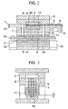
- a long lead frame 1, having portions on which the semiconductors are to be mounted, is unwound or supplied from a reel (not shown), and semiconductors 12 are bonded to the lead frame 1, and are wire-bonded to the lead frame 1.
- the lead frame 1 is guided by a feed guide 10 into a mold 4 so that a predetermined length of the lead frame 1 is set in the mold 4.
- the feed guide 10 is supported by return pins 11.
- Lower ends of the return pins 11 are supported by a support plate 18 which is moved upward and downward by a drive cylinder 16.
- the mold 4 comprises an upper mold 2 and a lower mold 3.
- the upper mold 2 can be moved upward away from the lower mold 3 by drive means (not shown) so that the mold 4 can be opened.
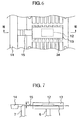
- Ejector pins 6 extend slidably through the lower mold 3 to cavities 34 in the mold 4. Lower ends of the ejector pins 6 are supported by an ejector pin operating plate 17. The plate 17 is connected to the support plate 18, and is moved upward and downward by the drive cylinder 16. Referring to Figs. 6 and 7, a molding compound from an injection molding machine is filled in each cavity 34 in the mold 4 through a runner 14 and a gate 15. Gate cut pins 7 are provided for opening and closing the respective gates 15, lower ends of which pins are supported by a pin support plate 19. The pin support plate 19 is moved upward and downward with a distance t (see Fig. 3) by drive means (not shown) so that the gate cut pins 7 can open and close the respective gates 15.
- a feed mechanism 9 for moving another feed guide 8 in a right-hand direction (Fig. 2) is provided between the lower mold 3 and the feed guide 8.
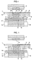
- the molding compound is injected into the cavities 34 in the mold 4, and the gate cut pins 7 are operated to shut off the gates 15, so that each molded product (comprising the semiconductor 12 encapsulated by the resin molding compound 13) is isolated from the runner 14.
- the upper mold 2 is moved upward to open the mold 4 as shown in Fig. 5.
- the drive cylinder 16 is driven to move the support plate 18 upward.
- the feed guides 10 and 8, supported by the return pins 11 are moved upward away from the lower mold 3.
- the ejector pin operating plate 17 is also moved upward, so that the ejector pins 6 eject the respective molded products from the respective cavities 34 in the lower mold 3. They are discharged from the lower mold 3.
- the feed mechanism 9 is operated to move the feed guide 8 in the right-hand direction, thereby moving a molded lead frame portion 5 by a predetermined distance in the right-hand direction.
- the drive cylinder 16 is operated to move the return pins 11 and the ejector pins 6 downward.
- the lead frame 1 is again set in the lower mold 3, and then the upper mold 2 is moved downward to close the mold 4.
- the above-mentioned molding is repeated on a non-molded portion of the lead frame 1 subsequent to the precedingly-molded lead frame portion 5.
- Figs. 6 and 7 are enlarged views showing the runner, the gate and the cavity in the mold, and show a condition immediately after the molding compound 13 is filled in the cavity 34.
- the injected molding compound is filled in the respective cavities 34 through the sprue (not shown), the runner 14 and the gate 15.
- the lead frame 1, each having the semiconductor 12 bonded thereto, have been set again in the cavities 34, respectively.
- each gate cut pin 7 is moved upward by a distance corresponding to the height t of the gate, thereby shutting off the gate 15.
- the mold is opened, and the molded products are ejected.
- the molding compound cured in the runner 14 is isolated from the molded lead frame portion 5.
- the molded lead frame portion 5 is smoothly transferred by the feed mechanism 9, so that the subsequent molding operation can be carried out.
- the hoop molding is used, and therefore the sequential molding process can be automatically effected in an unmanned manner, which process includes the steps of unwinding of the lead frame, bonding of the semiconductors, wire bonding, seeding of the lead frame in the mold, molding, removing the molded produces, separating the molded produces from the lead frame, and bending of the leads of the molded products Therefore, the sequential steps from the unwinding of the lead frame to the post-processing of the molded product can be carried out in one system.
- a further embodiment of the present invention is characterized in that a rotary molding method is used.
- a rotary injection molding apparatus 35 comprises an injection molding machine 20 having a hopper 23, and a rotary table 24 provided in generally juxtaposed relation co the injection molding machine 20.
- Four mold devices 25, 26, 27 and 28 are mounted on the rotary table 24, and are circumferentially spaced by 90° from one another.
- a nozzle 36 of the injection molding machine 20 communicates with a sprue-runner 32 (see Fig. 10) of the mold device 25, and a molding compound is filled in the mold device 25.
- the molding compound is filled in the mold device 25, and is held at a predetermined pressure, and at the same time the curing of the molding compound proceeds in the mold devices 26 and 27 where the mold is closed or clamped.
- the mold is opened to remove the molded products (each comprising a semiconductor element 31 encapsulated by the molding compound 30), and lead frames 29 are set in the mold and the mold is closed.
- gate cut pins 33 are provided in each mold, and after the molding compound is injected and filled in the mold, the gate cut pins 33 are operated to shut off the gates so as to isolate the molded products from the sprue-runner 32, thereby facilitating the removal of the molded product and the post-processing.
- the separation of the molded products from the lead frame and the bending of leads of the molded products are effected at the same time. At this time, flashes formed on the periphery of each molded product are easily removed since such burrs are usually very thin.
- the sequential steps from the setting of the lead frame in the mold to the post-processing of the molded product can be carried out in one system.
- the encapsulation of the semiconductors by the epoxy resin molding compound can be effected continuously for a long time period by the injection molding of the rotary molding type without any problem.
- the molding operation can be completely automated.
- the molding compound in the form of powder or granules can be supplied to the injection molding machine, and therefore does not need to be preformed into a tablet-like shape as in the transfer molding. Therefore, vase apparatus and time required for the tableting are omitted. Since the pre-processing such as the tableting is unnecessary, there is little possibility that impurities are included into the molding compound. Sprueless molding and sprue-runnerless molding can be adopted, and therefore the ratio of the cured material (waste) other than the molded products is greatly reduced.
Landscapes
- Engineering & Computer Science (AREA)
- Manufacturing & Machinery (AREA)
- Mechanical Engineering (AREA)
- Encapsulation Of And Coatings For Semiconductor Or Solid State Devices (AREA)
- Injection Moulding Of Plastics Or The Like (AREA)
Claims (8)
- Procédé de fabrication d'un dispositif à semi-conducteur encapsulé de résine par injection d'un composé de moulage en résine époxy dans un moule à injection, dans lequel une grille de connexion (1), à laquelle un semi-conducteur (12) a été fixé et soudé à l'aide de fils, est ajustée de manière fixe en tant que pièce rapportée dans le moule à injection (4), et par durcissement de ce composé de moulage en résine époxy dans ledit moule à injection, caractérisé par les étapes suivantes consistant à:augmenter progressivement une pression d'injection de ladite machine de moulage par injection de telle sorte qu'une pression maximale allant de 30 kg/cm2 à 300 kg/cm2 soit obtenue au moment où de 80 % à 95 % d'une quantité totale du composé de moulage en résine époxy à injecter est injecté dans le moule à injection; etinjecter le composé de moulage en résine époxy à une pression d'injection allant de 20 kg/cm2 à 100 kg/cm2.
- Procédé selon la revendication 1, dans lequel le remplissage dudit composé de moulage dans ledit moule est interrompu au moyen de portes de fermeture (15) à travers lesquelles ledit composé de moulage s'écoule dans ledit moule (4), après que ledit composé de moulage a rempli ledit moule (4) et avant que ledit moule (4) soit ouvert.
- Procédé selon la revendication 1, comprenant en outre l'étape consistant à chauffer un cylindre de ladite machine de moulage par injection à 65°C -110°C.
- Procédé selon la revendication 1, comprenant en outre les étapes consistant à:positionner une pluralité desdits éléments de semi-conducteur (12) sur ladite grille de connexion (1) en série, de manière intermittente;souder à l'aide de fils lesdits éléments de semi-conducteur (12) à ladite grille de connexion (1);définir ladite grille de connexion (1) en tant que pièce rapportée dans ledit moule (4);injecter ledit composé de moulage en résine époxy dans ledit moule (4) par ladite machine de moulage par injection;éjecter la grille de connexion moulée (1) dudit moule (4) après le durcissement dudit composé de moulage;déplacer ladite grille de connexion (1) dans une direction longitudinale sur une longueur prédéterminée, et de nouveau définir ladite grille de connexion en tant que pièce rapportée dans ledit moule; etinjecter ledit composé de moulage en résine époxy dans ledit moule (4) par rapport à une partie subséquente de ladite grille de connexion.
- Procédé selon la revendication 1, comprenant en outre les étapes consistant à:prévoir un appareil de moulage par injection rotatif (35) dans lequel une pluralité de dispositifs formant moules (25, 26, 27, 28) sont montés sur une table tournante (24), et sont espacés selon un angle prédéterminé les uns des autres;définir ladite grille de connexion, l'élément de semi-conducteur (31) étant lié à celle-ci et soudé à l'aide de fils à celle-ci, dans chacun desdits dispositifs formant moules (25, 26, 27, 28);injecter ledit composé de moulage en résine époxy dans l'un desdits dispositifs formant moules (25, 26, 27, 28) au niveau d'une position d'injection par ladite machine de moulage par injection (35);faire tourner de manière intermittente ladite table tournante (24) selon ledit angle prédéterminé afin d'amener le prochain dispositif formant moule vers ladite injection; etretirer le dispositif à semi-conducteur encapsulé de résine dudit dispositif formant moule (25, 26, 27, 28).
- Procédé selon la revendication 1, dans lequel ledit composé de moulage en résine époxy comprend une résine époxy, une résine phénolique en tant qu'agent de durcissement, un accélérateur de durcissement, et une charge inorganique.
- Procédé selon la revendication 1, dans lequel ledit moule est un moule à injection sans carotte.
- Procédé selon la revendication 1, dans lequel ledit moule est un moule sans canal.
Priority Applications (1)
| Application Number | Priority Date | Filing Date | Title |
|---|---|---|---|
| EP99123356A EP0985513B1 (fr) | 1996-01-31 | 1996-07-18 | Procédé d'encapsulation d'un dispositif semi-conducteur par une résine époxy |
Applications Claiming Priority (6)
| Application Number | Priority Date | Filing Date | Title |
|---|---|---|---|
| JP1524896 | 1996-01-31 | ||
| JP15247/96 | 1996-01-31 | ||
| JP1524796 | 1996-01-31 | ||
| JP1524896 | 1996-01-31 | ||
| JP15248/96 | 1996-01-31 | ||
| JP1524796 | 1996-01-31 |
Related Child Applications (1)
| Application Number | Title | Priority Date | Filing Date |
|---|---|---|---|
| EP99123356A Division EP0985513B1 (fr) | 1996-01-31 | 1996-07-18 | Procédé d'encapsulation d'un dispositif semi-conducteur par une résine époxy |
Publications (3)
| Publication Number | Publication Date |
|---|---|
| EP0787569A2 EP0787569A2 (fr) | 1997-08-06 |
| EP0787569A3 EP0787569A3 (fr) | 1999-04-21 |
| EP0787569B1 true EP0787569B1 (fr) | 2002-10-02 |
Family
ID=26351369
Family Applications (2)
| Application Number | Title | Priority Date | Filing Date |
|---|---|---|---|
| EP96111611A Expired - Lifetime EP0787569B1 (fr) | 1996-01-31 | 1996-07-18 | Procédé d'encapsulation d'un dispositif semi-conducteur par une résine époxy |
| EP99123356A Expired - Lifetime EP0985513B1 (fr) | 1996-01-31 | 1996-07-18 | Procédé d'encapsulation d'un dispositif semi-conducteur par une résine époxy |
Family Applications After (1)
| Application Number | Title | Priority Date | Filing Date |
|---|---|---|---|
| EP99123356A Expired - Lifetime EP0985513B1 (fr) | 1996-01-31 | 1996-07-18 | Procédé d'encapsulation d'un dispositif semi-conducteur par une résine époxy |
Country Status (7)
| Country | Link |
|---|---|
| US (1) | US5672549A (fr) |
| EP (2) | EP0787569B1 (fr) |
| KR (1) | KR100429046B1 (fr) |
| CN (1) | CN1096706C (fr) |
| DE (2) | DE69625623T2 (fr) |
| MY (1) | MY112215A (fr) |
| SG (2) | SG91806A1 (fr) |
Families Citing this family (31)
| Publication number | Priority date | Publication date | Assignee | Title |
|---|---|---|---|---|
| EP1023980B1 (fr) | 1999-01-28 | 2003-04-02 | Fujifilm Electronic Imaging Limited | Procédé de création d'une surface porteuse |
| DE19929026B4 (de) * | 1999-06-25 | 2011-02-24 | Robert Bosch Gmbh | Verfahren zur Herstellung eines Drucksensors |
| US6523254B1 (en) * | 2000-04-19 | 2003-02-25 | Micron Technology, Inc. | Method for gate blocking x-outs during a molding process |
| CN1309037C (zh) * | 2003-11-05 | 2007-04-04 | 黄伟鹏 | 一种一体化接收头的塑模制造方法及其复合塑料模粒 |
| NL1025905C2 (nl) * | 2004-04-08 | 2005-10-11 | Fico Bv | Werkwijze en inrichting voor het aan een vormholte toevoeren van omhulmateriaal. |
| SI2409707T1 (sl) | 2004-04-15 | 2015-07-31 | Alkermes Pharma Ireland Limited | Naprava s podaljšanim sproščanjem na osnovi polimerov |
| US7456254B2 (en) * | 2004-04-15 | 2008-11-25 | Alkermes, Inc. | Polymer-based sustained release device |
| US11246913B2 (en) | 2005-02-03 | 2022-02-15 | Intarcia Therapeutics, Inc. | Suspension formulation comprising an insulinotropic peptide |
| JP4890804B2 (ja) * | 2005-07-19 | 2012-03-07 | 富士通セミコンダクター株式会社 | 半導体装置及びその製造方法 |
| BRPI0709403A2 (pt) * | 2006-03-27 | 2011-07-12 | Matteo Amoruso | método para fabricar um cartão de segurança (protegido) pessoal dotado de dois processadores e cartão |
| EP2049081B1 (fr) | 2006-08-09 | 2012-11-14 | Intarcia Therapeutics, Inc. | Systemes d'administration osmotiques et ensembles pistons |
| JP4858966B2 (ja) | 2006-11-02 | 2012-01-18 | Towa株式会社 | 電子部品の圧縮成形方法及び成形装置 |
| TW200830573A (en) * | 2007-01-03 | 2008-07-16 | Harvatek Corp | Mold structure for packaging light-emitting diode chip and method for packaging light-emitting diode chip |
| HRP20130259T1 (hr) | 2007-04-23 | 2013-04-30 | Intarcia Therapeutics, Inc. | Suspenzijske formulacije inzulinotropnih peptida i njihove uporabe |
| KR100852463B1 (ko) | 2007-08-24 | 2008-08-14 | 세크론 주식회사 | 에폭시 몰딩 컴파운드 공급 방법 및 장치 |
| DK2240155T3 (da) | 2008-02-13 | 2012-09-17 | Intarcia Therapeutics Inc | Indretninger, formuleringer og fremgangsmåder til levering af flere gavnlige midler |
| SMT201700583T1 (it) | 2009-09-28 | 2018-01-11 | Intarcia Therapeutics Inc | Instaurazione e/o terminazione rapida di erogazione di farmaci in modo sostanzialmente stazionario |
| PL2987600T3 (pl) * | 2009-12-24 | 2018-07-31 | Curti Costruzioni Meccaniche S.P.A. | Wtryskarka |
| JP5456548B2 (ja) * | 2010-04-12 | 2014-04-02 | 住友重機械工業株式会社 | 樹脂成形金型及び射出成形方法 |
| US20120208755A1 (en) | 2011-02-16 | 2012-08-16 | Intarcia Therapeutics, Inc. | Compositions, Devices and Methods of Use Thereof for the Treatment of Cancers |
| KR101354781B1 (ko) * | 2012-06-11 | 2014-01-23 | 앰코 테크놀로지 코리아 주식회사 | 반도체 디바이스의 제조 방법 |
| US9889085B1 (en) | 2014-09-30 | 2018-02-13 | Intarcia Therapeutics, Inc. | Therapeutic methods for the treatment of diabetes and related conditions for patients with high baseline HbA1c |
| CN104387601B (zh) | 2014-11-06 | 2017-02-08 | 东莞市德聚胶接技术有限公司 | 一种uv环氧树脂滴注成型方法及应用 |
| US10925639B2 (en) | 2015-06-03 | 2021-02-23 | Intarcia Therapeutics, Inc. | Implant placement and removal systems |
| RU2760007C2 (ru) | 2016-05-16 | 2021-11-22 | Интарсия Терапьютикс, Инк. | Полипептиды, селективные к рецепторам глюкагона, и способы их применения |
| USD860451S1 (en) | 2016-06-02 | 2019-09-17 | Intarcia Therapeutics, Inc. | Implant removal tool |
| USD840030S1 (en) | 2016-06-02 | 2019-02-05 | Intarcia Therapeutics, Inc. | Implant placement guide |
| CN110225762A (zh) | 2017-01-03 | 2019-09-10 | 因塔西亚制药公司 | 包括glp-1受体激动剂的连续施用和药物的共同施用的方法 |
| USD933219S1 (en) | 2018-07-13 | 2021-10-12 | Intarcia Therapeutics, Inc. | Implant removal tool and assembly |
| KR102153725B1 (ko) * | 2018-12-12 | 2020-09-09 | 주식회사 디에스시동탄 | 시트프레임 어셈블리 및 그 제조방법 |
| CN114589852B (zh) * | 2022-03-17 | 2024-11-29 | 黄高维 | 一种工业生产用树脂井盖上料装置 |
Family Cites Families (26)
| Publication number | Priority date | Publication date | Assignee | Title |
|---|---|---|---|---|
| US1604545A (en) | 1925-03-14 | 1926-10-26 | Bragg Kliesrath Corp | Hydraulic brake mechanism for automotive vehicles |
| JPS597008A (ja) * | 1982-07-03 | 1984-01-14 | Toshiba Corp | 高密度タブレツトおよびそれを使用した半導体樹脂封止方法 |
| NL8302530A (nl) * | 1983-07-14 | 1985-02-01 | Jacob Van Noort | Integrated circuit en werkwijze, spuitgietvorm en spuitgietmachine ter vervaardiging van voorwerpen. |
| JPS60119734A (ja) * | 1983-12-01 | 1985-06-27 | Japan Steel Works Ltd:The | 電子部品の樹脂封止方法 |
| WO1985004418A1 (fr) | 1984-03-27 | 1985-10-10 | Transgene S.A. | Vecteurs d'expression de l'hirudine, cellules transformees et procede de preparation de l'hirudine |
| DE3438296A1 (de) | 1984-04-18 | 1985-11-07 | Hoechst Ag, 6230 Frankfurt | Neue polypeptide mit blutgerinnungshemmender wirkung, verfahren zu deren herstellung bzw. gewinnung, deren verwendung und diese enthaltende mittel |
| ATE64956T1 (de) | 1984-06-14 | 1991-07-15 | Ciba Geigy Ag | Verfahren zur herstellung von thrombininhibitoren. |
| DE3445517C2 (de) | 1984-12-13 | 1993-11-18 | Ciba Geigy | Für ein Hirudin-ähnliches Protein codierende DNA-Sequenz und Verfahren zur Herstellung eines Hirudin-ähnlichen Proteins |
| DE3506992A1 (de) | 1985-02-27 | 1986-08-28 | Plantorgan Werk Heinrich G.E. Christensen, KG, 2903 Bad Zwischenahn | Modifizierte hirudine, verfahren zu deren herstellung und pharmazeutische mittel, die diese wirkstoffe enthalten |
| ES2055149T3 (es) | 1985-04-11 | 1994-08-16 | Hoechst Ag | Derivado de hirudina. |
| FR2593518B1 (fr) | 1985-05-02 | 1989-09-08 | Transgene Sa | Vecteurs d'expression et de secretion de l'hirudine par les levures transformees |
| DE3689525D1 (de) | 1985-07-17 | 1994-02-24 | Hoechst Ag | Neue Polypeptide mit blutgerinnungshemmender Wirkung, Verfahren zu deren Herstellung bzw. Gewinnung, deren Verwendung und diese enthaltende Mittel. |
| US5179039A (en) * | 1988-02-05 | 1993-01-12 | Citizen Watch Co., Ltd. | Method of making a resin encapsulated pin grid array with integral heatsink |
| AU614121B2 (en) | 1988-05-04 | 1991-08-22 | Novartis Ag | Improvements in the production of polypeptides |
| DE3819686A1 (de) * | 1988-06-09 | 1989-12-14 | Siemens Ag | Verfahren zum umspritzen von elektrischen bauelementen mit duroplastischen kunststoffen |
| JPH0289613A (ja) * | 1988-09-27 | 1990-03-29 | Somar Corp | エポキシ樹脂組成物の射出成形方法及びそれに用いる組成物 |
| FR2645175B1 (fr) | 1989-03-31 | 1994-02-18 | Transgene Sa | Souche de saccharomyces cerevisiaeproductrice d'une proteine heterologue et procede de preparation de ladite proteine heterologue par fermentation de ladite souche |
| JPH02306639A (ja) * | 1989-05-22 | 1990-12-20 | Toshiba Corp | 半導体装置の樹脂封入方法 |
| US5367766A (en) * | 1990-08-01 | 1994-11-29 | Staktek Corporation | Ultra high density integrated circuit packages method |
| TW208759B (fr) * | 1991-10-24 | 1993-07-01 | American Telephone & Telegraph | |
| JPH06124971A (ja) * | 1992-10-14 | 1994-05-06 | Nec Corp | 樹脂封止金型 |
| US5525547A (en) * | 1992-12-16 | 1996-06-11 | Hitachi, Ltd. | Method of fabricating a molded semiconductor device having blocking banks between leads |
| JP2927660B2 (ja) * | 1993-01-25 | 1999-07-28 | シャープ株式会社 | 樹脂封止型半導体装置の製造方法 |
| US5474958A (en) * | 1993-05-04 | 1995-12-12 | Motorola, Inc. | Method for making semiconductor device having no die supporting surface |
| JPH07137083A (ja) * | 1993-11-18 | 1995-05-30 | Sumitomo Jukikai Plast Mach Kk | 射出成形装置 |
| JPH0867745A (ja) * | 1994-08-30 | 1996-03-12 | Sumitomo Bakelite Co Ltd | エポキシ樹脂組成物 |
-
1996
- 1996-07-18 DE DE69625623T patent/DE69625623T2/de not_active Expired - Fee Related
- 1996-07-18 EP EP96111611A patent/EP0787569B1/fr not_active Expired - Lifetime
- 1996-07-18 EP EP99123356A patent/EP0985513B1/fr not_active Expired - Lifetime
- 1996-07-18 DE DE69624087T patent/DE69624087T2/de not_active Expired - Fee Related
- 1996-07-19 MY MYPI96002974A patent/MY112215A/en unknown
- 1996-07-22 US US08/681,348 patent/US5672549A/en not_active Expired - Lifetime
- 1996-07-22 SG SG9803602A patent/SG91806A1/en unknown
- 1996-07-22 SG SG1996010299A patent/SG48465A1/en unknown
- 1996-07-26 CN CN96110843A patent/CN1096706C/zh not_active Expired - Fee Related
- 1996-07-26 KR KR1019960030722A patent/KR100429046B1/ko not_active Expired - Fee Related
Also Published As
| Publication number | Publication date |
|---|---|
| KR970060461A (ko) | 1997-08-12 |
| CN1156329A (zh) | 1997-08-06 |
| KR100429046B1 (ko) | 2004-09-18 |
| EP0985513B1 (fr) | 2003-01-02 |
| US5672549A (en) | 1997-09-30 |
| EP0985513A3 (fr) | 2000-03-22 |
| EP0787569A2 (fr) | 1997-08-06 |
| DE69625623D1 (de) | 2003-02-06 |
| CN1096706C (zh) | 2002-12-18 |
| DE69625623T2 (de) | 2003-11-06 |
| SG48465A1 (en) | 1998-04-17 |
| EP0787569A3 (fr) | 1999-04-21 |
| MY112215A (en) | 2001-04-30 |
| DE69624087D1 (de) | 2002-11-07 |
| SG91806A1 (en) | 2002-10-15 |
| EP0985513A2 (fr) | 2000-03-15 |
| DE69624087T2 (de) | 2003-06-05 |
Similar Documents
| Publication | Publication Date | Title |
|---|---|---|
| EP0787569B1 (fr) | Procédé d'encapsulation d'un dispositif semi-conducteur par une résine époxy | |
| JP2970569B2 (ja) | 樹脂封止方法および樹脂封止金型装置 | |
| JP2778608B2 (ja) | 樹脂モールド型半導体装置の製造方法 | |
| US5254501A (en) | Same-side gated process for encapsulating semiconductor devices | |
| GB2253182A (en) | Transfer moulding device for encapsulating electronic components | |
| US20130140737A1 (en) | Stacked substrate molding | |
| JP2004235530A (ja) | 封止成形装置及びそれを用いた封止成形体の製造方法 | |
| JP2567603B2 (ja) | 連続自動樹脂封止方法 | |
| JP3357141B2 (ja) | 樹脂モールド装置 | |
| JP2666630B2 (ja) | 半導体装置の製造方法 | |
| US5169586A (en) | Method of manufacturing resin-sealed type semiconductor device | |
| JP3195840B2 (ja) | 樹脂モールド装置及びその制御方法 | |
| JP3192957B2 (ja) | 半導体封止方法 | |
| JPS6146051B2 (fr) | ||
| JPS6154633A (ja) | 半導体樹脂封止用金型 | |
| JP3543742B2 (ja) | 樹脂封止成形装置 | |
| JPH10138280A (ja) | 半導体封止方法 | |
| JPH08264575A (ja) | 半導体封止方法 | |
| JP3147334B2 (ja) | 半導体装置の製造方法 | |
| JP3007851B2 (ja) | 樹脂成形方法及び樹脂成形装置 | |
| TW311270B (fr) | ||
| CN116945494A (zh) | 一种芯片塑封装置用塑封料装填结构 | |
| JPH10144711A (ja) | 半導体封止方法 | |
| JPH0737919A (ja) | 半導体素子の樹脂封止装置 | |
| JP2001196402A (ja) | 半導体装置の製造方法 |
Legal Events
| Date | Code | Title | Description |
|---|---|---|---|
| PUAI | Public reference made under article 153(3) epc to a published international application that has entered the european phase |
Free format text: ORIGINAL CODE: 0009012 |
|
| AK | Designated contracting states |
Kind code of ref document: A2 Designated state(s): DE GB IT NL |
|
| PUAL | Search report despatched |
Free format text: ORIGINAL CODE: 0009013 |
|
| AK | Designated contracting states |
Kind code of ref document: A3 Designated state(s): DE GB IT NL |
|
| 17P | Request for examination filed |
Effective date: 19990607 |
|
| 17Q | First examination report despatched |
Effective date: 19990729 |
|
| GRAG | Despatch of communication of intention to grant |
Free format text: ORIGINAL CODE: EPIDOS AGRA |
|
| GRAG | Despatch of communication of intention to grant |
Free format text: ORIGINAL CODE: EPIDOS AGRA |
|
| GRAH | Despatch of communication of intention to grant a patent |
Free format text: ORIGINAL CODE: EPIDOS IGRA |
|
| GRAH | Despatch of communication of intention to grant a patent |
Free format text: ORIGINAL CODE: EPIDOS IGRA |
|
| GRAA | (expected) grant |
Free format text: ORIGINAL CODE: 0009210 |
|
| AK | Designated contracting states |
Kind code of ref document: B1 Designated state(s): DE GB IT NL |
|
| PG25 | Lapsed in a contracting state [announced via postgrant information from national office to epo] |
Ref country code: NL Free format text: LAPSE BECAUSE OF FAILURE TO SUBMIT A TRANSLATION OF THE DESCRIPTION OR TO PAY THE FEE WITHIN THE PRESCRIBED TIME-LIMIT Effective date: 20021002 Ref country code: IT Free format text: LAPSE BECAUSE OF FAILURE TO SUBMIT A TRANSLATION OF THE DESCRIPTION OR TO PAY THE FEE WITHIN THE PRE;WARNING: LAPSES OF ITALIAN PATENTS WITH EFFECTIVE DATE BEFORE 2007 MAY HAVE OCCURRED AT ANY TIME BEFORE 2007. THE CORRECT EFFECTIVE DATE MAY BE DIFFERENT FROM THE ONE RECORDED.SCRIBED TIME-LIMIT Effective date: 20021002 |
|
| REG | Reference to a national code |
Ref country code: GB Ref legal event code: FG4D |
|
| REF | Corresponds to: |
Ref document number: 69624087 Country of ref document: DE Date of ref document: 20021107 |
|
| NLV1 | Nl: lapsed or annulled due to failure to fulfill the requirements of art. 29p and 29m of the patents act | ||
| PG25 | Lapsed in a contracting state [announced via postgrant information from national office to epo] |
Ref country code: GB Free format text: LAPSE BECAUSE OF NON-PAYMENT OF DUE FEES Effective date: 20030718 |
|
| PLBE | No opposition filed within time limit |
Free format text: ORIGINAL CODE: 0009261 |
|
| STAA | Information on the status of an ep patent application or granted ep patent |
Free format text: STATUS: NO OPPOSITION FILED WITHIN TIME LIMIT |
|
| 26N | No opposition filed |
Effective date: 20030703 |
|
| GBPC | Gb: european patent ceased through non-payment of renewal fee |
Effective date: 20030718 |
|
| PGFP | Annual fee paid to national office [announced via postgrant information from national office to epo] |
Ref country code: DE Payment date: 20090716 Year of fee payment: 14 |
|
| PG25 | Lapsed in a contracting state [announced via postgrant information from national office to epo] |
Ref country code: DE Free format text: LAPSE BECAUSE OF NON-PAYMENT OF DUE FEES Effective date: 20110201 |
|
| REG | Reference to a national code |
Ref country code: DE Ref legal event code: R119 Ref document number: 69624087 Country of ref document: DE Effective date: 20110201 |