EP0788013A2 - Substrat d'électrodes pour dispositif à cristal liquide et son procédé de fabrication - Google Patents
Substrat d'électrodes pour dispositif à cristal liquide et son procédé de fabrication Download PDFInfo
- Publication number
- EP0788013A2 EP0788013A2 EP97300593A EP97300593A EP0788013A2 EP 0788013 A2 EP0788013 A2 EP 0788013A2 EP 97300593 A EP97300593 A EP 97300593A EP 97300593 A EP97300593 A EP 97300593A EP 0788013 A2 EP0788013 A2 EP 0788013A2
- Authority
- EP
- European Patent Office
- Prior art keywords
- electrodes
- resin
- liquid crystal
- spacing
- curing
- Prior art date
- Legal status (The legal status is an assumption and is not a legal conclusion. Google has not performed a legal analysis and makes no representation as to the accuracy of the status listed.)
- Granted
Links
Images


Classifications
-
- G—PHYSICS
- G02—OPTICS
- G02F—OPTICAL DEVICES OR ARRANGEMENTS FOR THE CONTROL OF LIGHT BY MODIFICATION OF THE OPTICAL PROPERTIES OF THE MEDIA OF THE ELEMENTS INVOLVED THEREIN; NON-LINEAR OPTICS; FREQUENCY-CHANGING OF LIGHT; OPTICAL LOGIC ELEMENTS; OPTICAL ANALOGUE/DIGITAL CONVERTERS
- G02F1/00—Devices or arrangements for the control of the intensity, colour, phase, polarisation or direction of light arriving from an independent light source, e.g. switching, gating or modulating; Non-linear optics
- G02F1/01—Devices or arrangements for the control of the intensity, colour, phase, polarisation or direction of light arriving from an independent light source, e.g. switching, gating or modulating; Non-linear optics for the control of the intensity, phase, polarisation or colour
- G02F1/13—Devices or arrangements for the control of the intensity, colour, phase, polarisation or direction of light arriving from an independent light source, e.g. switching, gating or modulating; Non-linear optics for the control of the intensity, phase, polarisation or colour based on liquid crystals, e.g. single liquid crystal display cells
- G02F1/133—Constructional arrangements; Operation of liquid crystal cells; Circuit arrangements
- G02F1/1333—Constructional arrangements; Manufacturing methods
- G02F1/1343—Electrodes
- G02F1/13439—Electrodes characterised by their electrical, optical, physical properties; materials therefor; method of making
Definitions
- the present invention relates to an electrode substrate including at least two types of electrodes and a process for producing the electrode substrate.
- the present invention also relates to a liquid crystal device using the electrode substrates and a process for producing the liquid crystal device.
- Figure 1A shows an embodiment of a structure of such a liquid crystal panel.
- a liquid crystal panel P1 includes a pair of electrode substrates 1 applied to each other with a sealing agent 2 so as to leave a spacing therebetween, and a liquid crystal 3 filling the spacing.
- the liquid crystal 3 comprises a ferroelectric liquid crystal, thus constituting a ferroelectric liquid crystal panel.
- Each of the electrode plates 1 is provided with a glass substrate 5 the surface of which is provided with a plurality of transparent electrodes 6 of indium-tin oxide (ITO).
- the transparent electrodes 6 generally have a thickness of 50 - 150 nm and are formed into a stripe pattern by patterning treatment as shown in Figure 1B.
- a ca. 500 - 3000 ⁇ -thick insulating film 7 comprising, e.g., silicon oxide or titanium oxide for preventing an occurrence of short-circuit is formed, and further thereon, an alignment control film 9 comprising, e.g., polyimide is formed.
- the ferroelectric liquid crystal 3 generally comprises a chiral smectic liquid crystal assuming, e.g., chiral smectic C (SmC*) phase or chiral smectic H (SmH*) phase.
- the ferroelectric liquid crystal 3 shows a helical alignment (orientation) wherein liquid crystal molecules are twisted in their (average) long axis direction in case where the influence of the pair of electrode substrates 1 thereon is small (e.g., the case of too distant electrode plates 1 with a spacing therebetween of above 100 ⁇ m) but the helical alignment of the ferroelectric liquid crystal 3 in the long axis direction is suppressed (or unwounded) by providing the liquid crystal panel P1 with a small cell thickness of, e.g., 1 - 3 ⁇ m, as described by N.A. Clark et al. "MCLC", vol. 94, pp. 213 - 234 (1983).
- the liquid crystal panel P1 is driven by applying a voltage to oppositely disposed transparent electrodes 6 and accordingly the liquid crystal 3 disposed between the oppositely disposed transparent electrodes 6 constitutes a capacitive load in an electric circuit.
- the transparent electrodes 6 has a sheet resistance of 20 - 400 ohm and a volume resistivity of 200x10 -8 - 4000x10 -8 ohm.m, thus being liable to cause propagation delay of a voltage waveform therein.
- it has been difficult to provide a resultant liquid crystal panel with a high resolution and a large picture area. This problem has been more noticeable in the case of the ferroelectric liquid crystal panel having a small liquid crystal layer thickness of 1- 2 ⁇ m when compared with a twisted nematic (TN)-type liquid crystal device.
- TN twisted nematic
- a method providing a larger thickness to the transparent electrode 6 may be adopted but is accompanied with a longer film formation time and a lowering in adhesiveness to the glass substrate 1.
- a resultant liquid crystal panel shows a lower transmittance and therefore the transparent electrodes 6 per se are visually recognized, thus deteriorating display qualities of the liquid crystal panel.
- the metal electrodes cannot be made thick due to the following factors (i) and (ii), thus resulting in a limit to improvement in propagation delay of a voltage waveform.
- Figures 2A and 2B are schematic views of an embodiment of a structure of a liquid crystal panel employing such a method.
- a liquid crystal panel P2 includes a pair of substantially oppositely disposed electrode substrates 10 each provided with a transparent or transmissive substrate (glass substrate) 11 on which a plurality of ca. 1 ⁇ m-thick metal electrodes (first electrodes) 12 in a stripe shape are disposed with a certain spacing. As specifically shown in Figure 2B, the spacing is filled with a ultraviolet light-curable resin (hereinafter referred to as "UV curing resin") 13S.
- UV curing resin ultraviolet light-curable resin
- the reference numeral 13S is used for describing a UV curing resin in a solid state after curing
- a reference numeral 13L is used for describing it in a liquid state before curing
- a reference numeral 13 is used for describing the UV curing resin in case where a state thereof need not be particularly differentiated.
- the UV curing resin 13S (13 in Figure 2A) and the metal electrodes 12 together constitute one surface on which a plurality of transparent electrodes (second electrodes) 6 in a stripe shape are formed and further thereon, an insulating film 7 and an alignment control film 9 are successively formed to prepare an electrode substrate 10.
- the transparent electrodes 6 are disposed along the metal electrodes 12 so that they are in contact with associated metal electrodes, respectively.
- a pair of the electrode substrates 10 are applied to each other with a sealing agent 2 so as to leave a gap filled with a liquid crystal 3 as described above to prepare a liquid crystal panel P2.
- a thick metal layer 14 is formed on the surface of a glass substrate 11 by, e.g., a sputtering process (Figure 3A).
- the metal layer 14 is subjected to patterning through a photolithographic process to form a multiplicity of stripe-shaped metal electrodes (first electrodes) 12 to constitute a wiring substrate 15 having a wiring face 15a where the metal electrodes 12 are disposed ( Figure 3B).
- the wiring face 15a of the wiring substrate 15 is subjected to a surface treatment with a silane coupling agent to ensure an adhesiveness between the glass substrate 11 and a UV curing resin 13 applied onto the glass substrate 11 in a subsequent step.
- a UV curing resin 13L (before curing) is added dropwise to a smooth surface of a mold glass (smooth plate member) 16.
- the wiring face 15a of the wiring substrate 15 is superposed on the surface (supplied with the UV curable resin 13L) of the mold glass 16 so as to sandwich therebetween the UV curing resin 13L to provide a pressure-receiving member (a member subjected to pressure application) 17 ( Figure 3C).
- the UV curing resin 13L is filled in a spacing between the metal electrodes 12 at the wiring face 15a of the wiring substrate 15.
- the pressure-receiving member 17 is pressed by a pressing machine (not shown).
- a pressing machine not shown
- the surface of the metal electrodes 12 and the UV curing resin 13L supplied to the spacing between the metal electrodes 12 are caused to come in contact with the smooth surface of the mold glass 16, so that the UV curing resin 13L (in a liquid state) and the metal electrodes having the spacing filled with the UV curing resin 13L together form a smooth surface.
- the UV curing resin 13L is exposed to a ultraviolet (UV) light (or rays) L from the glass substrate 1 side by UV light irradiation providing a light energy h ⁇ , thus curing the UV curing resin 13L ( Figure 3D).
- UV ultraviolet
- a multiplicity of transparent electrodes (second electrodes) 6 are formed on the surface of the metal electrodes 12 so that respective transparent electrodes 6 are caused to come in contact with associated metal electrodes 12, respectively ( Figure 3F).
- an insulating film 7 (not shown) and an alignment control film 9 (not shown) are successively formed to provide an electrode substrate 10.
- a pair of such electrode substrates 10 are applied to each other with a sealing agent 2 to form a blank cell having a certain cell gap, which is then filled with a liquid crystal 3 to prepare a liquid crystal panel P2.
- the surface treatment with a silane coupling agent for enhancing an adhesiveness of the glass substrate 11 to the UV curable resin 13 is effected to the surface of the glass substrate 11 but is not effected to the surface of the mold glass 16 in view of peeling thereof, whereby an adhesiveness between the UV curing resin 13L and the mold glass 16 becomes smaller than an adhesiveness between the UV curing resin 13L and the glass substrate 11 but still leaves somewhat an adhesive power.
- the UV curing resin 13L generally has a shrink property at the time of curing by UV light irradiation.
- the UV curing resin 13 is partially peeled from the surface of the mold glass 16 due to the shrink property (i.e., a local adhesion of the UV curing resin 13 to the mold glass 16 is caused), so that the shrinkage of the UV curing resin 13 is partially promoted because there is no constraint thereon at the peeled portion, thus resulting in a sinkage 19 showing a remarkable unevenness in a ripple (wave) or wrinkle shape when viewed from the direction perpendicular to the metal electrode extension direction (hereinafter, referred to as "ripple-shaped sinkage") due to such a shrinkage.
- the shrink property i.e., a local adhesion of the UV curing resin 13 to the mold glass 16 is caused
- Figures 4A - 4C are schematic views for illustrating a sinkage phenomenon (an occurrence of a ripple-shaped sinkage 19).
- the metal electrodes 12 and the UV curing resin 13L filling the spacing between the metal electrodes 12 are sandwiched between the glass substrate 11 and the mold glass 16, followed by application of a pressure F (as shown in Figure 4B) to show a state before curing the UV curing resin 13L.
- the UV curing resin 13L is exposed to UV light L under no pressure application, thus changing in a shrinkage state 13S after curing of the UV curing resin 13L ( Figure 4B).
- the shrunken UV curing resin 13S consequently has a ripple-shaped sinkage after the mold glass is removed by peeling operation (Figure 4C).
- the liquid crystal panel is produced by using such a pair of electrode substrates 10, not only the surface of the transparent electrode 6 but also the surface of the alignment control film 9 are roughened or become uneven at least in an effective optical modulation region (e.g., a display region of a display device), thus resulting in an ununiform alignment state of the liquid crystal 3 or causing a local cell gap decrease leading to an electric field concentration thereat.
- an effective optical modulation region e.g., a display region of a display device
- the liquid crystal panel is accompanied with problems of occurrences of an optical state, crosstalk and an irregularity in drive characteristics, thus resulting in a lowering in image qualities.
- the metal electrodes 12 as described above per se have a permissible unevenness (with respect to adjacent resin portions) of about at most 250 nm.
- a permissible unevenness with respect to adjacent resin portions
- even the liquid crystal panel having an unevenness of at most 250 nm is accompanied with the above-mentioned problems because the effective optical modulation region which is not light-interrupted is directly adversely affected by such an unevenness although the metal electrode portion is light-interrupted.
- An object of the present invention is to provide an electrode substrate free from a ripple-shaped sinkage of a UV curing resin and having a substantially smooth surface with respect to second electrodes in at least an effective optical modulation region and a process for producing the electrode substrate.
- Another object of the present invention is to provide an electrode substrate capable of suppressing an irregularity in optical state and an occurrence of crosstalk when used in a liquid crystal device, and a process for producing the electrode substrate.
- Another object of the present invention is to provide an electrode substrate capable of preventing a propagation delay of a voltage waveform by providing a good contact state between first electrodes and second electrodes when used in a liquid crystal device, and a process for producing the electrode substrate.
- Another object of the present invention is to provide a liquid crystal device capable of being applicable to a device of a large picture area and a high resolution and a process for producing the liquid crystal device.
- a further object of the present invention is to provide a liquid crystal device excellent in display qualities and a process for producing the liquid crystal device.
- an electrode substrate comprising: a light-transmissive substrate, a plurality of first electrodes disposed with a spacing therebetween on the light-transmissive substrate, a resin filling the spacing, and a plurality of second electrodes disposed so as to be in contact with the associated first electrodes, respectively, wherein the first electrodes have a thickness h (nm) and an average surface roughness d (nm) and the resin has a curing shrinkage ratio ⁇ (%), said thickness h, average surface roughness d and curing shrinkage ratio ⁇ satisfying the following relationship: d ⁇ ⁇ h/1000.
- the first electrodes may preferably be metal electrodes and the second electrodes may preferably be transparent electrodes, particularly ITO (indium-tin oxide) electrodes.
- the first and second electrodes may preferably be supplied with an identical signal. Further, the spacing between the first electrodes may preferably be provided with a color filter layer in addition to the resin.
- the resin in the curing step of the resin, may preferably be cured after the first electrodes and the resin is subjected to pressure application with a smooth plate member.
- the curing step of the resin may preferably be performed by irradiating a ultraviolet (UV) curable resin with ultraviolet light.
- the process may preferably further comprises a step of forming a color filter layer at the spacing between the step of forming the first electrodes and the step of filling the resin.
- the step of forming the first electrodes may preferably be performed through a sputtering process while controlling a temperature of the transmissive substrate so as to provide the first electrodes with an average surface roughness d satisfying the above relationship.
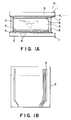
- Figure 1A is a schematic sectional view of an embodiment of a structure of a conventional liquid crystal panel and Figure 1B is a plan view for illustrating a shape of transparent electrodes used in the liquid crystal panel shown in Figure 1A.
- Figure 2A is a schematic sectional view of another embodiment of a structure of a conventional liquid crystal panel and Figure 2B is a partially enlarged sectional view of the liquid crystal panel of Figure 2A.
- Figures 3A - 3F are schematic sectional views for illustrating a conventional process for producing an electrode substrate.
- Figures 4A - 4C are schematic sectional views for illustrating a ripple-shaped sinkage of a UV curable resin occurring in a conventional electrode substrate.
- Figure 5A is a schematic sectional view of an embodiment of a structure of a liquid crystal panel according to the present invention using an electrode substrate and Figure 5B is a partially enlarged view of the electrode substrate shown in Figure 5A.
- Figures 6A - 6F are schematic sectional views for illustrating a process for producing an electrode plate according to the present invention.
- Figure 7 is a schematic sectional view of another embodiment of a structure of an electrode substrate according to the present invention.
- Figure 5A is a schematic sectional view showing a cell structure of a liquid crystal panel P3 according to the present invention.
- the liquid crystal panel P3 includes a pair of substantially oppositely disposed electrode substrates 20 each provided with a transparent or transmissive substrate (glass substrate) 11 on which a plurality of metal electrodes (first electrodes) 22 in a stripe shape are disposed with a certain spacing. As specifically shown in Figure 5B, the spacing is filled with a ultraviolet light-curable (curing) resin 13S.
- the transparent electrodes 6 are disposed along the metal electrodes 22 so that they are in contact with associated metal electrodes, respectively.
- a pair of the electrode substrates 20 are applied to each other with a sealing agent 2 so as to leave a gap to be filled with a liquid crystal 3 as described above to prepare a liquid crystal panel P3.
- the transparent electrodes comprised an ITO film and the glass substrate 11 had a size of 300x340 mm.
- UV curing resin 13 an acrylic monomer-based UV curable resin having a curing shrinkage ratio ⁇ of 10 % (manufactured by Nippon Kayaku K.K.) was used.
- the known UV curing resins generally exhibit a curing shrinkage ratio ⁇ of 6 - 10 % (for acrylic monomer-type) and of 2 - 5 % (for epoxy resin-type).
- the average surface roughness d may preferably be at most 200 nm in view of uniform cell gap.
- the sputtering conditions were as follows.
- the average surface roughness d is determined based on values measured by using a surface roughness meter ("Alpha-Step 500", manufactured by TENCOR INSTRUMENTS Co.) in the following manner.
- a sample metal layer (Al layer in this embodiment) is subjected to measurement of height (or depth) by using the above surface roughness meter to determine a difference in height between the highest portion and the lowest portion of the sample metal layer, thus obtaining a surface roughness.
- the measurement is performed with respect to other 8 regions, thus obtaining 9 surface roughnesses in total.
- An average surface roughness is determined as an average value of the 9 surface roughnesses measured above.
- a 50 %-solution of an adhesiveness-reinforcing agent (silane coupling agent) ("A-174", mfd. by Nippon Unicar Company Ltd.) (not shown) in isopropyl alcohol was added dropwise onto the wiring face 25a by using a spin coating while rotating the wiring substrate 25 at 2000 rpm, followed by hot curing at 100 °C.
- silane coupling agent silane coupling agent
- the UV curing resin 13L was filled in a spacing between the metal electrodes 22 and had a thickness identical to a thickness h of the metal electrodes 22.
- the pressure-receiving member 27 was then pressed by a pressing machine (not shown) with a force F, whereby a certain pressure was exerted on the surfaces of the metal electrodes 22 and the supplied UV curing resin 13L via the smooth mold glass 16.
- a certain pressure was exerted on the surfaces of the metal electrodes 22 and the supplied UV curing resin 13L via the smooth mold glass 16.
- an excessive portion of the UV curing resin 13L was removed from at least projection portions (contact portions) of the surfaces of the metal electrodes 22.
- the UV curing resin 13L was irradiated with a UV light L to effect curing thereof while causing shrinkage thereof under no pressure application ( Figure 6D).
- the above pressure applicatino may be effected at the time of UV light irradiation and the curing thereof.
- a multiplicity (plurality) of transparent electrodes (second electrodes) 6 were formed on the surface of the metal electrodes 22 so that respective transparent electrodes 6 were caused to come in contact with associated metal electrodes 22, respectively ( Figure 6F).
- an insulating film 7 (not shown) and an alignment control film 9 (not shown) were successively formed to provide an electrode substrate 20 (Figure 6E).
- a pair of such electrode substrates 20 were applied to each other with a sealing agent 2 to form a blank cell having a certain cell gap, which was then filled with a liquid crystal 3 to prepare a liquid crystal panel P3.
- the UV curing resin 13 to be cured and shrunken was not partially peeled from the mold glass 16 and was uniformly sunk by curing to suppress an occurrence of a ripple-shaped sinkage, so that the resultant (cured) UV curing resin 13S providing an effective optical modulation region was allowed to have a substantially smooth (flat) surface and the upper layers formed thereon (e.g., the transparent electrodes 6 and the alignment control layer 9) also had a substantially smooth surface, respectively.
- the resultant liquid crystal panel P3 provides advantageous effects including a uniform alignment state of the liquid crystal 3; freedom from an uneven optical state, an occurrence of crosstalk and an irregularity in drive characteristics; and good image qualities, in the effective optical modulation region.
- the metal electrodes 22 have the surface roughness d of 20 nm, so that at least a projection portion of the metal electrode surface is not covered with the UV curing resin 13L even when the resin 13L is not completely removed from the surface portion of the metal electrodes 22 by pressure application with the mold glass 16.
- a contact state of the metal electrodes 22 with the associated transparent electrodes 6 is uniformly ensured over the entire surface of the electrode substrate 20 by the projection portion, thus allowing a lowering in resistance of the transparent electrodes 6 and the associated metal electrodes 22.
- a resistance per length of 60 mm of the transparent electrodes 6 and the associated metal electrodes was measured, a uniform and low resistance of 50 ohm was attained over the entire region of the electrode substrate 20.
- the transparent electrodes 6 it is not necessary to provide the transparent electrodes 6 with a large thickness in order to remedy the problem of the voltage waveform propagation delay, so that the resultant liquid crystal panel P3 is improved in display quality because the transparent electrodes 6 are not lowered in transmittance, thus being not visually recognized.
- a film forming time of the transparent electrodes 6 is shortened and an adhesiveness of the transparent electrodes 6 to, e.g., the metal electrodes 22 is also ensured.
- the metal electrodes 22 are formed under the transparent electrodes 6 (i.e., formed on the glass substrate side, not on the liquid crystal side) in contrast with those of the conventional liquid crystal panels and provide a substantially smooth face together with the UV curing resin 13 although the unevenness resulting from the surface roughness d of the metal electrodes 22 and shrinkage of the UV curing resin 13.
- the resultant alignment control film 9 has little surface unevenness.
- Such thick metal electrodes 22 are further effective in suppressing an occurrence of the propagation delay of a voltage waveform, and the substantially smooth surface of the alignment control film 9 is effective in preventing occurrences of the difference in optical state and crosstalk as in the case of the conventional liquid crystal panels and also effective in allowing uniform rubbing to provide a uniform alignment state of liquid crystal molecules.
- a liquid crystal panel including a color filter layer comprising color filter segments of red (R), green (G) and blue (B) was prepared in the same manner as in First Embodiment except that a color filter-forming step was effected between a first electrode-forming step and a resin-supplying step.
- Figure 7 shows a schematic sectional view of an electrode substrate 30 used for the above liquid crystal panel.
- the electrode substrate 30 has a similar structure as in that of Figure Embodiment except for closely disposing a color filter layer 31 comprising color filter segments of R, G and B between a glass substrate 11 and a UV curing resin 13 and so as to fill a spacing between a plurality of metal electrodes 22.
- Other structural members, such as a plurality of transparent electrodes 6, an insulating film (not shown) and in alignment control film (not shown) are identical to those used in First Embodiment.
- the electrode substrate 30 was produced through the steps of a first electrode-forming step, a color-filter forming step, a resin-supplying step, a resin-curing step, a peeling step, a second electrode-forming step and other steps, respectively, in a similar manner as in First Embodiment except for the color filter-forming step.
- a solution (dispersion) of a pigment (pigment particles) in a photosensitive resin was applied onto the surface of the glass substrate (i.e., at a spacing between the metal electrodes 22) by using a roll coater, followed by selective exposure to light for development and a subsequent etching to form the color filter layer 31. Further, in the resin-supply step, a recess portion formed by the metal electrodes 22 and the color filter layer 31 was filled with a UV curing resin 13L.
- liquid crystal panel prepared in this embodiment is excellent in color display qualities.
- the sputtering process is used a a method for forming a metal layer having a prescribed average surface roughness.
- other processes including those using resistance heating and electron beam may also be adopted.
- the sputtering process may be performed by appropriately setting a sputtering temperature of 80 - 300 °C, preferably 100 - 250 °C (140 °C in the above two embodiments), in view of a desired surface roughness of resultant metal electrodes.
- the metal layer for forming a plurality of metal electrodes may have a multi-layer structure consisting of at least two layers wherein a top layer is selectively subjected to etching.
- the observation was performed with respect to the entire effective optical modulation region by using a defect-testing apparatus (available from Admon Science Co.) wherein an enlarged image portion (50 - 200 magnifications) was subjected to image processing with a charge coupled device (CCD) image sensor to detect a ripple-shaped sinkage portion, as a shade portion, having a depth (height) of at least 50 nm based on a reference image portion free from a ripple-shaded sinkage.
- the ripple-shaped portion (shade portion) includes at least one (generally plural) elongated recess portion(s) extending in the widthwise direction of the metal electrodes.
- a UV curing resin having a curing shrinkage ratio ⁇ (%) is filled in a spacing between plural first (metal) electrodes having an average surface roughness d (nm) in an amount corresponding to that providing a thickness h (nm) of the first electrodes and pressed together with the first electrodes via a smooth plate member, followed by curing under no pressure application.
- the surface roughness d (nm) of the first electrodes is set to have a prescribed value or above (i.e., satisfying d ⁇ ⁇ .h/1000), whereby a projection portion of the first electrode surface is projected from at least the UV curing resin surface toward the second electrodes even if the UV curing resin is not completely removed from the first electrode surface by pressure application with the smooth plate member as described above.
- the first electrodes and the associated second electrodes are respectively caused to come in contact with each other uniformly over the entire electrode substrate surface.
- the electrode substrate is used in a liquid crystal device, it becomes possible to solve the problem of voltage waveform propagation delay during the drive of the device and also to obviate an occurrence of crosstalk and an irregularity in optical state, thus providing a liquid crystal device with a large picture area and a high resolution or definition.
- a resistance of the first electrodes and the second electrodes is lowered as a whole to remedy the problem of propagation delay of a prescribed voltage waveform applied to these (first and second) electrodes. Accordingly, when such an electrode substrate is used for producing a liquid crystal device, an uneven optical state and an occurrence of crosstalk can be suppressed to realize a liquid crystal device of a large picture area and a high definition.
- the low-resistive metal electrodes as the first electrodes of an electrode substrate, it is unnecessary to provide high-resistive second electrode with a large thickness. Accordingly, when the electrode substrate is used as an element of a transmission-type liquid crystal display device, a problem such that the second electrodes are visually recognized due to a lowering in transmittance thereof cannot be caused, thus enhancing display qualities of the display device together with improvements in a film-forming time of the second electrodes and in an adhesiveness of the second electrodes to the corresponding first electrodes, respectively.
- the first electrodes and the UV curing resin together form a substantially smooth surface by forming the first electrodes on the substrate while leaving a spacing and filling the UV curing resin in the spacing, whereby a remarkable unevenness is not generated on the second electrode surface even if the thickness of the first electrode is made large in order to lower a resistance of the first and second electrodes as a whole.
- the thick first electrodes are effective in solving the problem of voltage waveform propagation delay. Further, in case where the resultant electrode substrate is used in a liquid crystal device, there is no concern about a difference in optical state and an occurrence of crosstalk and a liquid crystal alignment state can be made uniform.
- liquid crystal device and the production process thereof of the present invention using the above-described electrode substrate, it is possible to realize a practically advantageous liquid crystal device exhibiting excellent performances, such as a uniform alignment state of liquid crystal molecules, prevention of an occurrence of a local electric field concentration, a good optical state, freedom of crosstalk and uneven drive characteristics, and good image qualities based on the fulfillment of the above-mentioned relationship: d ⁇ ⁇ .h/1000.
Landscapes
- Physics & Mathematics (AREA)
- Nonlinear Science (AREA)
- Mathematical Physics (AREA)
- Chemical & Material Sciences (AREA)
- Crystallography & Structural Chemistry (AREA)
- General Physics & Mathematics (AREA)
- Optics & Photonics (AREA)
- Liquid Crystal (AREA)
Applications Claiming Priority (3)
| Application Number | Priority Date | Filing Date | Title |
|---|---|---|---|
| JP1461396 | 1996-01-30 | ||
| JP1461396 | 1996-01-30 | ||
| JP14613/96 | 1996-01-30 |
Publications (3)
| Publication Number | Publication Date |
|---|---|
| EP0788013A2 true EP0788013A2 (fr) | 1997-08-06 |
| EP0788013A3 EP0788013A3 (fr) | 1998-10-14 |
| EP0788013B1 EP0788013B1 (fr) | 2003-04-09 |
Family
ID=11866062
Family Applications (1)
| Application Number | Title | Priority Date | Filing Date |
|---|---|---|---|
| EP97300593A Expired - Lifetime EP0788013B1 (fr) | 1996-01-30 | 1997-01-30 | Substrat d'électrodes pour dispositif à cristal liquide et son procédé de fabrication |
Country Status (3)
| Country | Link |
|---|---|
| US (1) | US5717475A (fr) |
| EP (1) | EP0788013B1 (fr) |
| DE (1) | DE69720574D1 (fr) |
Cited By (3)
| Publication number | Priority date | Publication date | Assignee | Title |
|---|---|---|---|---|
| GB2341477A (en) * | 1998-09-10 | 2000-03-15 | Sharp Kk | Electrode substrate for a liquid crystal device |
| US6452659B1 (en) | 1997-04-23 | 2002-09-17 | Sharp Kabushiki Kaisha | Liquid crystal display device having multiple insulating films with different etch characteristics |
| US6700637B2 (en) | 1999-05-24 | 2004-03-02 | Nitto Denko Corporation | Resin liquid-crystal cell substrate, liquid-crystal cells and liquid-crystal display device |
Families Citing this family (16)
| Publication number | Priority date | Publication date | Assignee | Title |
|---|---|---|---|---|
| US6208400B1 (en) * | 1996-03-15 | 2001-03-27 | Canon Kabushiki Kaisha | Electrode plate having metal electrodes of aluminum or nickel and copper or silver disposed thereon |
| KR100188110B1 (ko) * | 1996-04-10 | 1999-06-01 | 김광호 | 액정 표시 장치 |
| US6023318A (en) * | 1996-04-15 | 2000-02-08 | Canon Kabushiki Kaisha | Electrode plate, process for producing the plate, liquid crystal device including the plate and process for producing the device |
| US6154265A (en) * | 1996-06-18 | 2000-11-28 | Canon Kabushiki Kaisha | Liquid crystal device and production process thereof |
| TW439007B (en) * | 1996-09-11 | 2001-06-07 | Canon Kk | Process and apparatus for producing electrode plate and process for producing liquid crystal device including the plate |
| US6693694B2 (en) * | 1999-05-14 | 2004-02-17 | Koninklijke Philips Electronics N.V. | Electro-optic display device with reduced electrical asymmetry |
| JP3578110B2 (ja) * | 2000-06-15 | 2004-10-20 | セイコーエプソン株式会社 | 電気光学装置および電子機器 |
| US6705708B2 (en) * | 2001-02-09 | 2004-03-16 | Seiko Espon Corporation | Piezoelectric thin-film element, ink-jet head using the same, and method for manufacture thereof |
| FR2828334A1 (fr) * | 2001-08-03 | 2003-02-07 | Schlumberger Systems & Service | Procede pour rendre connectable electriquement et mecaniquement un dispositif electrique ayant une face munie de plots de contacts |
| JP4182329B2 (ja) * | 2001-09-28 | 2008-11-19 | セイコーエプソン株式会社 | 圧電体薄膜素子およびその製造方法、ならびにこれを用いた液体吐出ヘッド及び液体吐出装置 |
| JP2009186962A (ja) * | 2007-07-17 | 2009-08-20 | Sony Chemical & Information Device Corp | 表示装置の製造方法 |
| US20100215794A1 (en) * | 2007-09-06 | 2010-08-26 | Entire Technology Co., Ltd. | Diffusion film molding tool & manufacturing process thereof |
| EP2284922A1 (fr) * | 2009-08-06 | 2011-02-16 | Nederlandse Organisatie voor toegepast -natuurwetenschappelijk onderzoek TNO | Procédé de fabrication d'un dispositif opto-électrique |
| US20110164910A1 (en) * | 2010-01-06 | 2011-07-07 | Shin-Etsu Polymer Co., Ltd. | Thin keypad assembly and method for manufacturing same |
| US20150210896A1 (en) * | 2014-01-28 | 2015-07-30 | Ione Ryan | Screen and Method of Manufacture thereof |
| JP6431422B2 (ja) | 2015-03-27 | 2018-11-28 | 株式会社ジャパンディスプレイ | 液晶表示装置 |
Family Cites Families (15)
| Publication number | Priority date | Publication date | Assignee | Title |
|---|---|---|---|---|
| US4744637A (en) * | 1984-10-05 | 1988-05-17 | Canon Kabushiki Kaisha | Liquid crystal device with a protective layer of a particular coefficient of expansion |
| JPH0685032B2 (ja) * | 1985-10-17 | 1994-10-26 | キヤノン株式会社 | カイラルスメクティック液晶素子 |
| DE3674547D1 (de) * | 1985-11-26 | 1990-10-31 | Stanley Electric Co Ltd | Fluessigkristall-farbanzeigevorrichtung und verfahren zu ihrer herstellung. |
| US4712874A (en) * | 1985-12-25 | 1987-12-15 | Canon Kabushiki Kaisha | Ferroelectric liquid crystal device having color filters on row or column electrodes |
| US4917471A (en) * | 1986-08-30 | 1990-04-17 | Canon Kabushiki Kaisha | Liquid crystal device |
| US4786148A (en) * | 1986-12-10 | 1988-11-22 | Canon Kabushiki Kaisha | Color filter having different primary color pigment densities, inter alia |
| JP2739315B2 (ja) * | 1987-01-23 | 1998-04-15 | キヤノン株式会社 | カラーフィルターおよびカラー液晶素子 |
| US5212575A (en) * | 1988-08-30 | 1993-05-18 | Canon Kabushiki Kaisha | Functional substrate for controlling pixels |
| JP2670450B2 (ja) * | 1988-08-30 | 1997-10-29 | キヤノン株式会社 | 光学変調素子 |
| NL9000389A (nl) * | 1990-02-19 | 1991-09-16 | Philips Nv | Inrichting met kleurfilter. |
| JPH10135634A (ja) * | 1990-03-19 | 1998-05-22 | Hitachi Ltd | 多層配線基板及びその製造方法 |
| JP2784700B2 (ja) * | 1990-08-13 | 1998-08-06 | キヤノン株式会社 | 強誘電性液晶素子 |
| JP2974520B2 (ja) * | 1991-10-25 | 1999-11-10 | キヤノン株式会社 | 電極基板及び液晶素子 |
| JP3091939B2 (ja) * | 1993-06-04 | 2000-09-25 | キヤノン株式会社 | 液晶素子の製造方法 |
| US5501755A (en) * | 1994-02-18 | 1996-03-26 | Minnesota Mining And Manufacturing Company | Large area multi-electrode radiation detector substrate |
-
1997
- 1997-01-28 US US08/789,867 patent/US5717475A/en not_active Expired - Fee Related
- 1997-01-30 DE DE69720574T patent/DE69720574D1/de not_active Expired - Lifetime
- 1997-01-30 EP EP97300593A patent/EP0788013B1/fr not_active Expired - Lifetime
Cited By (5)
| Publication number | Priority date | Publication date | Assignee | Title |
|---|---|---|---|---|
| US6452659B1 (en) | 1997-04-23 | 2002-09-17 | Sharp Kabushiki Kaisha | Liquid crystal display device having multiple insulating films with different etch characteristics |
| GB2341477A (en) * | 1998-09-10 | 2000-03-15 | Sharp Kk | Electrode substrate for a liquid crystal device |
| GB2341477B (en) * | 1998-09-10 | 2002-12-24 | Sharp Kk | Electrode substrate, manufacturing method thereof, and liquid crystal display element |
| US6567148B1 (en) | 1998-09-10 | 2003-05-20 | Sharp Kabushiki Kaisha | Electrode substrate having particular projecting portion, manufacturing method thereof, and liquid crystal display element |
| US6700637B2 (en) | 1999-05-24 | 2004-03-02 | Nitto Denko Corporation | Resin liquid-crystal cell substrate, liquid-crystal cells and liquid-crystal display device |
Also Published As
| Publication number | Publication date |
|---|---|
| EP0788013A3 (fr) | 1998-10-14 |
| US5717475A (en) | 1998-02-10 |
| EP0788013B1 (fr) | 2003-04-09 |
| DE69720574D1 (de) | 2003-05-15 |
Similar Documents
| Publication | Publication Date | Title |
|---|---|---|
| EP0788013B1 (fr) | Substrat d'électrodes pour dispositif à cristal liquide et son procédé de fabrication | |
| US5952676A (en) | Liquid crystal device and method for manufacturing same with spacers formed by photolithography | |
| US4874461A (en) | Method for manufacturing liquid crystal device with spacers formed by photolithography | |
| US5379139A (en) | Liquid crystal device and method for manufacturing same with spacers formed by photolithography | |
| US4924243A (en) | Method for manufacturing liquid crystal device with spacers formed by printing | |
| US6304309B1 (en) | Liquid crystal display device and method of manufacturing the same | |
| JP3122985B2 (ja) | 液晶表示素子及びその製造方法 | |
| EP0687936B1 (fr) | Dispositif à cristal liquide et procédé d'injection du cristal liquide | |
| EP0845696B1 (fr) | Elément d'affichage à cristaux liquides | |
| JP2000047200A (ja) | 拡散反射板とそれを用いた液晶表示装置およびその製法 | |
| US5178571A (en) | Method for manufacturing an electro-optical device | |
| KR100249331B1 (ko) | 전극판의 제조 방법 및 장치와 이 전극판을 포함하는 액정소자의 제조 방법 | |
| US5905558A (en) | Circuit plate, process for producing same and liquid crystal device including same | |
| US5858482A (en) | Liquid crystal device and process for production thereof | |
| EP0772070A1 (fr) | Dispositif d'affichage à cristal liquide et son procédé de fabrication | |
| JP3187742B2 (ja) | 配線基板の製造方法、液晶素子の製造方法、及び配線基板の製造装置 | |
| JP3242017B2 (ja) | 電極基板、その製造方法、該電極基板を用いた液晶素子、及びその製造方法 | |
| JPH04170519A (ja) | 平面ディスプレー用配線およびその形成方法と液晶ディスプレー用非線形抵抗素子 | |
| JPH06130218A (ja) | カラ−フィルタおよび液晶表示装置 | |
| KR100294196B1 (ko) | 평활막을구비한액정표시소자및그형성방법 | |
| JPH0961837A (ja) | 配線基板 | |
| US6388728B1 (en) | Electrode plate, process for producing the plate, liquid crystal device including same and process for producing the device | |
| JPH0876101A (ja) | 液晶用低抵抗基板の製造方法 | |
| KR100687332B1 (ko) | 액정표시장치 제조방법 | |
| JPH02311802A (ja) | カラー液晶表示素子のカラーフィルタの形成方法 |
Legal Events
| Date | Code | Title | Description |
|---|---|---|---|
| PUAI | Public reference made under article 153(3) epc to a published international application that has entered the european phase |
Free format text: ORIGINAL CODE: 0009012 |
|
| AK | Designated contracting states |
Kind code of ref document: A2 Designated state(s): DE FR GB IT NL |
|
| PUAL | Search report despatched |
Free format text: ORIGINAL CODE: 0009013 |
|
| AK | Designated contracting states |
Kind code of ref document: A3 Designated state(s): DE FR GB IT NL |
|
| 17P | Request for examination filed |
Effective date: 19990226 |
|
| 17Q | First examination report despatched |
Effective date: 19991220 |
|
| GRAG | Despatch of communication of intention to grant |
Free format text: ORIGINAL CODE: EPIDOS AGRA |
|
| GRAG | Despatch of communication of intention to grant |
Free format text: ORIGINAL CODE: EPIDOS AGRA |
|
| GRAH | Despatch of communication of intention to grant a patent |
Free format text: ORIGINAL CODE: EPIDOS IGRA |
|
| GRAH | Despatch of communication of intention to grant a patent |
Free format text: ORIGINAL CODE: EPIDOS IGRA |
|
| GRAA | (expected) grant |
Free format text: ORIGINAL CODE: 0009210 |
|
| AK | Designated contracting states |
Designated state(s): DE FR GB IT NL |
|
| PG25 | Lapsed in a contracting state [announced via postgrant information from national office to epo] |
Ref country code: NL Free format text: LAPSE BECAUSE OF FAILURE TO SUBMIT A TRANSLATION OF THE DESCRIPTION OR TO PAY THE FEE WITHIN THE PRESCRIBED TIME-LIMIT Effective date: 20030409 Ref country code: IT Free format text: LAPSE BECAUSE OF FAILURE TO SUBMIT A TRANSLATION OF THE DESCRIPTION OR TO PAY THE FEE WITHIN THE PRE;WARNING: LAPSES OF ITALIAN PATENTS WITH EFFECTIVE DATE BEFORE 2007 MAY HAVE OCCURRED AT ANY TIME BEFORE 2007. THE CORRECT EFFECTIVE DATE MAY BE DIFFERENT FROM THE ONE RECORDED.SCRIBED TIME-LIMIT Effective date: 20030409 Ref country code: FR Free format text: LAPSE BECAUSE OF FAILURE TO SUBMIT A TRANSLATION OF THE DESCRIPTION OR TO PAY THE FEE WITHIN THE PRESCRIBED TIME-LIMIT Effective date: 20030409 |
|
| REG | Reference to a national code |
Ref country code: GB Ref legal event code: FG4D |
|
| PG25 | Lapsed in a contracting state [announced via postgrant information from national office to epo] |
Ref country code: DE Free format text: LAPSE BECAUSE OF FAILURE TO SUBMIT A TRANSLATION OF THE DESCRIPTION OR TO PAY THE FEE WITHIN THE PRESCRIBED TIME-LIMIT Effective date: 20030710 |
|
| NLV1 | Nl: lapsed or annulled due to failure to fulfill the requirements of art. 29p and 29m of the patents act | ||
| PLBE | No opposition filed within time limit |
Free format text: ORIGINAL CODE: 0009261 |
|
| STAA | Information on the status of an ep patent application or granted ep patent |
Free format text: STATUS: NO OPPOSITION FILED WITHIN TIME LIMIT |
|
| EN | Fr: translation not filed | ||
| 26N | No opposition filed |
Effective date: 20040112 |
|
| PGFP | Annual fee paid to national office [announced via postgrant information from national office to epo] |
Ref country code: GB Payment date: 20130123 Year of fee payment: 17 |
|
| GBPC | Gb: european patent ceased through non-payment of renewal fee |
Effective date: 20140130 |
|
| PG25 | Lapsed in a contracting state [announced via postgrant information from national office to epo] |
Ref country code: GB Free format text: LAPSE BECAUSE OF NON-PAYMENT OF DUE FEES Effective date: 20140130 |