EP0789228A2 - Dispositif opto-électrique de mesure de positions - Google Patents
Dispositif opto-électrique de mesure de positions Download PDFInfo
- Publication number
- EP0789228A2 EP0789228A2 EP97101330A EP97101330A EP0789228A2 EP 0789228 A2 EP0789228 A2 EP 0789228A2 EP 97101330 A EP97101330 A EP 97101330A EP 97101330 A EP97101330 A EP 97101330A EP 0789228 A2 EP0789228 A2 EP 0789228A2
- Authority
- EP
- European Patent Office
- Prior art keywords
- photodetectors
- measuring device
- scanning
- position measuring
- conductor tracks
- Prior art date
- Legal status (The legal status is an assumption and is not a legal conclusion. Google has not performed a legal analysis and makes no representation as to the accuracy of the status listed.)
- Granted
Links
- 230000001419 dependent effect Effects 0.000 claims abstract description 6
- 239000011521 glass Substances 0.000 claims abstract description 4
- 239000004020 conductor Substances 0.000 claims description 17
- 239000004065 semiconductor Substances 0.000 claims description 17
- 239000000758 substrate Substances 0.000 claims description 15
- 238000005259 measurement Methods 0.000 claims description 3
- 238000012545 processing Methods 0.000 claims description 3
- 239000011248 coating agent Substances 0.000 claims 1
- 238000000576 coating method Methods 0.000 claims 1
- 238000004519 manufacturing process Methods 0.000 abstract description 3
- 239000000463 material Substances 0.000 description 10
- 238000000034 method Methods 0.000 description 6
- MDPILPRLPQYEEN-UHFFFAOYSA-N aluminium arsenide Chemical compound [As]#[Al] MDPILPRLPQYEEN-UHFFFAOYSA-N 0.000 description 2
- 238000010276 construction Methods 0.000 description 2
- 238000006073 displacement reaction Methods 0.000 description 2
- ZUGYBSSWYZCQSV-UHFFFAOYSA-N indium(3+);phosphite Chemical compound [In+3].[O-]P([O-])[O-] ZUGYBSSWYZCQSV-UHFFFAOYSA-N 0.000 description 2
- 238000005476 soldering Methods 0.000 description 2
- JBRZTFJDHDCESZ-UHFFFAOYSA-N AsGa Chemical compound [As]#[Ga] JBRZTFJDHDCESZ-UHFFFAOYSA-N 0.000 description 1
- 241000669003 Aspidiotus destructor Species 0.000 description 1
- 229920002799 BoPET Polymers 0.000 description 1
- 239000005041 Mylar™ Substances 0.000 description 1
- XUIMIQQOPSSXEZ-UHFFFAOYSA-N Silicon Chemical compound [Si] XUIMIQQOPSSXEZ-UHFFFAOYSA-N 0.000 description 1
- 239000000853 adhesive Substances 0.000 description 1
- 230000001070 adhesive effect Effects 0.000 description 1
- 230000002411 adverse Effects 0.000 description 1
- 238000001311 chemical methods and process Methods 0.000 description 1
- 238000011161 development Methods 0.000 description 1
- 230000018109 developmental process Effects 0.000 description 1
- 238000004870 electrical engineering Methods 0.000 description 1
- 230000005670 electromagnetic radiation Effects 0.000 description 1
- 238000005516 engineering process Methods 0.000 description 1
- 238000011156 evaluation Methods 0.000 description 1
- 229910052732 germanium Inorganic materials 0.000 description 1
- GNPVGFCGXDBREM-UHFFFAOYSA-N germanium atom Chemical compound [Ge] GNPVGFCGXDBREM-UHFFFAOYSA-N 0.000 description 1
- PCHJSUWPFVWCPO-UHFFFAOYSA-N gold Chemical compound [Au] PCHJSUWPFVWCPO-UHFFFAOYSA-N 0.000 description 1
- 229910052737 gold Inorganic materials 0.000 description 1
- 239000010931 gold Substances 0.000 description 1
- 230000001678 irradiating effect Effects 0.000 description 1
- 238000001459 lithography Methods 0.000 description 1
- 239000004033 plastic Substances 0.000 description 1
- 229910052710 silicon Inorganic materials 0.000 description 1
- 239000010703 silicon Substances 0.000 description 1
- 238000012360 testing method Methods 0.000 description 1
- 239000012780 transparent material Substances 0.000 description 1
Images


Classifications
-
- G—PHYSICS
- G01—MEASURING; TESTING
- G01D—MEASURING NOT SPECIALLY ADAPTED FOR A SPECIFIC VARIABLE; ARRANGEMENTS FOR MEASURING TWO OR MORE VARIABLES NOT COVERED IN A SINGLE OTHER SUBCLASS; TARIFF METERING APPARATUS; MEASURING OR TESTING NOT OTHERWISE PROVIDED FOR
- G01D5/00—Mechanical means for transferring the output of a sensing member; Means for converting the output of a sensing member to another variable where the form or nature of the sensing member does not constrain the means for converting; Transducers not specially adapted for a specific variable
- G01D5/26—Mechanical means for transferring the output of a sensing member; Means for converting the output of a sensing member to another variable where the form or nature of the sensing member does not constrain the means for converting; Transducers not specially adapted for a specific variable characterised by optical transfer means, i.e. using infrared, visible, or ultraviolet light
- G01D5/32—Mechanical means for transferring the output of a sensing member; Means for converting the output of a sensing member to another variable where the form or nature of the sensing member does not constrain the means for converting; Transducers not specially adapted for a specific variable characterised by optical transfer means, i.e. using infrared, visible, or ultraviolet light with attenuation or whole or partial obturation of beams of light
- G01D5/34—Mechanical means for transferring the output of a sensing member; Means for converting the output of a sensing member to another variable where the form or nature of the sensing member does not constrain the means for converting; Transducers not specially adapted for a specific variable characterised by optical transfer means, i.e. using infrared, visible, or ultraviolet light with attenuation or whole or partial obturation of beams of light the beams of light being detected by photocells
- G01D5/36—Forming the light into pulses
- G01D5/38—Forming the light into pulses by diffraction gratings
-
- G—PHYSICS
- G01—MEASURING; TESTING
- G01D—MEASURING NOT SPECIALLY ADAPTED FOR A SPECIFIC VARIABLE; ARRANGEMENTS FOR MEASURING TWO OR MORE VARIABLES NOT COVERED IN A SINGLE OTHER SUBCLASS; TARIFF METERING APPARATUS; MEASURING OR TESTING NOT OTHERWISE PROVIDED FOR
- G01D5/00—Mechanical means for transferring the output of a sensing member; Means for converting the output of a sensing member to another variable where the form or nature of the sensing member does not constrain the means for converting; Transducers not specially adapted for a specific variable
- G01D5/26—Mechanical means for transferring the output of a sensing member; Means for converting the output of a sensing member to another variable where the form or nature of the sensing member does not constrain the means for converting; Transducers not specially adapted for a specific variable characterised by optical transfer means, i.e. using infrared, visible, or ultraviolet light
- G01D5/32—Mechanical means for transferring the output of a sensing member; Means for converting the output of a sensing member to another variable where the form or nature of the sensing member does not constrain the means for converting; Transducers not specially adapted for a specific variable characterised by optical transfer means, i.e. using infrared, visible, or ultraviolet light with attenuation or whole or partial obturation of beams of light
- G01D5/34—Mechanical means for transferring the output of a sensing member; Means for converting the output of a sensing member to another variable where the form or nature of the sensing member does not constrain the means for converting; Transducers not specially adapted for a specific variable characterised by optical transfer means, i.e. using infrared, visible, or ultraviolet light with attenuation or whole or partial obturation of beams of light the beams of light being detected by photocells
- G01D5/347—Mechanical means for transferring the output of a sensing member; Means for converting the output of a sensing member to another variable where the form or nature of the sensing member does not constrain the means for converting; Transducers not specially adapted for a specific variable characterised by optical transfer means, i.e. using infrared, visible, or ultraviolet light with attenuation or whole or partial obturation of beams of light the beams of light being detected by photocells using displacement encoding scales
Definitions
- the invention relates to a photoelectric position measuring device for length or angle measurement according to the preamble of claim 1.
- Such measuring devices are used in particular in processing machines for measuring the relative position of a tool with respect to a workpiece to be machined, and in coordinate measuring machines for determining the position and dimensions of test objects.
- a material measure that is displaceable relative to a scanning unit is scanned electrically by the light being modulated by the relative displacement between the material measure and a scanning grating, and this modulated light is detected by photodetectors.
- the photodetectors thus deliver position-dependent electrical scanning signals which are further processed in a known manner by means of an evaluation unit - in particular an interpolation unit and a counter.
- the photodetectors are fastened and contacted on a stable lead frame and this assembly is cast and only then connected to the support of the scanning grating.
- each of the photodetectors has to be positioned relative to the lead frame and this lead frame in turn has to be correctly positioned in relation to the support of the scanning grating.
- the lead frame is difficult to manufacture.
- the disadvantage of such a measuring device is that the Haleters substrate with the directly attached scanning grating must be manufactured individually in accordance with the division period of the material measure to be scanned. It is known that the graduation period of the scanning grating must be matched to the graduation period of the material measure. Furthermore, the surface of the photodetectors is exposed to chemical processes when the scanning grating is applied, as a result of which the electrical properties of the semiconductor substrate can be adversely affected.
- the object of the invention is to provide a photoelectric position measuring device which is simple in construction and can be produced cost-effectively.
- the detector arrangement of the position measuring device can be manufactured by simple methods known from semiconductor production. It is essential here that the photodetectors can be produced independently of the division period of the material measure to be scanned and can therefore also be bought cheaply as a mass article and kept in stock. Only the inexpensive, producible scanning grating of the scanning plate must be manufactured individually, independently of this, according to the division period of the material measure.
- the scanning plate is connected to the photodetectors using simple means, the scanning plate also taking on the function of a printed circuit board.
- the position measuring device shown in FIG. 1 has a light source 1, the light of which is collimated by a lens 2 and is modulated as a function of position by the relative displacement in the measuring direction X between a scanning unit and a measuring standard 4.
- the material measure 4 is an incremental graduation in the form of alternately translucent and opaque lines on a surface of a transparent scale 5 made of glass.
- the scanning unit contains a scanning graduation 3, which also has an incremental graduation in the form of alternately opaque and translucent Stroke is. According to the invention, this scanning graduation 3 is applied to a surface of a transparent carrier 6, 6 photodetectors 7.1 to 7.4 for receiving the modulated light L being applied to this carrier and being contacted with electrical lines 8 of the carrier 6.
- the photodetectors 7.1 to 7.4 are introduced in a common semiconductor substrate 7.
- the known methods of semiconductor technology are used to produce a pn junction.
- Materials such as germanium (Ge), silicon (Si), gallium arsenide (GaAs), gallium aluminum arsenide (GaAlAs) or indium phosphite (InP) come into question as semiconductor substrate 7.
- the electromagnetic radiation L is converted into electrical signals.
- the semiconductor substrate 7 preferably also contains integrated circuits 7.5 for processing these electrical signals.
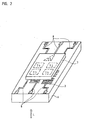
- These circuits 7.5 can be, for example, amplifiers, comparators, digitizing or interpolation circuits. In Figure 2, such a circuit 7.5 is shown schematically as an amplifier.
- a surface of the semiconductor substrate 7 has electrical connection contacts 13 which point in the direction of the carrier 6.
- electrical conductor tracks 8 are applied to the surface of the carrier 6, which have direct electrical contact with the connection contacts 13.
- the conductor tracks 8 are layers which have been evaporated, sputtered and / or electroplated by known lithography methods.
- the contacting of the connection contacts 13 with the conductor tracks 8 is preferably carried out by means of soldering, in particular reflow soldering or by means of electrically conductive adhesive.
- the connection contacts 13 are also called bonding pads and are provided with gold bumps.
- connection contacts 13 to be contacted with the conductor tracks 8 are located on the light-sensitive side of the photodetectors 7.1 to 7.4 and are thus directly opposite the conductor tracks 8. This makes it possible for all connection contacts 13 can be contacted with the conductor tracks 8 by a single method step.
- This method of contacting is in the field of electrical engineering chip on glass "under the term Flip-Chip "is known. This means that semiconductor components - that is, chips - are contacted and assembled directly and thus without a housing and without an additional carrier on a printed circuit board. This assembly is particularly stable and simple since no wire bonding is required.
- FIG. 2 shows a perspective view of the detector arrangement, consisting of the transparent carrier 6, the scanning graduation 3, the conductor tracks 8 and the semiconductor substrate 7 with the photodetectors 7.1 to 7.4 and the integrated circuit 7.5.
- the conductor tracks 8 of the carrier 6 also serve for the electrical connection to the conductor tracks 9 of a printed circuit board 10.
- the photodetectors 7.1 to 7.4 are preferably photodiodes or phototransistors. Instead of a common semiconductor substrate 7 with several photodetectors 7.1 to 7.4, several individual photodetectors can also be positioned and contacted as individual components on the carrier 6. Such individual components are shown in Figures 3 and 4.
- FIG. 3 shows a photodiode 11 with a light-sensitive pn junction and two connection contacts 13.
- FIG. 4 shows a phototransistor 12 of known construction with three connection contacts 13.
- the scanning graduation 3 is on one side of the carrier 6 and the conductor tracks 8 and the photodetectors 7.1 to 7.4 are applied on the opposite side. In not shown The scanning graduation can also be provided on the side of the conductor tracks 8.
- the scanning division 3 consists in a known manner of four groups, the divisions of the individual groups having a mutual phase offset of 90 °.
- Each group consists of a plurality of opaque lines spaced apart from one another in the measuring direction X, which faces a light-sensitive surface of a photodetector 7.1 to 7.4, 11, 12.
- the carrier 6 can also consist of transparent mylar, plastic or other transparent materials.
- the invention can be used in the case of photoelectric length or angle measuring devices, it being possible for the material measure 4 to be scanned using the transmitted light or incident light scanning method.
- the material measure 4 can be incremental or absolute.
Landscapes
- Physics & Mathematics (AREA)
- General Physics & Mathematics (AREA)
- Optical Transform (AREA)
- Length Measuring Devices By Optical Means (AREA)
- Vehicle Body Suspensions (AREA)
- Body Structure For Vehicles (AREA)
- Transmission And Conversion Of Sensor Element Output (AREA)
- Electric Double-Layer Capacitors Or The Like (AREA)
Priority Applications (1)
| Application Number | Priority Date | Filing Date | Title |
|---|---|---|---|
| DE29718469U DE29718469U1 (de) | 1996-02-08 | 1997-01-29 | Lichtelektrische Positionsmeßeinrichtung |
Applications Claiming Priority (2)
| Application Number | Priority Date | Filing Date | Title |
|---|---|---|---|
| US08598479 US5670781B1 (en) | 1996-02-08 | 1996-02-08 | Photoelectrical encoder |
| US598479 | 1996-02-08 |
Publications (3)
| Publication Number | Publication Date |
|---|---|
| EP0789228A2 true EP0789228A2 (fr) | 1997-08-13 |
| EP0789228A3 EP0789228A3 (fr) | 1999-05-12 |
| EP0789228B1 EP0789228B1 (fr) | 2004-04-07 |
Family
ID=24395702
Family Applications (1)
| Application Number | Title | Priority Date | Filing Date |
|---|---|---|---|
| EP97101330A Expired - Lifetime EP0789228B1 (fr) | 1996-02-08 | 1997-01-29 | Dispositif opto-électrique de mesure de positions |
Country Status (4)
| Country | Link |
|---|---|
| US (1) | US5670781B1 (fr) |
| EP (1) | EP0789228B1 (fr) |
| AT (1) | ATE263958T1 (fr) |
| DE (1) | DE59711485D1 (fr) |
Cited By (1)
| Publication number | Priority date | Publication date | Assignee | Title |
|---|---|---|---|---|
| DE19855828A1 (de) * | 1998-12-03 | 2000-06-08 | Heidenhain Gmbh Dr Johannes | Dreidimensionales Meßmodul |
Families Citing this family (14)
| Publication number | Priority date | Publication date | Assignee | Title |
|---|---|---|---|---|
| DE19616707A1 (de) * | 1996-04-26 | 1997-10-30 | Heidenhain Gmbh Dr Johannes | Lichtelektrische Positionsmeßeinrichtung |
| DE19855307B4 (de) | 1998-02-20 | 2005-09-29 | Dr. Johannes Heidenhain Gmbh | Abtasteinheit für eine optische Positionsmeßeinrichtung |
| DE19812008A1 (de) | 1998-03-19 | 1999-09-23 | Heidenhain Gmbh Dr Johannes | Optoelektronische Bauelementanordnung |
| DE29805392U1 (de) * | 1998-03-25 | 1999-08-05 | Dr. Johannes Heidenhain Gmbh, 83301 Traunreut | Optoelektronische Baugruppe |
| DE19854733A1 (de) * | 1998-11-27 | 2000-05-31 | Heidenhain Gmbh Dr Johannes | Abtasteinheit einer Positionsmeßeinrichtung |
| DE19859669A1 (de) | 1998-12-23 | 2000-06-29 | Heidenhain Gmbh Dr Johannes | Integrierter optoelektronischer Sensor und Verfahren zu dessen Herstellung |
| DE10033263A1 (de) | 2000-07-10 | 2002-02-28 | Heidenhain Gmbh Dr Johannes | Optische Positionsmesseinrichtung |
| US20040061044A1 (en) | 2002-09-26 | 2004-04-01 | Soar Steven E. | Techniques for reducing encoder sensitivity to optical defects |
| JP4535794B2 (ja) * | 2004-07-09 | 2010-09-01 | オリンパス株式会社 | 反射型光学式エンコーダーのセンサーヘッド |
| DE102007053137A1 (de) * | 2007-11-08 | 2009-05-14 | Dr. Johannes Heidenhain Gmbh | Abtasteinheit einer optischen Positionsmesseinrichtung und Positionsmesseinrichtung mit dieser Abtasteinheit |
| DE102008029467A1 (de) * | 2008-06-20 | 2009-12-24 | Osram Opto Semiconductors Gmbh | Halbleiterbauelement, Verwendung eines Halbleiterbauelements als Näherungssensor sowie Verfahren zum Detektieren von Objekten |
| SE537200C2 (sv) * | 2012-06-18 | 2015-03-03 | Leine & Linde Ab | Pulsgivaranordning för optisk detektering av rörelse eller läge |
| JP6383460B1 (ja) * | 2017-05-31 | 2018-08-29 | 浜松ホトニクス株式会社 | エンコーダ用受光モジュール及びエンコーダ |
| CN107255487A (zh) * | 2017-07-28 | 2017-10-17 | 上海康比利仪表有限公司 | 一种用于光电编码器的扫描装置 |
Citations (2)
| Publication number | Priority date | Publication date | Assignee | Title |
|---|---|---|---|---|
| US4840488A (en) | 1986-03-14 | 1989-06-20 | Mitutoyo Mfg. Co., Ltd. | Photoelectric type displacement detecting instrument |
| DE4006789A1 (de) | 1990-03-03 | 1991-09-05 | Zeiss Carl Fa | Optisches abtastsystem fuer rasterteilungen |
Family Cites Families (2)
| Publication number | Priority date | Publication date | Assignee | Title |
|---|---|---|---|---|
| JP3089055B2 (ja) * | 1991-08-14 | 2000-09-18 | 日本電産コパル株式会社 | 光学式変位検出装置 |
| JPH0727543A (ja) * | 1993-07-12 | 1995-01-27 | Canon Inc | 光学式変位センサー |
-
1996
- 1996-02-08 US US08598479 patent/US5670781B1/en not_active Expired - Lifetime
-
1997
- 1997-01-29 EP EP97101330A patent/EP0789228B1/fr not_active Expired - Lifetime
- 1997-01-29 AT AT97101330T patent/ATE263958T1/de not_active IP Right Cessation
- 1997-01-29 DE DE59711485T patent/DE59711485D1/de not_active Expired - Lifetime
Patent Citations (2)
| Publication number | Priority date | Publication date | Assignee | Title |
|---|---|---|---|---|
| US4840488A (en) | 1986-03-14 | 1989-06-20 | Mitutoyo Mfg. Co., Ltd. | Photoelectric type displacement detecting instrument |
| DE4006789A1 (de) | 1990-03-03 | 1991-09-05 | Zeiss Carl Fa | Optisches abtastsystem fuer rasterteilungen |
Cited By (3)
| Publication number | Priority date | Publication date | Assignee | Title |
|---|---|---|---|---|
| DE19855828A1 (de) * | 1998-12-03 | 2000-06-08 | Heidenhain Gmbh Dr Johannes | Dreidimensionales Meßmodul |
| WO2000033033A1 (fr) * | 1998-12-03 | 2000-06-08 | Dr. Johannes Heidenhain Gmbh | Module de mesure tridimensionnel |
| US6476380B1 (en) | 1998-12-03 | 2002-11-05 | Johannes Heidenhain Gmbh | Compact optical measuring module utilizing three dimensional construction |
Also Published As
| Publication number | Publication date |
|---|---|
| EP0789228A3 (fr) | 1999-05-12 |
| US5670781A (en) | 1997-09-23 |
| US5670781B1 (en) | 2000-10-10 |
| EP0789228B1 (fr) | 2004-04-07 |
| ATE263958T1 (de) | 2004-04-15 |
| DE59711485D1 (de) | 2004-05-13 |
Similar Documents
| Publication | Publication Date | Title |
|---|---|---|
| DE69715554T2 (de) | Optische Einrichtung für Verschiebungsdetektion | |
| EP0789228B1 (fr) | Dispositif opto-électrique de mesure de positions | |
| DE19523580B4 (de) | Geformte optische Verbindung | |
| DE19843155B4 (de) | Optische Verschiebungsmeßeinrichtung | |
| EP1068643A1 (fr) | Module opto-electronique | |
| DE3417176A1 (de) | Photoelektrische messeinrichtung | |
| EP0160811A2 (fr) | Dispositif de mesure photo-électrique | |
| DE19859670A1 (de) | Abtastkopf und Verfahren zu dessen Herstellung | |
| EP0401654B1 (fr) | Dispositif de couplage et/ou découplage des rayons lumineux avec élément d'optique intégré | |
| DE69729907T2 (de) | Detektionsapparat für Rotationsverschiebungsinformation | |
| DE69023266T2 (de) | Maskenkontrollierte Kopplung zwischen optischen Komponenten auf einem Substrat. | |
| EP0233594A2 (fr) | Transmetteur de position numérique | |
| DE10022676A1 (de) | Optische Verschiebungsdetektoreinrichtung | |
| DE19752511A1 (de) | Abtasteinheit für eine optische Positionsmeßeinrichtung | |
| DE10227544B4 (de) | Vorrichtung zur optischen Datenübertragung | |
| DE10058949A1 (de) | Hochgeschwindigkeits-Infrarot-Sende/Empfangs-Vorrichtung mit hohem Wirkungsgrad und niedrigen Kosten | |
| EP3124921B1 (fr) | Dispositif de mesure de position | |
| EP0101536B1 (fr) | Détecteur de mouvement relatif | |
| DE3418799C1 (de) | Inkremental-Sensor | |
| DE29718469U1 (de) | Lichtelektrische Positionsmeßeinrichtung | |
| EP1141662A1 (fr) | Module de mesure tridimensionnel | |
| DE10242027A1 (de) | Fotoelektrischer Kodierer | |
| DE19524725C1 (de) | Fotoelektrischer Kodierer zum Abtasten optischer Strukturen | |
| EP2602934B1 (fr) | Module à semi-conducteur, pilote et procédé de fabrication | |
| DE602004000174T3 (de) | Photoelektrischer Kodierer |
Legal Events
| Date | Code | Title | Description |
|---|---|---|---|
| PUAI | Public reference made under article 153(3) epc to a published international application that has entered the european phase |
Free format text: ORIGINAL CODE: 0009012 |
|
| AK | Designated contracting states |
Kind code of ref document: A2 Designated state(s): AT CH DE FR GB IT LI |
|
| PUAL | Search report despatched |
Free format text: ORIGINAL CODE: 0009013 |
|
| AK | Designated contracting states |
Kind code of ref document: A3 Designated state(s): AT CH DE FR GB IT LI |
|
| 17P | Request for examination filed |
Effective date: 19991112 |
|
| 17Q | First examination report despatched |
Effective date: 20020917 |
|
| GRAP | Despatch of communication of intention to grant a patent |
Free format text: ORIGINAL CODE: EPIDOSNIGR1 |
|
| GRAS | Grant fee paid |
Free format text: ORIGINAL CODE: EPIDOSNIGR3 |
|
| GRAA | (expected) grant |
Free format text: ORIGINAL CODE: 0009210 |
|
| AK | Designated contracting states |
Kind code of ref document: B1 Designated state(s): AT CH DE FR GB IT LI |
|
| REG | Reference to a national code |
Ref country code: GB Ref legal event code: FG4D Free format text: NOT ENGLISH |
|
| REG | Reference to a national code |
Ref country code: CH Ref legal event code: NV Representative=s name: TROESCH SCHEIDEGGER WERNER AG Ref country code: CH Ref legal event code: EP |
|
| REF | Corresponds to: |
Ref document number: 59711485 Country of ref document: DE Date of ref document: 20040513 Kind code of ref document: P |
|
| GBT | Gb: translation of ep patent filed (gb section 77(6)(a)/1977) |
Effective date: 20040518 |
|
| ET | Fr: translation filed | ||
| PLBE | No opposition filed within time limit |
Free format text: ORIGINAL CODE: 0009261 |
|
| STAA | Information on the status of an ep patent application or granted ep patent |
Free format text: STATUS: NO OPPOSITION FILED WITHIN TIME LIMIT |
|
| 26N | No opposition filed |
Effective date: 20050110 |
|
| PGFP | Annual fee paid to national office [announced via postgrant information from national office to epo] |
Ref country code: AT Payment date: 20090115 Year of fee payment: 13 |
|
| PG25 | Lapsed in a contracting state [announced via postgrant information from national office to epo] |
Ref country code: AT Free format text: LAPSE BECAUSE OF NON-PAYMENT OF DUE FEES Effective date: 20100129 |
|
| PGFP | Annual fee paid to national office [announced via postgrant information from national office to epo] |
Ref country code: IT Payment date: 20120126 Year of fee payment: 16 |
|
| PGFP | Annual fee paid to national office [announced via postgrant information from national office to epo] |
Ref country code: GB Payment date: 20130122 Year of fee payment: 17 Ref country code: CH Payment date: 20130123 Year of fee payment: 17 Ref country code: FR Payment date: 20130213 Year of fee payment: 17 |
|
| PGFP | Annual fee paid to national office [announced via postgrant information from national office to epo] |
Ref country code: DE Payment date: 20140122 Year of fee payment: 18 |
|
| REG | Reference to a national code |
Ref country code: CH Ref legal event code: PL |
|
| GBPC | Gb: european patent ceased through non-payment of renewal fee |
Effective date: 20140129 |
|
| PG25 | Lapsed in a contracting state [announced via postgrant information from national office to epo] |
Ref country code: CH Free format text: LAPSE BECAUSE OF NON-PAYMENT OF DUE FEES Effective date: 20140131 Ref country code: LI Free format text: LAPSE BECAUSE OF NON-PAYMENT OF DUE FEES Effective date: 20140131 |
|
| REG | Reference to a national code |
Ref country code: FR Ref legal event code: ST Effective date: 20140930 |
|
| PG25 | Lapsed in a contracting state [announced via postgrant information from national office to epo] |
Ref country code: FR Free format text: LAPSE BECAUSE OF NON-PAYMENT OF DUE FEES Effective date: 20140131 Ref country code: GB Free format text: LAPSE BECAUSE OF NON-PAYMENT OF DUE FEES Effective date: 20140129 |
|
| REG | Reference to a national code |
Ref country code: DE Ref legal event code: R119 Ref document number: 59711485 Country of ref document: DE |
|
| PG25 | Lapsed in a contracting state [announced via postgrant information from national office to epo] |
Ref country code: DE Free format text: LAPSE BECAUSE OF NON-PAYMENT OF DUE FEES Effective date: 20150801 |
|
| PG25 | Lapsed in a contracting state [announced via postgrant information from national office to epo] |
Ref country code: IT Free format text: LAPSE BECAUSE OF NON-PAYMENT OF DUE FEES Effective date: 20140129 |