EP0790631B1 - Elektronemittierende Vorrichtung, Elektronenstrahlerzeugungsgerät und diese Vorrichtung verwendendes Bilderzeugungsgerät - Google Patents
Elektronemittierende Vorrichtung, Elektronenstrahlerzeugungsgerät und diese Vorrichtung verwendendes Bilderzeugungsgerät Download PDFInfo
- Publication number
- EP0790631B1 EP0790631B1 EP97106945A EP97106945A EP0790631B1 EP 0790631 B1 EP0790631 B1 EP 0790631B1 EP 97106945 A EP97106945 A EP 97106945A EP 97106945 A EP97106945 A EP 97106945A EP 0790631 B1 EP0790631 B1 EP 0790631B1
- Authority
- EP
- European Patent Office
- Prior art keywords
- electron
- image
- emitting device
- forming apparatus
- voltage
- Prior art date
- Legal status (The legal status is an assumption and is not a legal conclusion. Google has not performed a legal analysis and makes no representation as to the accuracy of the status listed.)
- Expired - Lifetime
Links
- 239000010419 fine particle Substances 0.000 claims description 98
- 238000010894 electron beam technology Methods 0.000 claims description 49
- 239000000758 substrate Substances 0.000 claims description 46
- 239000000463 material Substances 0.000 claims description 45
- 229910052763 palladium Inorganic materials 0.000 claims description 13
- 239000011521 glass Substances 0.000 claims description 11
- 239000011159 matrix material Substances 0.000 claims description 8
- XOLBLPGZBRYERU-UHFFFAOYSA-N tin dioxide Chemical compound O=[Sn]=O XOLBLPGZBRYERU-UHFFFAOYSA-N 0.000 claims description 8
- 229910052751 metal Inorganic materials 0.000 claims description 5
- 239000002184 metal Substances 0.000 claims description 5
- 229910044991 metal oxide Inorganic materials 0.000 claims description 5
- 150000004706 metal oxides Chemical class 0.000 claims description 5
- 150000004767 nitrides Chemical class 0.000 claims description 5
- 239000004065 semiconductor Substances 0.000 claims description 5
- OKTJSMMVPCPJKN-UHFFFAOYSA-N Carbon Chemical compound [C] OKTJSMMVPCPJKN-UHFFFAOYSA-N 0.000 claims description 3
- 229910025794 LaB6 Inorganic materials 0.000 claims description 3
- ATJFFYVFTNAWJD-UHFFFAOYSA-N Tin Chemical group [Sn] ATJFFYVFTNAWJD-UHFFFAOYSA-N 0.000 claims description 3
- 229910052782 aluminium Inorganic materials 0.000 claims description 3
- 229910052799 carbon Inorganic materials 0.000 claims description 3
- 229910052804 chromium Inorganic materials 0.000 claims description 3
- 229910052737 gold Inorganic materials 0.000 claims description 3
- 229910052735 hafnium Inorganic materials 0.000 claims description 3
- 239000011810 insulating material Substances 0.000 claims description 3
- 229910052741 iridium Inorganic materials 0.000 claims description 3
- 229910052742 iron Inorganic materials 0.000 claims description 3
- 229910052745 lead Inorganic materials 0.000 claims description 3
- 229910052750 molybdenum Inorganic materials 0.000 claims description 3
- 229910052759 nickel Inorganic materials 0.000 claims description 3
- 229910052758 niobium Inorganic materials 0.000 claims description 3
- 229910052697 platinum Inorganic materials 0.000 claims description 3
- 229910052702 rhenium Inorganic materials 0.000 claims description 3
- 229910052703 rhodium Inorganic materials 0.000 claims description 3
- 229910052715 tantalum Inorganic materials 0.000 claims description 3
- 229910052719 titanium Inorganic materials 0.000 claims description 3
- 229910052721 tungsten Inorganic materials 0.000 claims description 3
- 230000001678 irradiating effect Effects 0.000 claims 5
- 239000002245 particle Substances 0.000 description 54
- 239000010408 film Substances 0.000 description 43
- KDLHZDBZIXYQEI-UHFFFAOYSA-N palladium Substances [Pd] KDLHZDBZIXYQEI-UHFFFAOYSA-N 0.000 description 23
- 230000000694 effects Effects 0.000 description 16
- 238000000034 method Methods 0.000 description 13
- 238000010276 construction Methods 0.000 description 12
- HBEQXAKJSGXAIQ-UHFFFAOYSA-N oxopalladium Chemical compound [Pd]=O HBEQXAKJSGXAIQ-UHFFFAOYSA-N 0.000 description 12
- 239000012789 electroconductive film Substances 0.000 description 11
- 229910003445 palladium oxide Inorganic materials 0.000 description 10
- 230000005684 electric field Effects 0.000 description 9
- 238000005259 measurement Methods 0.000 description 8
- 238000001878 scanning electron micrograph Methods 0.000 description 8
- 230000003287 optical effect Effects 0.000 description 6
- 230000007423 decrease Effects 0.000 description 5
- 239000010409 thin film Substances 0.000 description 5
- IJGRMHOSHXDMSA-UHFFFAOYSA-N Atomic nitrogen Chemical compound N#N IJGRMHOSHXDMSA-UHFFFAOYSA-N 0.000 description 3
- 239000011248 coating agent Substances 0.000 description 3
- 238000000576 coating method Methods 0.000 description 3
- UFHFLCQGNIYNRP-UHFFFAOYSA-N Hydrogen Chemical compound [H][H] UFHFLCQGNIYNRP-UHFFFAOYSA-N 0.000 description 2
- -1 TiN Chemical class 0.000 description 2
- 239000006185 dispersion Substances 0.000 description 2
- 238000010438 heat treatment Methods 0.000 description 2
- 150000002500 ions Chemical class 0.000 description 2
- 238000001000 micrograph Methods 0.000 description 2
- 239000000203 mixture Substances 0.000 description 2
- PXHVJJICTQNCMI-UHFFFAOYSA-N nickel Substances [Ni] PXHVJJICTQNCMI-UHFFFAOYSA-N 0.000 description 2
- 230000002265 prevention Effects 0.000 description 2
- 229910052709 silver Inorganic materials 0.000 description 2
- 230000003068 static effect Effects 0.000 description 2
- 229910052788 barium Inorganic materials 0.000 description 1
- 229910052792 caesium Inorganic materials 0.000 description 1
- 239000003086 colorant Substances 0.000 description 1
- 229910052802 copper Inorganic materials 0.000 description 1
- 230000007547 defect Effects 0.000 description 1
- 229910001873 dinitrogen Inorganic materials 0.000 description 1
- 238000007598 dipping method Methods 0.000 description 1
- 238000011156 evaluation Methods 0.000 description 1
- 230000001747 exhibiting effect Effects 0.000 description 1
- 239000007789 gas Substances 0.000 description 1
- 230000020169 heat generation Effects 0.000 description 1
- 239000001257 hydrogen Substances 0.000 description 1
- 229910052739 hydrogen Inorganic materials 0.000 description 1
- 238000003384 imaging method Methods 0.000 description 1
- 229910052749 magnesium Inorganic materials 0.000 description 1
- 238000000691 measurement method Methods 0.000 description 1
- 150000001247 metal acetylides Chemical class 0.000 description 1
- 150000002739 metals Chemical class 0.000 description 1
- 229910052757 nitrogen Inorganic materials 0.000 description 1
- 239000003960 organic solvent Substances 0.000 description 1
- 238000002360 preparation method Methods 0.000 description 1
- 239000010453 quartz Substances 0.000 description 1
- 239000000523 sample Substances 0.000 description 1
- VYPSYNLAJGMNEJ-UHFFFAOYSA-N silicon dioxide Inorganic materials O=[Si]=O VYPSYNLAJGMNEJ-UHFFFAOYSA-N 0.000 description 1
- 239000007787 solid Substances 0.000 description 1
- 239000000126 substance Substances 0.000 description 1
Images


Classifications
-
- H—ELECTRICITY
- H01—ELECTRIC ELEMENTS
- H01J—ELECTRIC DISCHARGE TUBES OR DISCHARGE LAMPS
- H01J1/00—Details of electrodes, of magnetic control means, of screens, or of the mounting or spacing thereof, common to two or more basic types of discharge tubes or lamps
- H01J1/02—Main electrodes
- H01J1/30—Cold cathodes, e.g. field-emissive cathode
- H01J1/316—Cold cathodes, e.g. field-emissive cathode having an electric field parallel to the surface, e.g. thin film cathodes
-
- B—PERFORMING OPERATIONS; TRANSPORTING
- B82—NANOTECHNOLOGY
- B82Y—SPECIFIC USES OR APPLICATIONS OF NANOSTRUCTURES; MEASUREMENT OR ANALYSIS OF NANOSTRUCTURES; MANUFACTURE OR TREATMENT OF NANOSTRUCTURES
- B82Y10/00—Nanotechnology for information processing, storage or transmission, e.g. quantum computing or single electron logic
-
- H—ELECTRICITY
- H01—ELECTRIC ELEMENTS
- H01J—ELECTRIC DISCHARGE TUBES OR DISCHARGE LAMPS
- H01J31/00—Cathode ray tubes; Electron beam tubes
- H01J31/08—Cathode ray tubes; Electron beam tubes having a screen on or from which an image or pattern is formed, picked up, converted, or stored
- H01J31/10—Image or pattern display tubes, i.e. having electrical input and optical output; Flying-spot tubes for scanning purposes
- H01J31/12—Image or pattern display tubes, i.e. having electrical input and optical output; Flying-spot tubes for scanning purposes with luminescent screen
- H01J31/123—Flat display tubes
- H01J31/125—Flat display tubes provided with control means permitting the electron beam to reach selected parts of the screen, e.g. digital selection
- H01J31/127—Flat display tubes provided with control means permitting the electron beam to reach selected parts of the screen, e.g. digital selection using large area or array sources, i.e. essentially a source for each pixel group
-
- H—ELECTRICITY
- H01—ELECTRIC ELEMENTS
- H01J—ELECTRIC DISCHARGE TUBES OR DISCHARGE LAMPS
- H01J2201/00—Electrodes common to discharge tubes
- H01J2201/30—Cold cathodes
- H01J2201/316—Cold cathodes having an electric field parallel to the surface thereof, e.g. thin film cathodes
- H01J2201/3165—Surface conduction emission type cathodes
-
- H—ELECTRICITY
- H01—ELECTRIC ELEMENTS
- H01J—ELECTRIC DISCHARGE TUBES OR DISCHARGE LAMPS
- H01J2329/00—Electron emission display panels, e.g. field emission display panels
- H01J2329/86—Vessels
- H01J2329/8625—Spacing members
-
- H—ELECTRICITY
- H01—ELECTRIC ELEMENTS
- H01J—ELECTRIC DISCHARGE TUBES OR DISCHARGE LAMPS
- H01J2329/00—Electron emission display panels, e.g. field emission display panels
- H01J2329/86—Vessels
- H01J2329/8625—Spacing members
- H01J2329/863—Spacing members characterised by the form or structure
Definitions
- the present invention relates to a cold-cathode type of electron-emitting device.
- the present invention also relates to an electron beam-generating apparatus, and an image-forming apparatus employing the electron-emitting device.
- Cold cathode devices are known as devices capable of emitting electrons with a simple structure.
- a cold cathode device is reported by M.I. Elinson (Radio Eng. Electron Phys., vol. 10, pp. 1290-1296 (1965)). These devices are based on the phenomenon that electrons are emitted by flowing electric current in parallel through a thin film of small area formed on a substrate. Such devices are called generally surface-conduction type electron-emitting devices.
- the surface-conduction type electron-emitting devices include the ones using a thin SnO 2 (Sb) film developed by M.I. Elinson as mentioned above; the ones using a thin Au film (G. Dittmer: "Thin Solid Films", vol. 9, p. 317, (1972)); and the ones using a thin ITO film (M. Hartwell and C.G. Fonstad: IEEE Trans. ED Conf., p. 519 (1975)).
- FIG. 30 A typical construction of the surface conduction type electron-emitting device is shown in Fig. 30.
- This device comprises electrodes 82, 83 for electric connection, a thin film 85 formed from an electron-emitting material, a substrate (insulating base) 81, and an electron-emitting portion 84.
- the electron-emitting portion is formed by electric current-heating treatment called "forming".
- forming electric current-heating treatment
- electric voltage is applied between the electrode 82 and the electrode 83 to flow electric current through the thin film 85 and to destroy, deform, or denature locally the thin film 85 by utilizing Joule heat generated.
- the electron-emitting portion 84 which has high electric resistance is formed, thus the function of electron emission being obtained.
- the state of the high electric resistance results from discontinuity of the thin film 85 in which cracks of 0.5 to 5 ⁇ m long are formed locally and the cracks have an island structure therein.
- the island structure means a state of the film that the film contains fine particles of several tens of angstroms to several microns in diameter and the particles are discontinuous but the film is electrically continuous.
- voltage is applied to the aforementioned discontinuous high-resistance film through the electrodes 82, 83 to flow current at the surface of the device, thereby electron being emitted from the fine particles.
- a novel surface conduction type electron-emitting device in which electron-emitting fine particles are distributed between electrode was disclosed by the inventors of the present invention in Japanese Patent Application Laid-Open Nos. Hei-1-200532 and Hei-2-56822.
- This electron-emitting device has advantages that (1) high electron-emitting efficiency can be obtained, (2) the device can be readily prepared because of its simple construction, (3) many devices can be arranged on one and the same substrate, and so forth.
- Fig. 31 shows a typical construction of such a surface conduction type electron-emitting device, which comprises electrodes 82, 83 for electric connection, an electron-emitting portion 86 having electron-emitting fine particles dispersed therein, and a substrate 81.
- Fig. 32 illustrates an image-forming apparatus having a number of the aforementioned electron-emitting devices arranged therein.
- the apparatus comprises wiring electrodes 92, 93, electron-emitting portions 94, grid electrodes 95, electron-passing holes 96, and an image-forming member 97.
- This image-forming member is made of a material such as fluorescent materials and resist materials which causes light-emission, color change, electrification, denaturing or like change on collision of electrons.
- the linear electron sources having a plurality of electron-emitting portions 94 arranged between the electrodes 92, 93, and grid electrodes 95 are driven in XY matrix, and electrons are made to collide against the image-forming member 97 in correspondence with information signals to form an image.
- the electric characteristics (current-voltage characteristics) of conventional surface conduction type of electron-emitting devices are explained by reference to Fig. 6.
- electron emission increases rapidly from a certain device voltage Ve (voltage applied to the device) with increase of the device voltage, and at a device voltage Vd, sufficient electron beam comes to be emitted: for example, sufficient electron beam for forming image in the above-mentioned image-forming apparatus.
- the device current If (current which flows in the device) increases with the device voltage, and the rate of the increase becomes larger at around the device voltage Ve.
- strong ineffective current which is useless for electron emission, flows as shown in Fig. 6.
- the ratio of the ineffective current to the device current If rises in some cases to as much as about 50 %. Such increase of the ineffective current will cause increase of power consumption in driving the electron-emitting device, and increase of heat generation in the electron-emitting device to deteriorate electron-emitting characteristics (electron-emission efficiency, electron-emission stability, etc.
- the ineffective current gives rise to the problems, when the electron-emitting device in which the ineffective current is remarkable is used for an image-forming apparatus: 1) the ineffective current flows to wiring electrodes to cause voltage drop, whereby the quantity of electron emission varies with the electron-emitting devices, and 2) the ineffective current varies depending on the kind of the image (namely, difference in inputted information signal) to cause voltage drop in wiring electrode, whereby quantity of the emitted electrons varies.
- Such disadvantageous phenomena further cause lowering of contrast and sharpness of the formed image; and in particular, in the case where the formed image is a fluorescent image, bring about variation and change of luminance of the fluorescent images, which makes it difficult to obtain fineness of the image and to enlarge a picture screen, and further increase the power consumption.
- An object of the present invention is to provide an electron-emitting device and an electron beam-generating apparatus in which ineffective current is extremely weak.
- Another object of the present invention is to provide an electron-emitting device and an electron beam-generating apparatus which are excellent in electron emission characteristics such as electron-emission efficiency, and electron-emission stability, and which consumes less electric power.
- a further object of the present invention is to provide an electron beam-generating apparatus in which ineffective current is extremely weak in a whole apparatus, and which gives an image with high contrast and high sharpness with less power consumption, in particular an electron beam-generating apparatus capable of forming a luminescent image with extremely low variation and low fluctuation of luminance.
- an electron-emitting device having an electron-emitting region between electrodes on a substrate, the voltage application length in the electron-emitting region ranging from 0,5 to 30 nm for an applied voltage of 1,0 to 4.0 V.
- an electron-emitting device having an electron-emitting region between electrodes on a substrate, the electric field strength in the electron-emitting region being not less than 10 7 V/cm when voltage for releasing electrons is applied.
- an electron-beam generating apparatus comprising a plurality of the above-specified electron-emitting devices and a modulation means for modulating the electron beams emitted from the electron-emitting devices in accordance with information signals.
- an image-forming apparatus comprising a plurality of the above-specified electron-emitting devices, a modulation means for modulating the electron beams emitted from the electron-emitting devices in accordance with information signals, and an image-forming member for forming image on irradiation of electron beams.
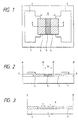
- Fig. 1 is a plan view illustrating schematically an electron-emitting device of the present invention.
- Fig. 2 is a sectional view of the electron-emitting device at A-A' in Fig. 1.
- Fig. 3 is a sectional view of the electron-emitting device at B-B' in Fig. 2.
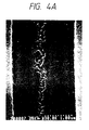
- Fig. 4A is an SEM photograph of an electron-emitting region between electrodes of an electron-emitting device of the present invention (magnification: ⁇ 30,000).
- Fig. 4B is a sketch of an SEM photograph of an electron-emitting region of Fig. 4A (plan view).
- Fig. 5A is an enlarged SEM photograph of an electron-emitting region of the electron-emitting device of Fig. 4 (magnification: ⁇ 150,000).
- Fig. 5B is an enlarged SEM photograph of an electron-emitting region of the electron-emitting device of Fig. 4 (magnification: ⁇ 800,000).
- Fig. 5C is a sketch of the enlarged SEM photograph of an electron-emitting region of Fig. 5A (plan view).
- Fig. 6 shows current-voltage relation of a conventional electron-emitting device.
- Fig. 7 shows current-voltage relation of an electron-emitting device of the present invention.
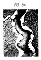
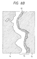
- Fig. 8A is an SEM photograph (magnification: ⁇ 150,000) to explain the method for measuring the voltage application length of the electron-emitting device of the present invention.
- Fig. 8B is a sketch of the SEM photograph of Fig. 8A.
- Fig. 9A is another SEM photograph (magnification: ⁇ 150,000) to explain the method for measuring the voltage application length of the electron-emitting device of the present invention.
- Fig. 9B is a sketch of the SEM photograph of Fig. 9A.
- Fig. 10 is a drawing to explain the method for measuring the voltage application length of the electron-emitting device of the present invention.
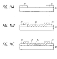
- Figs. 11A to 11C are drawings to explain a method for preparing the electron-emitting device of the present invention (sectional view).
- Fig. 12 shows a wave form of the pulse voltage on forming treatment of an electron-emitting device of the present invention.
- Fig. 13 shows another wave form of the pulse voltage on forming treatment of an electron-emitting device of the present invention.
- Figs 14A to 14E are drawings to explain a method for preparing the electron-emitting device of the present invention (sectional view).
- Figs. 15A to 15D are drawings to explain a method for preparing the electron-emitting device of the present invention (sectional view).
- Fig. 16 illustrates schematically the construction of the measurement apparatus of electron emission characteristics of an electron-emitting device.
- Fig. 17 is a perspective view illustrating schematically an electron beam-generating apparatus of the present invention.
- Fig. 18 is a perspective view illustrating schematically another electron beam-generating apparatus of the present invention.
- Fig. 19 is a perspective view illustrating schematically still another electron beam-generating apparatus of the present invention.
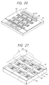
- Fig. 20 is a perspective view illustrating schematically still another electron beam-generating apparatus of the present invention.
- Fig. 21 is a perspective view illustrating schematically still another electron beam-generating apparatus of the present invention.
- Fig. 22 is a perspective view illustrating schematically an image-forming apparatus of the present invention.
- Fig. 23 is a perspective view illustrating schematically another image-forming apparatus of the present invention.
- Fig. 24 is a perspective view illustrating schematically still another image-forming apparatus of the present invention.
- Fig. 25 is a perspective view illustrating schematically still another image-forming apparatus of the present invention.
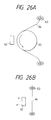
- Figs. 26A and 26B illustrate schematically an image-forming apparatus (optical printer) of the present invention.
- Fig. 27 illustrates schematically another image-forming apparatus (optical printer) of the present invention.
- Fig. 28 illustrates schematically an image forming apparatus provided with a supporting member of the present invention (assembling drawing).
- Fig. 29 is a sectional view of the apparatus of Fig. 28.
- Fig. 30 is a plan view illustrating schematically construction of a conventional electron-emitting device.
- Fig. 31 is a plan view illustrating schematically construction of another conventional electron-emitting device.
- Fig. 32 is a perspective view of a conventional image-forming apparatus.
- Fig. 1 plan view
- Fig. 2 sectional view at A-A' in Fig. 1
- Fig. 3 sectional view at B-B' in Fig. 2).
- the numeral 1 denotes an insulating substrate; 2 and 3, each an electrode; 5, an electron-emitting region; 4, a fine particle film having an electric resistance lower than that of the electron-emitting region 5; and 6, a fine particle dispersed in the electron-emitting region 5.
- the electron-emitting device of the present application is required essentially to have an electron-emitting region 5 having fine particles 6 dispersed therein, and electrodes 2 and 3 to apply voltage to the interior of the region 5.
- the electron-emitting device of the present application serves in such a mechanism that electrons pass (or current flows) through the electron-emitting region by application of voltage between the electrodes 2 and 3, and the electrons are emitted out from the gap formed by the fine particles 6 (or spacing between the fine particles) in the region.
- the fine particle film 4 having lower resistance is not an essential requirement in the present invention, but is preferred to improve further the electrical contact between the electron-emitting region 5 and the electrodes 2 and 3.
- the electron-emitting region and the fine particles constituting the fine particle film 4 are both made of an electroconductive material.
- the electron-emitting device of the present application has to satisfy further another requirement shown below, and is classified into two types of embodiments according to the requirement. It is described in detail.
- the areal occupation ratio of of the fine particles is in the range of from 20 to 75 % in the electron-emitting region 5.
- Fig. 4A, Fig. 5A, and Fig. 5B are SEM (scanning electron microscope) photographs of an electron-emitting region of an electron-emitting device of the present application prepared as examples described later.
- Fig. 4B and Fig. 5C are sketches of the SEM photographs.
- Fig. 4A and Fig. 4B shows a view of the region A-A' of Fig. 2 observed from the top.
- Fig. 5A and Fig. 5C shows a view of the region A-A' of Fig. 2 observed from the top.
- the areal occupation ratio in the present invention means the value measured as follows. As shown by the dotted-line area in Fig. 5C, the SEM image of the inside of the electron-emitting region 15 of the element is taken at a magnification such that 10 to 1000 fine particles are observed (Fig. 5B).
- the relations of the areal occupation ratio of the fine particles with the aforementioned ineffective current flowing in the device, and with the electron-emitting characteristics of the device are considered as below by the inventors of the present invention. If the areal occupation ratio of the fine particles is excessively large, the ratio of the aforementioned gap to the entire electron-emitting region is extremely small, and the the electron-emitting region behaves as a continuous film. Therefore, the quantity of electrons flowing through the continuous film is larger than the quantity of electrons emitted from the gap. As the results, the the ineffective current becomes stronger, and quantity of the emitted electrons decreases.
- the areal occupation ratio of the fine particles is in the range of from 20 to 75 %, more preferably from 35 to 60 %, the ineffective current of the electron-emitting device is effectively made extremely small, and the quantity of electron emission is increased, and further thereby the electron-emission efficiency and the electron-emission stability are improver effectively. Consequently, the present application has been completed.
- the average particle diameter of the fine particles dispersed in the electron-emitting region is adjusted preferably to be in the range of from 5 to 300 ⁇ , more preferably 5 to 80 ⁇ . With the average diameter within this range, the ineffective current flowing through very large particles can be suppressed, the ineffective current in the whole device can further be reduced, and the electron emission efficiency and the electron emission stability (in particular, flickering of electron emission) are improved more.
- the gap between the fine particles 6 in the electron-emitting region 5 is in the range of from 5 to 100 ⁇ , and the average particle diameter of the fine particles is in the range of from 5 to 1000 ⁇ .
- the gap between the fine particles in the present invention means the spacing of particles as shown by the symbol S in Fig. 3.
- the gap S of the fine particles and the average particle diameter t are measured as follows. As shown by the dotted-line area in Fig. 5, the SEM image of the inside of the electron-emitting region 15 (photograph) of the element is taken at a magnification such that 10 to 1000 fine particles are observed.
- the dependence of the ineffective current flowing in the device and the electron emission characteristics of the device on the fine particle gap and the average diameter are considered as below by the inventors. If the average particle diameter is excessively large and the fine particle gap is extremely small, the ratio of the aforementioned gap to the entire electron-emitting region is too small, and the the electron-emitting region behaves as a continuous film. Therefore, the quantity of electrons flowing through the continuous film is larger than the quantity of electrons emitted from the gap. As the results, the the ineffective current becomes large, and quantity of the emitted electrons decreases.
- the average particle diameter is extremely small and the gap of the fine particles is extremely large, the ratio of the aforementioned gap to the entire electron-emitting region is too large, and the higher voltage is required for electron emission. Therefore, a phenomenon occurs that electrons once emitted are pulled back to the electrode. As the results, the ineffective current becomes large, and the quantity of the emitted electrons decreases also in this case.
- the gap of the fine particles is adjusted to be within the range of from 5 to 100 ⁇ , preferably 5 to 50 ⁇ , the ineffective current of the electron-emitting device is effectively made extremely small, and the quantity of electron emission is increased, and further thereby the electron emission efficiency and the electron emission stability are improved effectively. Consequently, the present invention has been completed.
- the average particle diameter of the fine particles dispersed in the electron-emitting region is adjusted preferably to be in the range of from 5 to 300 ⁇ , more preferably 5 to 80 ⁇ from the same reason as in the above-described first embodiment.
- the electron-emitting device which meets simultaneously the both requirements of the two types of embodiments is more preferable. That is, if the areal occupation ratio in the electron-emitting region is from 20 to 75 %, the gap of the particles is from 5 to 100 ⁇ , and the average particle diameter of the fine particles is from 5 to 1000 ⁇ , then the electron-emitting device is improved in comparison with each of the above embodiments in reducing the ineffective current in the device and is superior in electron emission quantity, electron emission efficiency, and electron emission stability (prevention of flickering of electron emission), and further the device is driven with lower voltage and has longer life.
- the above effects are more remarkable if the areal occupation ratio is from 35 to 60 %, and the particle gap is from 5 to 50 ⁇ .
- the effects are still more remarkable if the average particle diameter is from 5 to 300 ⁇ , more preferably 5 to 80 ⁇ .
- the methods for controlling the areal occupation ratio, the fine particle gap, and the fine particle diameter are described below.
- the control of these parameters were practiced as follows.
- the gap between the electrodes was set in the range of from 0.2 to 5 ⁇ m.
- An electroconductive film having sheet resistance of from 3 ⁇ 10 3 ⁇ /cm 2 to 10 7 ⁇ /cm 2 was formed by placing electroconductive particles of from 5 to 100 ⁇ in particle diameter in dispersion between the electrodes.
- a specified wave form of voltage pulse was applied through the electrodes.
- the applied voltage pulse is suitably decided depending on the shape of the electrodes, the material of the electroconductive film, and the material of the substrate.
- the material of the electroconductive particles includes metals such as Pd, Nb, Mo, Rh, Hf, Ta, W, Re, Ir, Pt, Ti, Au, Ag, Cu, Cr, Al, Co, Ni, Fe, Pb, Cs, and Ba; borides such as LaB 6 , CeB 6 , HfB 4 , and GdB 4 ; carbides such as TiC, ZrC, HfC, TaC, SiC, and WC; nitrides such as TiN, ZrN, and HfN; metal oxides such as PdO, Ir 2 O 3 , SnO 2 , and Sb 2 O; semiconductors such as Si, and Ge; carbon, Ag, Mg, and the like.
- the above method is preferred in controlling the parameters.
- the large ineffective current of conventional electron-emitting device as described above was further studied by the inventors of the present invention. As the results, it was found that the strength of the ineffective current flowing through the electron-emitting device varies depending on the size of the region where the voltage for driving the device is effectively applied (the size being referred to as "voltage application length"). It was further found that the ineffective current can be suppressed to extremely small by adjusting the voltage application length within a certain range, the ineffective current of the device being negligible at the voltage application length of from 5 to 300 ⁇ , preferably 5 to 50 ⁇ .
- the voltage application length in more detail, means a length of the region where the voltage is effectively applied as described above in the electron-emitting device. In this region, voltage drops substantially but outside the region, the voltage does not drop substantially.
- Fig. 8A is an SEM photograph of an area between the electrodes on application of voltage to an electron-emitting device of the present invention.
- Fig. 8B is a sketch of the SEM photograph of Fig. 8A.
- Fig. 9A is an SEM photograph of an area between the electrodes of the same electron-emitting device on application of voltage in the reversed direction.
- Fig. 9B is a sketch of the SEM photograph of Fig. 9A. In Fig 8B and Fig.
- the numeral 15 denotes an electron-emitting region
- the numeral 14 denotes an electroconductive film for sufficient electric contact of electrodes (not shown in the drawing) with the electron-emitting region
- the numeral 17 denotes a portion from which the secondary electron emission is less. This portion is observed to be dark in the actual SEM image (Fig. 8A and Fig. 9B).
- the SEM photograph of the area between the device electrodes to be measured is taken by applying to the electrodes a voltage of from 1.5 V to 4.0 V under a vacuum of from 1 ⁇ 10 -3 to 1 ⁇ 10 -6 torr (1,333 ⁇ 10 -6 to 1,333 ⁇ 10 -9 bar).
- the same SEM, photograph is taken by applying the same voltage in the reversed direction at the same magnification.
- the obtained two SEM images are superposed as shown in Fig. 10.
- the maximum width L of the blank area 18 in the electron-emitting region 15 is measured, from which the real length is calculated in consideration of the magnification of the SEM.
- STM may be employed for measurement.
- a voltage of 1 to 2.5 V is applied to the device, and the probe of the STM is driven to scan the area to be measured from the negative potential side to the positive potential electrode side.
- the length of the region where 30 % to 70 % of the applied voltage is observed is taken as the voltage application length.
- the control of the voltage application length and the electric field strength of the electron-emitting device was practiced as below.
- the gap between the electrodes was set in the range of from 0.2 to 5 ⁇ m.
- An electroconductive film having sheet resistance of from 3 ⁇ 10 3 ⁇ /square to 10 7 ⁇ /square was formed.
- a specified wave form of voltage pulse was applied through the electrodes.
- the applied voltage pulse is suitably decided depending on the shape of the electrodes, the material of the electroconductive film, and the material of the substrate.
- the electroconductive film is preferably formed, as described later in Examples, by placing electroconductive particles of from 5 to 1000 ⁇ in particle diameter in dispersion between the electrodes, the material thereof is those mentioned above.
- the electron-emitting devices of the above embodiments of the present invention exhibit extremely small ineffective current, the ineffective current being 2% or less, in more preferred embodiment, 1 % or less.
- the electron-emitting device of any embodiment of the present invention is excellent in electron-emitting characteristics such as electron emission quantity, electron emission efficiency, and emission stability (prevention of flickering of electron emission).
- the electron beam-generating apparatus and the image-forming apparatus of the present invention are described below in detail.
- the electron beam-generating apparatus and the image-forming apparatus of the present invention are characterized by use of the above-described electron-emitting devices.
- the electron beam-generating apparatus of the present invention comprises a plurality of the above electron-emitting devices, and modulation means for modulating electron beams emitted from the electron-emitting devices in accordance with information signals.
- the numeral 41 denotes an insulating substrate; 42 and 43, electrodes; 45, an electron-emitting region; 44, an electroconductive film for obtaining sufficient electric contact between the electrode and the electron-emitting region; and 46, a modulation means.
- linear electron-emitting devices having a plurality of electron-emitting regions are juxtaposed on the substrate, and a plurality of grid electrodes (modulation electrodes) 46 are placed in an XY matrix with the linear electron-emitting devices.
- the grid electrodes are placed above the electron-emitting face of the electron-emitting device in Fig. 18; juxtaposed on the same substrate plane as the electron-emitting devices in Fig.
- a plurality of electron-emitting devices having each a single electron-emitting portion are arranged in matrix, and each element is connected to a signal wiring electrode 50 and a scanning wiring electrode 51 as shown in the drawing.
- This construction is called a simple matrix construction, in which the signal wiring electrodes 50 and the scanning wiring electrodes 51 serves as the modulation means.
- the electron beam-generating apparatuses exemplified above are driven as below. To drive the apparatus illustrated in Fig.
- pulsing voltage of 10 to 35 V is applied to the electrodes 42 and 43 of one line of the linear electron-emitting devices to cause emission of electron beams from a plurality of the electron-emitting portions.
- the emitted electron beams are turned on and off by application of voltage of from 50 V to -70 V to the grid electrodes 46 in correspondence with information signals to obtain electron emission corresponding the information signals for the one line. Such operation is conducted sequentially for the adjacent lines of the linear electron-emitting devices to obtain electron beam emission for one picture image.
- pulsing voltage is applied with the scanning wiring electrode 51 to the plurality of the electron-emitting devices on one line, and subsequently pulsing voltage is applied to the signal wiring electrodes 50 in correspondence with information signals to obtain electron emission corresponding to information signal for one line. Such operation is conducted sequentially for adjacent lines to obtain electron beam emission for one picture image.
- the electron beam-generating apparatus of the present invention is advantageous in that the ineffective current in the whole apparatus is extremely week, electron-emitting characteristics such as electron emission efficiency and electron emission stability are excellent, and power consumption is low.
- the image-forming apparatus of the present invention has a constitution such that an image-forming member is placed on the electron beam emission side of the aforementioned electron beam-generating apparatus.
- the image-forming member is constituted of a material which causes light emission, color change, electrification, denaturing, etc. on collision of electrons, such as a light-emitting material like a fluorescent material, and a resist material.
- Fig. 22 illustrates one embodiment of an image-forming apparatus of the present invention.
- the apparatus of Fig. 22 comprises a rear plate 52 (which may serve also as the aforementioned insulating substrate 41), modulation means 46 (which are shown in a form of grid electrodes of Fig. 18, but may be the grid electrodes of Fig.
- Electrodes 42 and 43 electrodes 42 and 43, electron-emitting regions 45, electroconductive films 44 for obtaining sufficient electric contact between the electrodes and the electron-emitting regions, a face plate 58, a glass plate 57, a transparent electrode 55, and a fluorescent material 56.
- voltage of from 0.5 KV to 10 KV is applied to the image-forming member (transparent electrode 55 in Fig. 22), and then the apparatus is driven in the same manner as driving of the above-described electron beam-generating apparatus, thus an image corresponding to information signals being obtained on the image-forming member (fluorescent image in Fig. 22).
- the image-forming member is made of a light-emitting material such as a fluorescent material
- a full-color image display can be obtained by using three light-emitting materials of three primary colors of red, green, and blue for one picture element.
- the electron beam-generating apparatus and the image-forming apparatus described above are usually driven at a vacuum of 10 -4 to 10 -9 torr.
- the image-forming apparatus of the present invention includes the embodiment shown in Fig. 28 and Fig. 29.
- a supporting member for supporting the atmospheric pressure is provided between the face plate 58 and the rear plate 52 in the image-forming apparatus of Fig. 23, Fig. 24, or Fig. 25.
- Fig. 28 illustrates schematically the construction of an image-forming member of the present invention.
- Fig. 29 is a sectional view of the image-forming apparatus viewed at around the atmospheric pressure-supporting member of the image-forming apparatus shown in Fig 28.
- the numeral 95 denotes an atmospheric pressure-supporting member; 96, a supporting frame; and 97, a luminescent spot of the fluorescent substance.
- An envelop of the image-forming apparatus is constructed of a face plate 58, a rear plate 52, and a supporting frame 96.
- the internal pressure is kept at a vacuum of 10 -4 to 10 -9 torr.
- an atmospheric pressure-supporting member is provided desirably.
- the atmospheric pressure-supporting members 95 are placed usually at intervals of from 1 mm to 100 mm between the picture elements so that image defect may be avoided.
- the material of the atmospheric pressure-supporting member 95 is an insulating material such as glass.
- the supporting member When the image-forming apparatus having an atmospheric supporting member 95 as shown in Fig. 28 and Fig. 29 is driven, the supporting member is liable to be electrically charged by unexpected collision of electron beam or ions against the supporting member 95 since the supporting member 95 is electrically floating.
- This electric charging bends the locus of the electron beam and changes the amount of the electron beam colliding to the fluorescent material, causing irregularity of luminance and color.
- the disadvantage caused by the electric charging of the supporting member relates to driving voltage of the electron-emitting device. If the ineffective current of the electron-emitting device is large, the voltage applied to the device is high, and the supporting member 95 becomes liable to be charged. Accordingly, in the present invention, use of an electron-emitting device causing weak ineffective current makes it possible to obtain image-forming apparatus with large picture area and light weight.
- the image-forming apparatus of the present invention includes the embodiments shown in Fig. 26 and Fig. 27, which are examples of optical printers employing as the light source the image-forming apparatus illustrated in Fig. 22.
- the numeral 62 denotes the light source; 65 a drum; 63, a delivery roller; and 64, a heat-sensitive or light-sensitive sheet.
- the optical printer records image on a recording medium by driving the light source as described above (as driving of the image-forming apparatus of Fig. 22) to emit light in correspondence with information signals onto the recording medium 64 with scanning of the recording medium 64 supported by a support 65 or 63, or the light source 62.
- Fig. 27 illustrates another embodiment of the optical printer.
- the numeral 71 denotes a light source; 72, a drum-shaped recording medium; 77, a developer; 75, a static eliminator; 74, a cleaner; 73, an electric charger; and 76, an image-transfer medium.
- This optical printer records an image by electrically charging the recording medium 72 with an electric charger 73, projecting light beam emitted from the light source 71 in a manner as above (driving method of the image-forming apparatus of Fig. 22) to the recording medium 72 to eliminate electric charge from the illuminated area, adhering a toner on the non-illuminated area by means of a developer 77, and transferring the toner onto the image-transfer medium 76 by eliminating the electric charge at the position of the static eliminator 75.
- the image-forming apparatus of the present invention as described above is capable of forming image with high contrast and sharpness with less consumption of electric power.
- the image-forming apparatus utilizing luminescent image gives extremely small variation or flickering of the luminance.
- Electron-emitting devices of the type shown in Figs. 1 to 3 were prepared. The procedure of the preparation is described below by reference to Fig. 11.
- the pulse width T 1 was 1.0 millisecond, and the pulse interval T 2 was 10 milliseconds in this Example.
- the forming treatment was conducted at the forming voltage as shown below. under a vacuum environment of about 1 ⁇ 10 -6 torr.
- the electron-emitting region 25 was formed between the fine palladium oxide film 4, and was composed of fine palladium particles 6 as shown in Fig. 3.
- the fine particles 6 had an average diameter of 10 ⁇ .
- Three devices of different areal occupation ratio of the fine particles 6 were prepared by changing the amount of the coating of the organic palladium to change a sheet resistance of the fine particle film 24 in the step (2) and changing the forming voltage in the step (3).
- Fig. 16 illustrates schematically the construction of the measuring apparatus.
- the measuring apparatus comprises an insulating substrate 21, electrodes 22 and 23, an electron-emitting region 25, electroconductive films 24 for obtaining electric contact, a power source 31 for applying voltage to the device, an ammeter 30 for measuring the device current (If), an anode electrode 34 for measuring emission current (Ie) emitted from the device, a high-voltage power source 33 for applying voltage to the anode electrode 34, and an ammeter 32 for measuring the emission current.
- the aforementioned device current means the current measured by the ammeter 30, and the emission current means the current measured by the ammeter 32.
- Electron-emitting devices were prepared by the procedure below.
- Two kinds of devices were prepared by changing the voltage in the forming treatment.
- An electron-emitting device was prepared in the same manner as in Example 2 except that the sheet resistance of the fine particle film 24 was 5 ⁇ 10 5 ⁇ /square and the forming voltage was 4 V. In the resulting device, the areal occupation ratio of the fine particles 6 was 50 %, and the average particle diameter of the fine particles 6 was 5 ⁇ . The electron-emitting device exhibited approximately the same effect as the ones in Example 2 (ineffective current being not more than 1 %).
- Electron-emitting devices were prepared as below.
- Three kinds of devices were prepared by changing the amount of the coating of the organic palladium to change the sheet resistance of the fine particle film 24 and by changing the forming voltage as below:
- An electron-emitting device was prepared in the same manner as in Example 4 except that the sheet resistance of the fine particle film 24 was 1 ⁇ 10 5 ⁇ /square and the forming voltage was 4 V. In the resulting device, the average particle gap was 5 ⁇ , and the average particle diameter was 50 ⁇ . The electron-emitting device exhibited approximately the same effect as the ones in Example 4 (ineffective current being not more than 3 %).
- An electron-emitting device was prepared in the same manner as in Example 4 except that the sheet resistance of the fine particle film 24 was 5 ⁇ 10 3 ⁇ /square and the forming voltage was 14 V. In the resulting device, the average particle gap was 100 ⁇ , and the average particle diameter was 50 ⁇ . The electron-emitting device exhibited approximately the same effect as the ones in Example 4 (ineffective current being not more than 1 %).
- Electron-emitting devices were prepared as below.
- Two kinds of devices were prepared by changing the amount of coating to change the sheet resistance of the fine particle film 24, and by changing the forming voltage.
- An electron-emitting device was prepared in the same manner as in Example 7 except that the sheet resistance of the fine particle film 24 was 3 ⁇ 10 5 ⁇ /square and the forming voltage was 4 V. In the resulting device, the average particle gap was 30 ⁇ , and the average particle diameter was 5 ⁇ . The electron-emitting device exhibited approximately the same effect as the ones in Example 7 (ineffective current being not more than 1.0 %).
- Electron-emitting devices were prepared as below. The procedures explained by reference to Fig. 14.
- Figs. 14A to 14C were practiced in the same manner as in the steps (1) to (3) in Example 1 except that the forming treatment was conducted with the voltage wave form as shown in Fig. 12 at the forming voltage of 8 V, the pulse width of T 1 of 1 millisecond, and the pulse interval T 2 of 10 milliseconds.
- An electron-emitting device was prepared in the.same manner as in Example 9 except that the steps (4) and (5) were conducted four times.
- the areal occupation ratio of the of the fine particles in the electron-emitting region was 75 %
- the average particle diameter of the fine particles was 35 ⁇
- the average gap of the fine particles was 5 ⁇ .
- the device was evaluated in the same manner as in Example 9. The effect was nearly the same as that of Example 9 (ineffective current: not more than 2.0 %).
- An electron-emitting device was prepared in the same manner as in Example 9 except that in the step (4) the forming voltage was 12 V.
- the areal occupation ratio of the fine particles in the electron-emitting region was 20 %
- the average particle diameter of the fine particles was 25 ⁇
- the average gap of the fine particles was 100 ⁇ .
- the device was evaluated in the same manner as in Example 9. The effect was nearly the same as that of Example 9 (ineffective current: not more than 0.2 %).
- An electron-emitting device was prepared in the same manner as in Example 9 except that in the step (4) the forming voltage was 12 V, and the steps (4) and (5) were conducted twice.
- the areal occupation ratio of the of the fine particles in the electron-emitting region was 50 %
- the average particle diameter of the fine particles was 300 ⁇
- the average gap of the fine particles was 30 ⁇ .
- Example 9 The device was evaluated in the same manner as in Example 9. The effect was nearly the same as that of Example 9 (ineffective current: not more than 1.0 %).
- Electron-emitting devices were prepared as below. The procedures explained by reference to Fig. 15.
- An electron ray-generating apparatuses were prepared by arranging in a line a plurality of the electron-emitting devices prepared in Examples 1 - 13 as shown in Fig. 17.
- the apparatus comprises an insulating substrate (a rear plate) 41, wiring electrodes 42 and 43, low-resistance portions 44 having low electric resistance, electron-emitting regions 45, modulation means (grid electrodes) G 1 to G L (46), and electron-passing holes 47.
- the spacing between the insulating substrate 41 and the modulation means 46 was adjusted to 10 ⁇ m.
- the electron beam-generating apparatus was driven as described below.
- the apparatus was placed in the vacuum of 10 -6 torr.
- Driving voltage (device voltage in Examples 1 - 13) was applied between the wiring electrodes.
- voltage of 30 V was applied to the modulation means in accordance with information signals. Thereby, electron beams were emitted from the plurality of the regions 45 in accordance with the information signals.
- the electron beam-generating apparatuses of this Example consumed less electric power because the ineffective current in the device current was extremely low (2 % or less). Therefore, the electron-emitting devices could be arranged in fine pitch in the apparatuses. Further, since the current flowing through the electrodes 42 and 43 was weak, the voltage drop between the electrodes 42 and 43 was small, and the quantities of the electron beams (or emission current) emitted from the elements were uniform. Therefore, many elements could be arranged between the electrodes 42 and 43.
- Electron beam-generating apparatus were prepared by arranging in lines a plurality of linear electron-emitting device groups comprising the electron-emitting devices of Examples 1 - 13, as shown in Fig. 18. The spacing between the insulating substrate 41 and the modulation means 47 was adjusted to 10 ⁇ m, and the interval between the linear electron-emitting device groups was adjusted to 1 mm. The electron beam-generating apparatus was driven as described below. The apparatus was placed in the vacuum of 10 -6 torr. The driving voltage (device voltage in Examples 1 - 13) was applied between the wiring electrodes 42 and 43.
- Example 14 In this Example also, the similar effects as in Example 14 were confirmed.
- Electron beam-generating apparatuses were prepared in the same manner as in Example 15 except that the modulation means (grid electrodes) 46 were placed on the face of the insulating substrate 41.
- the emission of electron beams could be made in accordance with information signals by driving the apparatus in a similar manner as in Example 15.
- the electron beams could be controlled by the voltage applied to the modulation means: to be off at -30 V or lower, to be on at +20 V or higher, and to vary continuously between -30 V and +20 V.
- Example 14 In this Example also, the similar effects as in Example 14 were confirmed.
- An electron beam-generating apparatus was prepared in the same manner as in Example 15 except that the modulation means (grid electrodes) 46 were placed on the face of the insulating substrate opposite to the electron-emitting face of the linear electron-emitting device groups.
- the emission of electron could be made in accordance with information signals by driving the apparatus in a similar manner as in Example 15.
- the electron beams could be controlled by the voltage applied to the modulation means: to be off at -30 V or lower, to be on at +20 V or higher, and to vary continuously between -30 V and +20 V.
- Example 14 In this Example also, the similar effects as in Example 14 were confirmed.
- the electron beam-generating apparatus of this Example has the construction shown schematically in Fig. 21.
- this apparatus having a simple matrix construction, a plurality of electron-emitting devices of any of Examples 1 to 13 are arranged in matrix, and each device is connected to a signal wiring electrode 50 and a scanning wiring electrode 51.
- the apparatus was driven as below.
- the device voltage indicated in Examples 1 to 13 was applied to each of the electron-emitting devices to cause electron emission from the electron-emitting devices. Firstly, pulsing voltage of 0 V or half the device voltage was applied by the scanning wiring electrode 51 to one line of a plurality of the electron-emitting devices. Then another pulsing voltage of 0 V or half the device voltage was applied to the signal wiring electrode 50 in correspondence with information signals to obtain the electron beam emission in correspondence with the information signals for the one line. Such operation was conducted sequentially for adjacent lines to obtain electron beam emission for one picture image.
- Example 14 In this Example also, the similar effects as in Example 14 were confirmed.
- FIG. 22 An image-forming apparatus as shown in Fig. 22 was prepared by use of the electron beam-generating apparatus of Example 15.
- the numeral 58 denotes a face plate; 57, a glass plate; 55, a transparent electrode; and 56, a fluorescent material.
- the spacing between the face plate 58 and the rear plate 52 was adjusted to be 3 mm.
- the image-forming apparatus was driven in a manner shown below.
- the panel vessel constructed from the face plate 58 and the rear plate 52 was evacuated to a vacuum of 10 -6 torr; the voltage of the fluorescent material face was set through the EV terminal 59 at 5 KV to 10 KV; and pulsing voltage (namely the device voltage indicated in Example 1 to 13) was applied to a pair of wiring electrodes 42 and 43.
- the image displayed by the image-forming apparatus of this Example exhibited low irregularity in luminance, and gave a sharp image with high contrast.
- the image-forming apparatus having a well-known constitution of a cathode beam tube gave a sharp color image with high contrast with less irregularity of luminance by use of a face plate employing color fluorescent materials of R (red), G (green), and B (blue).
- An image-forming apparatus as shown in Fig. 23 was prepared by use of the electron beam-generating apparatus of Example 16.
- the apparatus was driven to display a luminescent image of the fluorescent material in the same manner as in Example 19, except that the voltage applied to the modulation means was -40 V or lower to control the electron beam to be off and +10 V or higher to control the electron beam to be on.
- the voltage applied to the modulation means was -40 V or lower to control the electron beam to be off and +10 V or higher to control the electron beam to be on.
- the voltage applied to the modulation means was -40 V or lower to control the electron beam to be off and +10 V or higher to control the electron beam to be on.
- the voltage applied to the modulation means was -40 V or lower to control the electron beam to be off and +10 V or higher to control the electron beam to be on.
- the quantity of the electron of the electron beam varies continuously, thereby gradation of display being practicable.
- Example 19 also, the same effects as in Example 19 were confirmed.
- An image-forming apparatus as shown in Fig. 24 was prepared by use of the electron beam-generating apparatus of Example 17.
- the apparatus was driven to display a luminescent image of the fluorescent material in the same manner as in Example 19, except that the voltage applied to the modulation means was -40 V or lower to control the electron beam to be off and +10 V or higher to control the electron beam to be on.
- the voltage applied to the modulation means was -40 V or lower to control the electron beam to be off and +10 V or higher to control the electron beam to be on.
- the voltage applied to the modulation means was -40 V or lower to control the electron beam to be off and +10 V or higher to control the electron beam to be on.
- the voltage applied to the modulation means was -40 V or lower to control the electron beam to be off and +10 V or higher to control the electron beam to be on.
- the quantity of the electron of the electron beam varies continuously, thereby gradation of display being practicable.
- Example 19 also, the same effects as in Example 19 were confirmed.
- FIG. 25 An image-forming apparatus shown in Fig. 25 which is similar to the one of Example 19 was prepared by use of the electron beam-generating apparatus of Example 18.
- the numerals 51 and 52 respectively denote a wiring connected to the scanning wiring electrode and a wiring connected to the signal wiring electrode.
- the image-forming apparatus was driven in a manner shown below.
- the panel vessel constructed from the face plate 58 and the rear plate 52 was evacuated to a vacuum of 10 -6 torr; the voltage of the fluorescent material face was set through the EV terminal 59 at 5 KV to 10 KV.
- Electron beams were emitted from the electron-emitting devices on application of the device voltage indicated in Examples 1 to 13 to the electron-emitting devices. Firstly, pulsing voltage of 0 V or half the device voltage was applied by the scanning wiring electrode 51 to one line of a plurality of the electron-emitting devices.
- Example 14 In this Example also, the similar effects as in Example 14 were confirmed.
- An image-forming apparatus shown in Fig. 28 was prepared by providing an atmospheric pressure-supporting member 95 additionally in the image-forming apparatus of Example 22.
- the apparatus was driven in the same manner as in Example 22, and nearly the same results were obtained, Furthermore, the face plate and the rear plate could be made thinner, whereby the weight of the image-forming apparatus could be reduced, and the picture screen could be enlarged.
Landscapes
- Engineering & Computer Science (AREA)
- Chemical & Material Sciences (AREA)
- Nanotechnology (AREA)
- Physics & Mathematics (AREA)
- Mathematical Physics (AREA)
- Theoretical Computer Science (AREA)
- Crystallography & Structural Chemistry (AREA)
- Cathode-Ray Tubes And Fluorescent Screens For Display (AREA)
- Cold Cathode And The Manufacture (AREA)
- Electrodes For Cathode-Ray Tubes (AREA)
- Vessels, Lead-In Wires, Accessory Apparatuses For Cathode-Ray Tubes (AREA)
Claims (78)
- Elektronenemittierende Vorrichtung mit einer Elektronenemissionszone (15) zwischen Elektroden (12, 13) auf einem Substrat (1), bei der eine gemessene Spannungsanlegelänge (L) in einer Elektronenemissionszone (15) im Bereich von 0,5 bis 30 nm für eine angelegte Spannung von 1,0 bis 4,0 V liegt.
- Elektronenemittierende Vorrichtung mit einer Elektronenemissionszone (15) zwischen Elektroden (12, 13) auf einem Substrat (1), bei der die Elektronenfeldstärke (E) in der Elektronenemissionszone (15) 1 × 10⁷ V/cm oder mehr ist, wenn die Spannung zur Freigabe von Elektronen aus der Vorrichtung angelegt ist.
- Elektronenemittierende Vorrichtung nach Anspruch 1, bei der in der Elektronenemissionszone feine Partikel verteilt sind.
- Elektronenemittierende Vorrichtung nach einem der Ansprüche 1 bis 3, bei der ein Anordnungsintervall der elektronenemittierenden Zonen 0,2 bis 5 µm beträgt.
- Elektronenemittierende Vorrichtung nach einem der Ansprüche 1, 3 oder 4, bei der zwischen den Elektroden ein Leitfilm angeordnet ist.
- Elektronenemittierende Vorrichtung nach Anspruch 5, bei dem der Leitfilm einen spezifischen Widerstand besitzt, der größer als derjenige der Elektroden ist.
- Elektronenemittierende Vorrichtung nach Anspruch 6, bei dem der Leitfilm einen spezifischen Widerstand von 3 × 10³ bis 107 Ω/Quadrat besitzt.
- Elektronenemittierende Vorrichtung nach einem der Ansprüche 5 bis 7, bei der der Leitfilm ein Material enthält, das aus Metall, Borid, Karbid, Nitrid, Metalloxid, Halbleitermaterial und Kohlenstoff ausgewählt ist.
- Elektronenemittierende Vorrichtung nach Anspruch 8, bei der das Metall ausgewählt ist aus Pd, Nb, Mo, Rh, Hf, Ta, W, Re, Ir, Pt, Ti, Au, Ar, Cu, Cr, Al, Co, Ni, Fe, Pb und Cs.
- Elektronenemittierende Vorrichtung nach Anspruch 8, bei der die Boride ausgewählt sind aus LaB6, CeB6, HfB4 und GdB4.
- Elektronenemittierende Vorrichtung nach Anspruch 8, bei der das Karbid ausgewählt ist aus TiC, ZrC, HfC, TaC, SiC und WC.
- Elektronenemittierende Vorrichtung nach Anspruch 8, bei der das Nitrid ausgewählt ist aus TiN, ZrN und HfN.
- Elektronenemittierende Vorrichtung nach Anspruch 8, bei der das Metalloxid ausgewählt ist aus PdO, Ir2O3, SnO2 und Sb2O.
- Elektronenemittierende Vorrichtung nach Anspruch 8, bei der das Halbleitermaterial ausgewählt ist aus Si und Ge.
- Elektronenemittierende Vorrichtung nach einem der Ansprüche 1 oder 3 bis 14, bei der die Elektroden einzeln in einem Intervall auf derselben Ebene als Substrat angeordnet sind.
- Elektronenemittierende Vorrichtung nach einem der Ansprüche 2 bis 15, bei der die Spannungsanlegelänge (L) zwischen 0,5 und 5 nm liegt.
- Elektronenemittierende Vorrichtung nach Anspruch 2, bei der das Intervall zwischen den Elektroden zwischen 0,2 bis 5 µm liegt.
- Elektronenemittierende Vorrichtung nach Anspruch 2 oder 17, bei der zwischen den Elektroden ein Leitfilm angeordnet ist.
- Elektronenemittierende Vorrichtung nach Anspruch 18, bei der der Leitfilm einen spezifischen Widerstand hat, der größer als derjenige der Elektroden ist.
- Elektronenemittierende Vorrichtung nach Anspruch 19, bei der der Leitfilm einen spezifischen Widerstand von 3 × 10³ bis 107 Ω/Quadrat hat.
- Elektronenemittierende Vorrichtung nach einem der Ansprüche 18 bis 20, bei der der Leitfilm Materialien enthält, die ausgewählt sind aus Metall, Borid, Karbid, Nitrid, Metaloxid, Halbleitermaterialien und Kohlenstoff.
- Elektronenemittierende Vorrichtung nach Anspruch 21, bei der das Metall ausgewählt ist aus Pd, Nb, Mo, Rh, Hf, Ta, W, Re, Ir, Pt, Ti, Au, Ar, Cu, Cr, Al, Co, Ni, Fe, Pb und Cs.
- Elektronenemittierende Vorrichtung nach Anspruch 21, bei der die Boride ausgewählt sind aus LaB6, CeB6, HfB4 und GdB4.
- Elektronenemittierende Vorrichtung nach Anspruch 21, bei der das Karbid ausgewählt ist aus TiC, ZrC, HfC, TaC, SiC und WC.
- Elektronenemittierende Vorrichtung nach Anspruch 21, bei der das Nitrid ausgewählt ist aus TiN, ZrN und HfN.
- Elektronenemittierende Vorrichtung nach Anspruch 21, bei der das Metalloxid ausgewählt ist aus PdO, Ir2O3, SnO2 und Sb2O.
- Elektronenemittierende Vorrichtung nach Anspruch 21, bei der das Halbleitermaterial ausgewählt ist aus Si und Ge.
- Elektronenemittierende Vorrichtung nach einem der Ansprüche 2 und 17 bis 27, bei der die Elektroden einzeln in Intervallen angeordnet sind, die im wesentlichen auf derselben Ebene des Substrats liegen.
- Elektronenemittierende Vorrichtung nach einem der Ansprüche 2 und 17 bis 28, bei der die elektronenemittierende Zone feine Partikel enthält, die in dieser verteilt sind.
- Elektronenemittierende Vorrichtung nach einem der Ansprüche 2 und 17 bis 29, bei der der unwirksame Stromfluß in der Vorrichtung nicht mehr als 2 % beträgt.
- Elektronenemittierende Vorrichtung nach einem der Ansprüche 2 bis 15 und 30, bei der der unwirksame Stromfluß in der Einrichtung nicht mehr als 2 % beträgt.
- Elektronenstrahlerzeugungsgerät, mit einer Vielzahl von Elektronenemissionsvorrichtungen nach einem der Ansprüche 1, 3 bis 16 und 31 und mit einem Modulationsmittel (46) zum Modulieren der aus den Elektronenemissionsvorrichtungen emittierten Elektronen.
- Bilderzeugungsgerät mit einer Vielzahl von Elektronenemissionsvorrichtungen nach einem der Ansprüche 1, 3 bis 16 und 31, einem Modulationsmittel (46) zur Modulation der aus den Elektronenemissionsvorrichtungen emittierten Elektronenstrahlen und mit einem Bilderzeugungsglied (58) zum Erzeugen eines Bildes nach Bestrahlen mit Elektronenstrahlen.
- Bilderzeugungsgerät nach Anspruch 33, das des weiteren ausgestattet ist mit einem Mantel (52, 58, 96) und einem Stützglied (95) zum Stützen des Mantels (52, 58, 96), wobei die elektronenemittierende Vorrichtung, das Modulationsmittel (46), das Bilderzeugungsglied (58) und das Stützglied (95) im Mantel (52, 58, 96) untergebracht sind.
- Elektronenstrahlerzeugungsgerät, mit einer Vielzahl von elektronenemittierenden Vorrichtungen nach einem der Ansprüche 2 und 17 bis 30 und mit einem Modulationsmittel (46) zum Modulieren der aus den elektronenemittierenden Vorrichtungen emittierten Elektronenstrahlen.
- Bilderzeugungsgerät mit einer Vielzahl von elektronenemittierenden Vorrichtungen nach einem der Ansprüche 2 und 17 bis 30, einem Modulationsmittel (46) zum Modulieren der aus den elektronenemittierenden Vorrichtungen emittierten Elektronenstrahlen, und mit einem Bilderzeugungsglied (58) zum Erzeugen eines Bildes nach Bestrahlen mit den Elektronenstrahlen.
- Bilderzeugungsgerät nach Anspruch 36, das des weiteren über einen Mantel (52, 58, 96) und ein Stützglied (95) zum Stützen des Mantels (52, 58, 96) verfügt, wobei in der elektronenemittierenden Vorrichtung (42 bis 45) das Modulationsmittel (46), das Bilderzeugungsglied (58) und das Stützglied (95) im Mantel (52, 58, 96) untergebracht sind.
- Elektronenstrahlerzeugungsgerät mit einer elektronenemittierenden Vorrichtung nach einem der Ansprüche 1, 3 bis 16 und 31, wobei eine Vielzahl von elektronenemittierenden Vorrichtungen auf einem Substrat angeordnet sind.
- Elektronenstrahlerzeugungsgerät nach Anspruch 38, das eine erste Verdrahtung enthält, die gemeinsam mit einer Elektrode der Vielzahl von elektronenemittierenden Vorrichtungen verbunden ist, und eine zweite Verdrahtung, die gemeinsam mit der anderen Elektrode der elektronenemittierenden Vorrichtungen verbunden ist.
- Elektronenstrahlerzeugungsgerät nach Anspruch 39, bei dem sich die erste und zweite Verdrahtung in einer Matrixanordnung kreuzen.
- Elektronenstrahlerzeugungsgerät nach Anspruch 40, bei dem die erste Verdrahtung mit einer Spannung gemäß einem Abtastsignal beliefert wird, während die zweite Verdrahtung mit einer Spannung gemäß einem Informationssignal beliefert wird.
- Elektronenstrahlerzeugungsgerät nach Anspruch 41, bei dem die an die erste Verdrahtung gelieferte Spannung, die dem Abtastsignal entspricht, ein Impuls ist.
- Elektronenstrahlerzeugungsgerät nach Anspruch 41 oder 42, bei dem die an die zweite Verdrahtung gelieferte und dem Informationssignal entsprechende Spannung ein Impuls ist.
- Bilderzeugungsgerät mit einem Elektronenstrahlerzeugungsgerät nach einem der Ansprüche 38 bis 43 und mit einem Bilderzeugungsglied.
- Bilderzeugungsgerät nach Anspruch 44, bei dem das Bilderzeugungsglied einen Leuchtstoff enthält.
- Bilderzeugungsgerät nach Anspruch 45, bei dem der Leuchtstoff und eine Elektrode, an der eine Spannung zur Bestrahlung des Leuchtstoffs mit einem aus dem Elektronenstrahlerzeugungsgerät emittierten Elektron anliegt, auf einem Glassubstrat angeordnet sind, das getrennt von einem Substrat angeordnet ist, auf dem sich die elektronenemittierenden Vorrichtungen befindet.
- Bilderzeugungsgerät nach Anspruch 46, das über einen Mantel, der ein Glassubstrat hat, ein Substrat, auf dem die elektronenemittierenden Vorrichtungen angeordnet sind, und über einen Stützrahmen verfügt.
- Bilderzeugungsgerät nach Anspruch 47, bei dem ein Innendruck im Mantel bei 10-4 bis 10-9 Torr aufrechterhalten ist.
- Bilderzeugungsgerät nach Anspruch 47 oder 48, bei dem im Mantel ein Luftdruckstützglied angeordnet ist.
- Bilderzeugungsgerät nach Anspruch 49, dessen Luftdruckstützglied zwischen dem Glassubstrat und dem Substrat angeordnet ist, auf dem sich die elektronenemittierenden Vorrichtungen befinden.
- Bilderzeugungsgerät nach Anspruch 49 oder 50, dessen Leuchtstoff einen solchen enthält, der als Reaktion auf eine Elektronenbestrahlung rotes Licht emittiert, einen solchen, der als Reaktion auf die Elektronenbestrahlung grünes Licht emittiert, und einen solchen, der als Reaktion auf die Elektronenbestrahlung blaues Licht emittiert, womit ein Bildelement aufgebaut ist; wobei das Luftdruckstützglied zwischen dem Bildelement angeordnet ist.
- Bilderzeugungsgerät nach einem der Ansprüche 49 bis 51, bei dem eine Vielzahl von Luftdruckstützgliedern einzeln in Intervallen angeordnet sind.
- Bilderzeugungsgerät nach Anspruch 52, bei dem das Intervall 1 bis 100 mm beträgt.
- Bilderzeugungsgerät nach einem der Ansprüche 49 bis 53, bei dem das Luftdruckstützglied aus einem Glasmaterial besteht.
- Bilderzeugungsgerät nach einem der Ansprüche 44 bis 54, bei dem das Substrat, auf dem die elektronenemittierenden Vorrichtungen angeordnet sind, aus einem Isoliermaterial besteht.
- Bilderzeugungsgerät nach einem der Ansprüche 46 bis 55, bei dem eine an die Elektrode angelegte Spannung zum Bestrahlen des Leuchtstoffs mit dem vom Elektronenstrahlerzeugungsgerät emittierten Elektron 0,5 bis 10 kV beträgt.
- Bilderzeugungsgerät nach einem der Ansprüche 46 bis 55, bei dem eine an die Elektrode angelegte Spannung zum Bestrahlen des Leuchtstoffs mit dem vom Elektronenstrahlerzeugungsgerät emittierten Elektron 5 bis 10 kV beträgt.
- Elektronenstrahlerzeugungsgerät mit einer Vielzahl von elektronenemittierenden Vorrichtungen nach einem der Ansprüche 2 und 17 bis 30, die auf einem Substrat angeordnet sind.
- Elektronenstrahlerzeugungsgerät nach Anspruch 58, das eine erste Verdrahtung enthält, die gemeinsam mit einer Elektrode der Vielzahl von elektronenemittierenden Vorrichtungen verbunden ist, und eine zweite Verdrahtung, die gemeinsam die andere Elektrode der elektronenemittierenden Vorrichtungen verbindet.
- Elektronenstrahlerzeugungsgerät nach Anspruch 59, bei dem sich die erste und zweite Verdrahtung in einer Matrixanordnung kreuzen.
- Elektronenstrahlerzeugungsgerät nach Anspruch 60, bei dem die erste Verdrahtung sukzessive mit einer Spannung beliefert wird, während die zweite Verdrahtung mit einer Spannung gemäß einem Informationssignal beliefert wird.
- Elektronenstrahlerzeugungsgerät nach Anspruch 61, bei dem die erste Verdrahtung mit einer Spannung beliefert wird, deren Wert aus zwei voreingestellten Spannungswerten ausgewählt ist.
- Elektronenstrahlerzeugungsgerät nach Anspruch 61 oder 62, bei dem die erste Verdrahtung mit einer Impulsspannung beliefert wird.
- Elektronenstrahlerzeugungsgerät nach einem der Ansprüche 61 bis 63, bei dem die zweite Verdrahtung mit einer Impulsspannung beliefert wird.
- Bilderzeugungsgerät mit einem Elektronenstrahlerzeugungsgerät nach einem der Ansprüche 58 bis 64 und mit einem Bilderzeugungsglied.
- Bilderzeugungsgerät nach Anspruch 65, dessen Bilderzeugungsglied aus einem Leuchtstoff besteht.
- Bilderzeugungsgerät nach Anspruch 66, bei dem der Leuchtstoff und eine Elektrode, an die zur Bestrahlung des Leuchtstoffs mit dem aus dem Elektronenstrahlerzeugungsgerät emittierten Elektron eine Spannung angelegt wird, auf einem Glassubstrat angeordnet sind, das sich getrennt vom Substrat befindet, auf dem die elektronenemittierenden Vorrichtungen angeordnet sind.
- Bilderzeugungsgerät nach Anspruch 67, das über einen Mantel verfügt, der das Glassubstrat, das Glas, auf dem die elektronenemittierenden Vorrichtungen angeordnet sind, und einen Stützrahmen umschließt.
- Bilderzeugungsgerät nach Anspruch 68, bei dem der Innendruck im Mantel bei 10-4 bis 10-9 Torr aufrechterhalten wird.
- Bilderzeugungsgerät nach Anspruch 68 oder 69, bei dem im Mantel ein Luftdruckstützglied vorgesehen ist.
- Bilderzeugungsgerät nach Anspruch 70, bei dem das Luftdruckstützglied zwischen dem Glassubstrat und dem Substrat angeordnet ist, auf dem sich die elektronenemittierenden Vorrichtungen befinden.
- Bilderzeugungsgerät nach Anspruch 70 oder 71, dessen Leuchtstoff einen solchen enthält, der als Reaktion auf eine Elektronenbestrahlung rotes Licht emittiert, einen solchen, der als Reaktion auf die Elektronenbestrahlung grünes Licht emittiert, und einen solchen, der als Reaktion auf die Elektronenbestrahlung blaues Licht emittiert, womit ein Bildelement aufgebaut ist; wobei das Luftdruckstützglied zwischen dem Bildelement angeordnet ist.
- Bilderzeugungsgerät nach einem der Ansprüche 70 bis 72, bei dem eine Vielzahl von Luftdruckstützgliedern in Intervallen voneinander getrennt angeordnet sind.
- Bilderzeugungsgerät nach Anspruch 73, bei dem das Intervall zwischen dem Luftdruckstützglied 1 bis 100 mm beträgt.
- Bilderzeugungsgerät nach einem der Ansprüche 70 bis 74, bei dem das Luftdruckstützglied aus Glas besteht.
- Bilderzeugungsgerät nach einem der Ansprüche 65 bis 75, bei dem das Substrat, auf dem die elektronenemittierenden Vorrichtungen angeordnet sind, aus einem Isoliermaterial besteht.
- Bilderzeugungsgerät nach einem der Ansprüche 67 bis 76, bei dem die an die Elektrode angelegte Spannung zum Bestrahlen des Leuchtstoffs mit dem aus dem Elektronenstrahlerzeugungsgerät emittierten Elektron 0,5 bis 10 kV beträgt.
- Bilderzeugungsgerät nach einem der Ansprüche 67 bis 76, bei dem eine an die Elektrode angelegte Spannung zum Bestrahlen des Leuchtstoffs mit dem aus dem Elektronenstrahlerzeugungsgerät emittierten Elektron 5 bis 10 kV beträgt.
Applications Claiming Priority (7)
| Application Number | Priority Date | Filing Date | Title |
|---|---|---|---|
| JP260361/91 | 1991-10-08 | ||
| JP26036191 | 1991-10-08 | ||
| JP26036191 | 1991-10-08 | ||
| JP26871492A JP3072809B2 (ja) | 1991-10-08 | 1992-10-07 | 電子放出素子と該素子を用いた電子線発生装置及び画像形成装置 |
| JP26871492 | 1992-10-07 | ||
| EP92117138A EP0536732B1 (de) | 1991-10-08 | 1992-10-07 | Elektronemittierende Vorrichtung, Elektronenstrahlerzeugungsgerät und diese Vorrichtung verwendendes Bilderzeugungsgerät |
| JP268714/92 | 1992-10-07 |
Related Parent Applications (2)
| Application Number | Title | Priority Date | Filing Date |
|---|---|---|---|
| EP92117138.5 Division | 1992-10-07 | ||
| EP92117138A Division EP0536732B1 (de) | 1991-10-08 | 1992-10-07 | Elektronemittierende Vorrichtung, Elektronenstrahlerzeugungsgerät und diese Vorrichtung verwendendes Bilderzeugungsgerät |
Publications (3)
| Publication Number | Publication Date |
|---|---|
| EP0790631A2 EP0790631A2 (de) | 1997-08-20 |
| EP0790631A3 EP0790631A3 (de) | 1997-08-27 |
| EP0790631B1 true EP0790631B1 (de) | 2001-02-21 |
Family
ID=17346872
Family Applications (1)
| Application Number | Title | Priority Date | Filing Date |
|---|---|---|---|
| EP97106945A Expired - Lifetime EP0790631B1 (de) | 1991-10-08 | 1992-10-07 | Elektronemittierende Vorrichtung, Elektronenstrahlerzeugungsgerät und diese Vorrichtung verwendendes Bilderzeugungsgerät |
Country Status (4)
| Country | Link |
|---|---|
| US (1) | US6593950B2 (de) |
| EP (1) | EP0790631B1 (de) |
| JP (1) | JP3072809B2 (de) |
| AU (1) | AU655677B2 (de) |
Families Citing this family (14)
| Publication number | Priority date | Publication date | Assignee | Title |
|---|---|---|---|---|
| JP3311201B2 (ja) | 1994-06-08 | 2002-08-05 | キヤノン株式会社 | 画像形成装置 |
| JP3251466B2 (ja) | 1994-06-13 | 2002-01-28 | キヤノン株式会社 | 複数の冷陰極素子を備えた電子線発生装置、並びにその駆動方法、並びにそれを応用した画像形成装置 |
| JP3072825B2 (ja) | 1994-07-20 | 2000-08-07 | キヤノン株式会社 | 電子放出素子、電子源、及び、画像形成装置の製造方法 |
| DE69919242T2 (de) * | 1998-02-12 | 2005-08-11 | Canon K.K. | Verfahren zur Herstellung eines elektronenemittierenden Elementes, Elektronenquelle und Bilderzeugungsgerätes |
| JP2001071499A (ja) | 1998-09-30 | 2001-03-21 | Canon Inc | インクジェット記録ヘッドとこれを備えるインクジェット装置およびインクジェット記録方法 |
| JP3131781B2 (ja) | 1998-12-08 | 2001-02-05 | キヤノン株式会社 | 電子放出素子、該電子放出素子を用いた電子源並びに画像形成装置 |
| US6629757B1 (en) | 1999-06-07 | 2003-10-07 | Canon Kabushiki Kaisha | Recording head, substrate therefor, and recording apparatus |
| US6848961B2 (en) * | 2000-03-16 | 2005-02-01 | Canon Kabushiki Kaisha | Method and apparatus for manufacturing image displaying apparatus |
| US6911768B2 (en) * | 2001-04-30 | 2005-06-28 | Hewlett-Packard Development Company, L.P. | Tunneling emitter with nanohole openings |
| JP3647436B2 (ja) * | 2001-12-25 | 2005-05-11 | キヤノン株式会社 | 電子放出素子、電子源、画像表示装置、及び電子放出素子の製造方法 |
| JP4438044B2 (ja) | 2002-10-15 | 2010-03-24 | キヤノン株式会社 | 電気泳動表示用粒子分散液およびそれを用いた電気泳動表示装置 |
| US8606950B2 (en) * | 2005-06-08 | 2013-12-10 | Logitech Europe S.A. | System and method for transparently processing multimedia data |
| WO2017059569A1 (zh) * | 2015-10-08 | 2017-04-13 | 深圳迈瑞生物医疗电子股份有限公司 | 起搏信号处理方法、系统和心电监护仪 |
| JP6867015B2 (ja) * | 2017-03-27 | 2021-04-28 | 株式会社日立ハイテクサイエンス | 自動加工装置 |
Family Cites Families (24)
| Publication number | Priority date | Publication date | Assignee | Title |
|---|---|---|---|---|
| JPS5924431B2 (ja) * | 1977-12-28 | 1984-06-09 | 双葉電子工業株式会社 | けい光表示装置 |
| US4689694A (en) * | 1983-01-12 | 1987-08-25 | Canon Kabushiki Kaisha | Image recording apparatus utilizing linearly arranged recording elements |
| US4661743A (en) * | 1983-02-22 | 1987-04-28 | Nec Corporation | Fluorescent display tubes and method of manufacturing the same |
| US4859913A (en) * | 1984-05-01 | 1989-08-22 | Xerox Corporation | Vacuum fluorescent printing device |
| FR2568394B1 (fr) * | 1984-07-27 | 1988-02-12 | Commissariat Energie Atomique | Dispositif de visualisation par cathodoluminescence excitee par emission de champ |
| US4730203A (en) | 1985-08-10 | 1988-03-08 | Futaba Denshi Kogyo Kabushiki Kaisha | Write head for an optical printer |
| US5015912A (en) * | 1986-07-30 | 1991-05-14 | Sri International | Matrix-addressed flat panel display |
| JPS6391925A (ja) | 1986-10-03 | 1988-04-22 | Canon Inc | 電子放出素子 |
| US4904895A (en) | 1987-05-06 | 1990-02-27 | Canon Kabushiki Kaisha | Electron emission device |
| EP0299461B1 (de) * | 1987-07-15 | 1995-05-10 | Canon Kabushiki Kaisha | Elektronenemittierende Vorrichtung |
| JPH07114104B2 (ja) | 1987-10-09 | 1995-12-06 | キヤノン株式会社 | 電子放出素子及びその製造方法 |
| JPH0687392B2 (ja) | 1988-05-02 | 1994-11-02 | キヤノン株式会社 | 電子放出素子の製造方法 |
| US5023110A (en) * | 1988-05-02 | 1991-06-11 | Canon Kabushiki Kaisha | Process for producing electron emission device |
| JP2623738B2 (ja) | 1988-08-08 | 1997-06-25 | 松下電器産業株式会社 | 画像表示装置 |
| JPH02227268A (ja) * | 1989-02-28 | 1990-09-10 | Sony Corp | プリンタ装置 |
| JP2981751B2 (ja) | 1989-03-23 | 1999-11-22 | キヤノン株式会社 | 電子線発生装置及びこれを用いた画像形成装置、並びに電子線発生装置の製造方法 |
| JP2692297B2 (ja) * | 1989-10-05 | 1997-12-17 | 富士ゼロックス株式会社 | 光書込装置 |
| JP2961426B2 (ja) | 1989-11-07 | 1999-10-12 | キヤノン株式会社 | 画像形成装置 |
| US5470265A (en) * | 1993-01-28 | 1995-11-28 | Canon Kabushiki Kaisha | Multi-electron source, image-forming device using multi-electron source, and methods for preparing them |
| JP2854385B2 (ja) * | 1990-05-23 | 1999-02-03 | キヤノン株式会社 | 電子放出素子、マルチ電子源、画像形成装置の製造方法 |
| ATE171563T1 (de) | 1990-12-28 | 1998-10-15 | Canon Kk | Bilderzeugungsgerät |
| CA2073923C (en) | 1991-07-17 | 2000-07-11 | Hidetoshi Suzuki | Image-forming device |
| JP3072795B2 (ja) | 1991-10-08 | 2000-08-07 | キヤノン株式会社 | 電子放出素子と該素子を用いた電子線発生装置及び画像形成装置 |
| JP3149736B2 (ja) | 1995-06-12 | 2001-03-26 | ヤマハ株式会社 | 演奏ダイナミクス制御装置 |
-
1992
- 1992-10-07 AU AU26289/92A patent/AU655677B2/en not_active Ceased
- 1992-10-07 JP JP26871492A patent/JP3072809B2/ja not_active Expired - Fee Related
- 1992-10-07 EP EP97106945A patent/EP0790631B1/de not_active Expired - Lifetime
-
1995
- 1995-04-06 US US08/418,093 patent/US6593950B2/en not_active Expired - Fee Related
Also Published As
| Publication number | Publication date |
|---|---|
| US6593950B2 (en) | 2003-07-15 |
| EP0790631A3 (de) | 1997-08-27 |
| JP3072809B2 (ja) | 2000-08-07 |
| AU2628992A (en) | 1993-04-22 |
| JPH05242793A (ja) | 1993-09-21 |
| US20020041294A1 (en) | 2002-04-11 |
| EP0790631A2 (de) | 1997-08-20 |
| AU655677B2 (en) | 1995-01-05 |
Similar Documents
| Publication | Publication Date | Title |
|---|---|---|
| US5645462A (en) | Electron-emitting device, and electron beam-generating apparatus and image-forming apparatus employing the device | |
| EP0523702B1 (de) | Bilderzeugungsvorrichtung | |
| JP3083076B2 (ja) | 画像形成装置 | |
| EP0790631B1 (de) | Elektronemittierende Vorrichtung, Elektronenstrahlerzeugungsgerät und diese Vorrichtung verwendendes Bilderzeugungsgerät | |
| US6262701B1 (en) | Electron-emission device and apparatus and image-formation using same | |
| EP0969491B1 (de) | Elektrifizierungsmoderierender Film und dieses Film enthaltendes Element, elektronenstrahlsystem, System zur Bilderzeugung und Verfahren zur Herstellung | |
| EP0536732B1 (de) | Elektronemittierende Vorrichtung, Elektronenstrahlerzeugungsgerät und diese Vorrichtung verwendendes Bilderzeugungsgerät | |
| US5470265A (en) | Multi-electron source, image-forming device using multi-electron source, and methods for preparing them | |
| US6657368B1 (en) | Electron beam device, method for producing charging-suppressing member used in the electron beam device, and image forming apparatus | |
| JP3372720B2 (ja) | 電子源基板および画像形成装置ならびにそれらの製造方法 | |
| EP0834902B1 (de) | Bilderzeugungsvorrichtung und Verfahren zur Ansteuerung | |
| JPH06203741A (ja) | 電子放出素子、電子線発生装置及び画像形成装置 | |
| JP3119368B2 (ja) | 画像形成装置 | |
| JPH04326247A (ja) | 画像形成装置 | |
| JPH087794A (ja) | 画像形成装置 | |
| JPH07122208A (ja) | 電子源及び画像形成装置 | |
| JPH06187900A (ja) | 電子放出素子、電子線発生装置及び画像形成装置 | |
| JPH07335152A (ja) | 画像形成方法とその装置 | |
| JPH04133239A (ja) | 電子線発生装置とそれを用いた画像形成装置及び記録装置 |
Legal Events
| Date | Code | Title | Description |
|---|---|---|---|
| PUAI | Public reference made under article 153(3) epc to a published international application that has entered the european phase |
Free format text: ORIGINAL CODE: 0009012 |
|
| PUAL | Search report despatched |
Free format text: ORIGINAL CODE: 0009013 |
|
| AC | Divisional application: reference to earlier application |
Ref document number: 536732 Country of ref document: EP |
|
| AK | Designated contracting states |
Kind code of ref document: A2 Designated state(s): AT BE CH DE DK ES FR GB GR IE IT LI LU MC NL PT SE |
|
| AK | Designated contracting states |
Kind code of ref document: A3 Designated state(s): AT BE CH DE DK ES FR GB GR IE IT LI LU MC NL PT SE |
|
| 17P | Request for examination filed |
Effective date: 19980113 |
|
| GRAG | Despatch of communication of intention to grant |
Free format text: ORIGINAL CODE: EPIDOS AGRA |
|
| 17Q | First examination report despatched |
Effective date: 19991217 |
|
| GRAG | Despatch of communication of intention to grant |
Free format text: ORIGINAL CODE: EPIDOS AGRA |
|
| GRAG | Despatch of communication of intention to grant |
Free format text: ORIGINAL CODE: EPIDOS AGRA |
|
| GRAH | Despatch of communication of intention to grant a patent |
Free format text: ORIGINAL CODE: EPIDOS IGRA |
|
| GRAH | Despatch of communication of intention to grant a patent |
Free format text: ORIGINAL CODE: EPIDOS IGRA |
|
| GRAA | (expected) grant |
Free format text: ORIGINAL CODE: 0009210 |
|
| AC | Divisional application: reference to earlier application |
Ref document number: 536732 Country of ref document: EP |
|
| AK | Designated contracting states |
Kind code of ref document: B1 Designated state(s): AT BE CH DE DK ES FR GB GR IE IT LI LU MC NL PT SE |
|
| PG25 | Lapsed in a contracting state [announced via postgrant information from national office to epo] |
Ref country code: SE Free format text: LAPSE BECAUSE OF FAILURE TO SUBMIT A TRANSLATION OF THE DESCRIPTION OR TO PAY THE FEE WITHIN THE PRESCRIBED TIME-LIMIT Effective date: 20010221 Ref country code: LI Free format text: LAPSE BECAUSE OF FAILURE TO SUBMIT A TRANSLATION OF THE DESCRIPTION OR TO PAY THE FEE WITHIN THE PRESCRIBED TIME-LIMIT Effective date: 20010221 Ref country code: ES Free format text: THE PATENT HAS BEEN ANNULLED BY A DECISION OF A NATIONAL AUTHORITY Effective date: 20010221 Ref country code: CH Free format text: LAPSE BECAUSE OF FAILURE TO SUBMIT A TRANSLATION OF THE DESCRIPTION OR TO PAY THE FEE WITHIN THE PRESCRIBED TIME-LIMIT Effective date: 20010221 Ref country code: BE Free format text: LAPSE BECAUSE OF FAILURE TO SUBMIT A TRANSLATION OF THE DESCRIPTION OR TO PAY THE FEE WITHIN THE PRESCRIBED TIME-LIMIT Effective date: 20010221 Ref country code: AT Free format text: LAPSE BECAUSE OF FAILURE TO SUBMIT A TRANSLATION OF THE DESCRIPTION OR TO PAY THE FEE WITHIN THE PRESCRIBED TIME-LIMIT Effective date: 20010221 |
|
| REF | Corresponds to: |
Ref document number: 199291 Country of ref document: AT Date of ref document: 20010315 Kind code of ref document: T |
|
| REG | Reference to a national code |
Ref country code: CH Ref legal event code: EP |
|
| REG | Reference to a national code |
Ref country code: IE Ref legal event code: FG4D |
|
| REF | Corresponds to: |
Ref document number: 69231700 Country of ref document: DE Date of ref document: 20010329 |
|
| ET | Fr: translation filed | ||
| ITF | It: translation for a ep patent filed | ||
| PG25 | Lapsed in a contracting state [announced via postgrant information from national office to epo] |
Ref country code: PT Free format text: LAPSE BECAUSE OF FAILURE TO SUBMIT A TRANSLATION OF THE DESCRIPTION OR TO PAY THE FEE WITHIN THE PRESCRIBED TIME-LIMIT Effective date: 20010521 Ref country code: DK Free format text: LAPSE BECAUSE OF FAILURE TO SUBMIT A TRANSLATION OF THE DESCRIPTION OR TO PAY THE FEE WITHIN THE PRESCRIBED TIME-LIMIT Effective date: 20010521 |
|
| PG25 | Lapsed in a contracting state [announced via postgrant information from national office to epo] |
Ref country code: GR Free format text: LAPSE BECAUSE OF FAILURE TO SUBMIT A TRANSLATION OF THE DESCRIPTION OR TO PAY THE FEE WITHIN THE PRESCRIBED TIME-LIMIT Effective date: 20010525 |
|
| REG | Reference to a national code |
Ref country code: CH Ref legal event code: PL |
|
| PG25 | Lapsed in a contracting state [announced via postgrant information from national office to epo] |
Ref country code: MC Free format text: LAPSE BECAUSE OF NON-PAYMENT OF DUE FEES Effective date: 20011007 Ref country code: LU Free format text: LAPSE BECAUSE OF NON-PAYMENT OF DUE FEES Effective date: 20011007 |
|
| PG25 | Lapsed in a contracting state [announced via postgrant information from national office to epo] |
Ref country code: IE Free format text: LAPSE BECAUSE OF FAILURE TO SUBMIT A TRANSLATION OF THE DESCRIPTION OR TO PAY THE FEE WITHIN THE PRESCRIBED TIME-LIMIT Effective date: 20011008 |
|
| PLBE | No opposition filed within time limit |
Free format text: ORIGINAL CODE: 0009261 |
|
| STAA | Information on the status of an ep patent application or granted ep patent |
Free format text: STATUS: NO OPPOSITION FILED WITHIN TIME LIMIT |
|
| REG | Reference to a national code |
Ref country code: GB Ref legal event code: IF02 |
|
| 26N | No opposition filed | ||
| REG | Reference to a national code |
Ref country code: IE Ref legal event code: MM4A |
|
| PGFP | Annual fee paid to national office [announced via postgrant information from national office to epo] |
Ref country code: NL Payment date: 20081017 Year of fee payment: 17 |
|
| PGFP | Annual fee paid to national office [announced via postgrant information from national office to epo] |
Ref country code: IT Payment date: 20081020 Year of fee payment: 17 |
|
| PGFP | Annual fee paid to national office [announced via postgrant information from national office to epo] |
Ref country code: FR Payment date: 20081024 Year of fee payment: 17 |
|
| REG | Reference to a national code |
Ref country code: NL Ref legal event code: V1 Effective date: 20100501 |
|
| REG | Reference to a national code |
Ref country code: FR Ref legal event code: ST Effective date: 20100630 |
|
| PG25 | Lapsed in a contracting state [announced via postgrant information from national office to epo] |
Ref country code: NL Free format text: LAPSE BECAUSE OF NON-PAYMENT OF DUE FEES Effective date: 20100501 Ref country code: FR Free format text: LAPSE BECAUSE OF NON-PAYMENT OF DUE FEES Effective date: 20091102 |
|
| PGFP | Annual fee paid to national office [announced via postgrant information from national office to epo] |
Ref country code: DE Payment date: 20101031 Year of fee payment: 19 |
|
| PG25 | Lapsed in a contracting state [announced via postgrant information from national office to epo] |
Ref country code: IT Free format text: LAPSE BECAUSE OF NON-PAYMENT OF DUE FEES Effective date: 20091007 |
|
| PGFP | Annual fee paid to national office [announced via postgrant information from national office to epo] |
Ref country code: GB Payment date: 20101019 Year of fee payment: 19 |
|
| GBPC | Gb: european patent ceased through non-payment of renewal fee |
Effective date: 20111007 |
|
| PG25 | Lapsed in a contracting state [announced via postgrant information from national office to epo] |
Ref country code: DE Free format text: LAPSE BECAUSE OF NON-PAYMENT OF DUE FEES Effective date: 20120501 |
|
| REG | Reference to a national code |
Ref country code: DE Ref legal event code: R119 Ref document number: 69231700 Country of ref document: DE Effective date: 20120501 |
|
| PG25 | Lapsed in a contracting state [announced via postgrant information from national office to epo] |
Ref country code: GB Free format text: LAPSE BECAUSE OF NON-PAYMENT OF DUE FEES Effective date: 20111007 |