EP0790745A2 - Appareil de séparation Y/C - Google Patents
Appareil de séparation Y/C Download PDFInfo
- Publication number
- EP0790745A2 EP0790745A2 EP97300857A EP97300857A EP0790745A2 EP 0790745 A2 EP0790745 A2 EP 0790745A2 EP 97300857 A EP97300857 A EP 97300857A EP 97300857 A EP97300857 A EP 97300857A EP 0790745 A2 EP0790745 A2 EP 0790745A2
- Authority
- EP
- European Patent Office
- Prior art keywords
- output
- signal
- band level
- high band
- correlation
- Prior art date
- Legal status (The legal status is an assumption and is not a legal conclusion. Google has not performed a legal analysis and makes no representation as to the accuracy of the status listed.)
- Granted
Links
Images



Classifications
-
- H—ELECTRICITY
- H04—ELECTRIC COMMUNICATION TECHNIQUE
- H04N—PICTORIAL COMMUNICATION, e.g. TELEVISION
- H04N9/00—Details of colour television systems
- H04N9/77—Circuits for processing the brightness signal and the chrominance signal relative to each other, e.g. adjusting the phase of the brightness signal relative to the colour signal, correcting differential gain or differential phase
- H04N9/78—Circuits for processing the brightness signal and the chrominance signal relative to each other, e.g. adjusting the phase of the brightness signal relative to the colour signal, correcting differential gain or differential phase for separating the brightness signal or the chrominance signal from the colour television signal, e.g. using comb filter
Definitions
- the present invention relates to a Y/C (luminance/ chrominance) separation apparatus for separating a luminance signal and a chrominance signal from a composite color television signal.
- a Y/C separation apparatus for separating a luminance signal and a chrominance signal from a composite color television signal is used.
- an adaptive type Y/C separation apparatus selecting a plurality of filters according to correlation between a reference signal and a signal near the reference signal in horizontal or vertical direction as described in Japanese Patent Laid-Open 7-298291.
- FIG. 6 is an example of a block diagram of Y/C separation apparatus in accordance with the prior art.
- the blocks 601 and 602 are a first delay device and a second delay device delaying each input signal (composite signal) by one horizontal scanning period (1H, hereafter), respectively.
- the block 603 is a first chrominance signal bandpass filter (first BPF, hereafter) for extracting a chrominance signal from the output of delay device 601.
- the block 604 is a first comb filter for extracting a chrominance signal from the input signal and the output of delay device 601.
- the block 605 is a second comb filter for extracting a chrominance signal from the output signals of delay devices 601 and 602.
- the block 606 is a first correlation detection circuit for detecting a correlation between the input signal and the output signal of delay device 601.
- the block 607 is a second correlation detection circuit for detecting a correlation between the output signals of delay devices 601 and 602.
- the block 608 is a mixer for mixing the outputs of the filters 603, 604 and 605 according to the correlation results of correlation detection circuits 606 and 607.
- the block 609 is a second chrominance signal bandpass filter (second BPF, hereafter) for limiting a bandwidth of the output of mixer 608.
- the block 610 is a subtracter for outputting a luminance signal by subtracting a chrominance signal which is an output of second BPF 609 from the input signal delayed by 1H.
- the signal is processed taking an input signal delayed by 1H as a center.
- the input signal delayed by 1H a reference signal.
- the function of the Y/C separation apparatus composed like the above is explained below.
- the inputted composite signal is delayed at delay devices 601 and 602.
- the output of delay device 601 is defined as a reference signal.
- Comb filters 604 and 605 are composed by making differences between the reference signal and the signals apart from the reference signal by 1H, ahead and behind.
- the comb filters separate chrominance signal components by subtracting the signals apart from the reference signal by 1H from the reference signal.
- a chrominance signal component of the reference signal is extracted by making the reference signal as it is pass through first BPF 603.
- Correlation detection circuits 606 and 607 detect correlations (called vertical correlation) between the reference signal and the signals apart from the reference signal by 1H, ahead and behind (geometrically locates up and down the reference signal position) .
- Correlation is detected, for example, by filtering the absolute value of the difference between chrominance signal components of two signals and comparing the filtered output with a designated value.
- Mixer 608 selects a chrominance signal from the outputs of comb filters 604 and 605 and first BPF 603 according to the outputs of correlation detection circuits 606 and 607. That is, mixer 608 selects an output of comb filter 604 when a correlation between the reference signal and the signal ahead by 1H (one horizontal scanning period) exists, selects an output of comb filter 605 when a correlation between the reference signal and the signal behind by 1H exists and selects an output of first BPF 603 when neither correlation ahead nor behind exists.
- a signal passed an optimum filter is outputted according to the correlation between the reference signal and the signals ahead and behind by 1H.
- a chrominance signal can be outputted from second BPF 609 having a bandwidth for a chrominance signal by filtering the output of mixer 608.
- a luminance signal can be outputted from subtracter 610 by subtracting the above-described chrominance signal from the signal time compensated by delaying from the input signal by 1H.
- a Y/C separation apparatus for separating a composite color television signal into a luminance signal and a chrominance signal of the present invention includes high band level detection means for detecting a high band level of the input signal and judge means for controlling Y/C separation and controls a chrominance signal component separated by selecting a filter which makes the input signal pass according to the high band level detected at high band level detection means.
- the Y/C separation apparatus of the present invention has an effect that there is no conspicuous dot interference even when the input signal is only a luminance signal without chrominance component.
- a Y/C separation apparatus in accordance with the present invention in addition to the above composition, further includes
- a Y/C separation apparatus which has a feature that a chrominance signal controlled according to the condition of the high band level of the input signal is obtained from the output of the second mixer and further has a feature that no dot interference is conspicuous even when the correlation detection circuit misdetects because of including a subtracter for extracting a luminance signal by subtracting the output of the second BPF from the output of the first delay device.
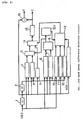
- FIG. 1 is a block diagram of a Y/C separation apparatus in accordance with a first exemplary embodiment of the present invention.
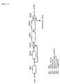
- FIG. 2 is a block diagram of a high band level detection circuit of a Y/C separation apparatus in accordance with the first exemplary embodiment of the present invention.
- FIG. 3 is a block diagram of a Y/C separation apparatus in accordance with a second exemplary embodiment of the present invention.
- FIG. 4 is a block diagram of a Y/C separation apparatus in accordance with a third exemplary embodiment of the present invention.
- FIG. 5 is a block diagram of a low band level difference detection circuit of a Y/C separation apparatus in accordance with the third exemplary embodiment of the present invention.
- FIG. 6 is a block diagram of a Y/C separation apparatus in accordance with the prior art.
- a Y/C separation apparatus in accordance with a first exemplary embodiment is explained below, referring to FIG. 1.
- FIG. 1 is a block diagram of a Y/C separation apparatus in accordance with a first exemplary embodiment of the present invention and FIG. 2 is a block diagram of a high band level detection circuit used in the Y/C separation apparatus.
- the block 1 is a first delay device for delaying an inputted composite color television signal by 1H.
- the block 2 is a second delay device for delaying the output of delay device 1 by 1H.
- the block 3 is a first comb filter for extracting a chrominance signal from the input signal and the output of delay device 1.
- the block 4 is a second comb filter for extracting a chrominance signal from the outputs of delay devices 1 and 2.
- the block 5 is a first BPF for extracting a chrominance signal from the outputs of delay device 1.
- the block 6 is a first correlation detection circuit for obtaining a correlation between the input signal and the output of delay device 1.
- the block 7 is a second correlation detection circuit for obtaining a correlation between the outputs of delay devices 1 and 2.
- the block 8 is a correlation judge circuit for obtaining a mixing ratio of the outputs of the comb filters according to the outputs of correlation detection circuits 6 and 7.
- the block 9 is a first mixer for mixing the outputs of comb filters 3 and 4 according to the output of correlation judge circuit 8.
- the block 10 is a first high band level detection circuit for extracting a subcarrier frequency component from the input signal.
- the block 11 is a second high band level detection circuit for extracting a subcarrier frequency component from the output of first delay device 1.
- the block 12 is a third high band level detection circuit for extracting a subcarrier frequency component from the output of second delay device 2.
- the block 13 is a BPF adaptation judge circuit for obtaining a mixing ratio of the output of first mixer 9 to the output of first BPF 5 according to the outputs of high band level detection circuits 10, 11 and 12.
- the block 14 is a second mixer for mixing the output of first mixer 9 and the output of first BPF 5 according to the output of BPF adaptation judge circuit 13.
- the block 15 is a second BPF for limiting the bandwidth of the output of mixer 14.
- the block 16 is a subtracter for subtracting the output of second BPF 15 from the output of first delay device 1.
- the block 201 is a third BPF for extracting a subcarrier frequency component from each input signal.
- the block 202 is an absolute value circuit for obtaining an absolute value of the output of BPF 201.
- the block 203 is a filter circuit for filtering the output of absolute value circuit 202.
- the block 204 is a comparator for comparing the output of filter circuit 203 with a designated threshold value.
- the inputted composite signal is delayed by each 1H at delay devices 1 and 2.
- the output of delay device 1 is a reference signal.
- Comb filters 3 and 4 are composed by making differences between the reference signal and the signals apart from the reference signal by 1H, ahead and behind.
- the comb filters separate chrominance signal components by subtracting the signals apart from the reference signal by 1H from the reference signal.
- a chrominance signal component is separated by making the reference signal as it is pass through first BPF 5.
- Correlation detection circuits 6 and 7 detect correlations between the reference signal and the signals apart from the reference signal by 1H, ahead and behind. Correlation is detected, for example, by filtering the absolute value of the difference between chrominance signal components of two signals and comparing the filtered output with a designated value.
- Correlation judge circuit 8 calculates a mixing ratio of the outputs of comb filters 3 and 4 according to the outputs of correlation detection circuits 6 and 7.
- Mixer 9 mixes the outputs of comb filters 3 and 4 corresponding to the calculated mixing ratio and outputs the mixed signal. Then, high band level detection circuits 10, 11 and 12 detect subcarrier frequency components from each signal on each line. If a subcarrier frequency component is not detected, it means that there is neither chrominance signal nor a high frequency component of a luminance signal.
- High band level detection circuit detects if the high band (subcarrier frequency component) level is under a designated threshold value, for example over one period of the subcarrier signal.
- a designated threshold value for example over one period of the subcarrier signal.
- the reference signal is a black signal not having a chrominance signal component and the signals on the other lines forming comb filters have a chrominance signal
- a chrominance signal component with a 1/2 level of a chrominance signal on the other line forming a comb filter is left in the signal passed the comb filter and passes subtracter 16 and dot interference appears on the luminance signal which is the reference signal.
- BPF adaptation judge circuit 13 In the case in which the reference signal is especially a black signal, dot interference is conspicuous comparing with the case in which the reference signal is not a black signal. What solves this problem is BPF adaptation judge circuit 13 and when the reference signal is in a black level, BPF adaptation judge circuit 13 judges to select the output of BPF 5.
- BPF adaptation judge circuit 13 filters the detected high band level, for example over one period of subcarrier and calculates a mixing ratio of the outputs of the BPFs. By this way, a smooth filter selection is possible.
- the output of first mixer 9 and the output of first BPF 5 are mixed at second mixer 14 according to the mixing ratio outputted from BPF adaptation judge circuit 13. When the reference signal is in a black level, BPF adaptation judge circuit 13 judges to select the output of first BPF 5.
- BPF adaptation judge circuit 13 similarly judges to select the output of first BPF 5.
- a chrominance signal is outputted from second BPF 15 by limiting the bandwidth of the output of second mixer 14 at second BPF 15.
- a luminance signal is outputted from subtracter 15 by subtracting the chrominance signal outputted from second BPF 15 from a time compensated signal by delaying by 1H from the apparatus input signal.
- FIG. 3 is a block diagram of a Y/C separation apparatus in accordance with a second exemplary embodiment of the present invention.
- a Y/C separation apparatus in accordance with a second exemplary embodiment is the same as that of the first exemplary embodiment except that a control circuit is added.
- the explanation of the blocks except the control circuit and their functions are omitted.
- the block 301 is a control circuit for controlling BPF adaptation judge circuit 13 forcibly not to adapt first BPF 5 when a vertical correlation exists.
- first BPF 5 is calculated by detecting the high band detection level of the reference signal and the signals apart by 1H from the reference signal (vertically near points to the reference signal position) in the first exemplary embodiment
- the second exemplary embodiment when vertical correlation is strong, it is controlled not to select first BPF 5.
- the output of first BPF 5 is not selected by mistake even for dark vertical lines and the like and a luminance resolution can be improved.
- FIG. 5 is a block diagram of a Y/C separation apparatus in accordance with a fourth exemplary embodiment of the present invention and FIG. 5 is a block diagram of a low band level difference detection circuit used in the Y/C separation apparatus.
- the configuration and the blocks of a Y/C separation apparatus in accordance with a third exemplary embodiment is the same as that of the second exemplary embodiment except a low band level difference detection circuit is added.
- the explanation of the blocks except the low band level difference detection circuit and their functions are omitted.
- the block 401 is a low band level difference detection circuit for detecting a low band level difference of the reference signal in a horizontal direction.
- the block 501 is a low pass filter (LPF) for extracting a low band component of the input signal.
- the block 502 is a delay device for delaying the output of LPF 501 in horizontal direction.
- the block 503 is a subtracter for detecting a difference between the input and the output of delay device 502.
- the block 504 is an absolute value circuit for obtaining an absolute value of the output of subtracter 503.
- the block 505 is a filter circuit for filtering the output of absolute value circuit 504.
- the block 506 is a comparator for comparing the output of filter circuit 505 with a designated threshold.' The output of filter circuit 505 is called horizontal correlation.
- a horizontal correlation of the low band component of the reference signal is detected and when there is no correlation, BPF adaptation judge circuit 13 is controlled so as to select the output of first mixer 9 without forcibly selecting the output of first BPF 5.
- BPF adaptation judge circuit 13 is controlled so as to select the output of first mixer 9 without forcibly selecting the output of first BPF 5.
- a Y/C separation apparatus of the present invention in an adaptive type Y/C separation separating a composite color television signal into a luminance signal and a chrominance signal, a Y/C separation which dot interference is not conspicuous even if correlation is detected by mistake is possible by detecting a high band level of the input signal and selecting a horizontal BPF when the high band level is low.
Landscapes
- Engineering & Computer Science (AREA)
- Multimedia (AREA)
- Signal Processing (AREA)
- Processing Of Color Television Signals (AREA)
Applications Claiming Priority (3)
| Application Number | Priority Date | Filing Date | Title |
|---|---|---|---|
| JP30305/96 | 1996-02-19 | ||
| JP3030596 | 1996-02-19 | ||
| JP8030305A JPH09224260A (ja) | 1996-02-19 | 1996-02-19 | Y/c分離装置 |
Publications (3)
| Publication Number | Publication Date |
|---|---|
| EP0790745A2 true EP0790745A2 (fr) | 1997-08-20 |
| EP0790745A3 EP0790745A3 (fr) | 1997-09-17 |
| EP0790745B1 EP0790745B1 (fr) | 2002-07-10 |
Family
ID=12300056
Family Applications (1)
| Application Number | Title | Priority Date | Filing Date |
|---|---|---|---|
| EP97300857A Expired - Lifetime EP0790745B1 (fr) | 1996-02-19 | 1997-02-11 | Appareil de séparation Y/C |
Country Status (7)
| Country | Link |
|---|---|
| US (1) | US5909255A (fr) |
| EP (1) | EP0790745B1 (fr) |
| JP (1) | JPH09224260A (fr) |
| KR (1) | KR100340358B1 (fr) |
| CN (1) | CN1120634C (fr) |
| AU (1) | AU719115B2 (fr) |
| DE (1) | DE69713822T2 (fr) |
Cited By (1)
| Publication number | Priority date | Publication date | Assignee | Title |
|---|---|---|---|---|
| EP1311127A3 (fr) * | 2001-11-13 | 2006-03-22 | Broadcom Corporation | Méthode et système pour la réduction de la diaphotie de luminance pour décodeurs de télévision multistandard |
Families Citing this family (30)
| Publication number | Priority date | Publication date | Assignee | Title |
|---|---|---|---|---|
| US6384873B1 (en) | 1999-12-03 | 2002-05-07 | Thomson Licensing S.A. | Vector magnitude control of a comb filter |
| KR100385958B1 (ko) * | 2001-03-12 | 2003-06-02 | 삼성전자주식회사 | Ntsc 복합 비디오 신호에 대한 휘도 및 색신호 분리장치 |
| US6738097B2 (en) * | 2001-04-11 | 2004-05-18 | Oki Electric Industry Co, Ltd. | Composite video signal decoder having stripe component judging section |
| CN1297152C (zh) * | 2002-12-06 | 2007-01-24 | 松下电器产业株式会社 | 图像信号处理装置及图像信号处理方法 |
| TW589905B (en) * | 2002-12-09 | 2004-06-01 | Vxis Technology Corp | Y/C separation circuit for processing TV signals |
| US7688387B2 (en) * | 2003-08-15 | 2010-03-30 | Broadcom Corporation | 2-D combing in a video decoder |
| US7489362B2 (en) | 2003-03-04 | 2009-02-10 | Broadcom Corporation | Television functionality on a chip |
| TWI222836B (en) * | 2003-03-21 | 2004-10-21 | Mediatek Inc | Video signal separating method and related apparatus |
| US7304688B1 (en) | 2003-05-20 | 2007-12-04 | Pixelworks, Inc. | Adaptive Y/C separator |
| US7605867B1 (en) | 2003-05-20 | 2009-10-20 | Pixelworks, Inc. | Method and apparatus for correction of time base errors |
| US7701512B1 (en) | 2003-05-20 | 2010-04-20 | Pixelworks, Inc. | System and method for improved horizontal and vertical sync pulse detection and processing |
| US7420625B1 (en) | 2003-05-20 | 2008-09-02 | Pixelworks, Inc. | Fuzzy logic based adaptive Y/C separation system and method |
| US7532254B1 (en) | 2003-05-20 | 2009-05-12 | Pixelworks, Inc. | Comb filter system and method |
| US7365796B1 (en) | 2003-05-20 | 2008-04-29 | Pixelworks, Inc. | System and method for video signal decoding using digital signal processing |
| KR20060021391A (ko) * | 2003-06-20 | 2006-03-07 | 코닌클리케 필립스 일렉트로닉스 엔.브이. | 휘도 및 컬러 분리 |
| TWI228935B (en) * | 2003-12-22 | 2005-03-01 | Sunplus Technology Co Ltd | Method of motion detection for 3D comb filter video decoder |
| TWI227630B (en) * | 2003-12-22 | 2005-02-01 | Sunplus Technology Co Ltd | A method of inter-frame Y/C separation |
| TWI248767B (en) * | 2004-11-19 | 2006-02-01 | Realtek Semiconductor Corp | Method and apparatus for Y/C separation |
| TWI253849B (en) * | 2004-12-14 | 2006-04-21 | Vxis Technology Corp | Brightness and chrominance separation circuit for three-dimensional image signal |
| KR100674939B1 (ko) * | 2005-01-13 | 2007-01-26 | 삼성전자주식회사 | 프레임 기반의 적응적 시공간 y/c 분리를 위한 디지털영상 신호 처리 장치 및 방법 |
| KR100674940B1 (ko) * | 2005-01-13 | 2007-01-26 | 삼성전자주식회사 | 적응적 시공간 다방향 y/c분리를 위한 디지털 영상 신호처리 장치 및 방법 |
| KR100688519B1 (ko) * | 2005-01-13 | 2007-03-02 | 삼성전자주식회사 | 필드 기반의 적응적 시공간 y/c 분리를 위한 디지털영상 신호 처리 장치 및 방법 |
| US7345710B2 (en) * | 2005-02-07 | 2008-03-18 | Mediatek Inc. | Systems and methods for processing composite television signals |
| KR20070012047A (ko) * | 2005-07-22 | 2007-01-25 | 삼성전자주식회사 | 디지털 영상처리장치 및 그 제어방법 |
| JP4843367B2 (ja) * | 2006-04-28 | 2011-12-21 | 株式会社東芝 | Y/c分離回路 |
| TWI338516B (en) * | 2006-09-21 | 2011-03-01 | Realtek Semiconductor Corp | Video processing system and related video processing method |
| JP2008098917A (ja) * | 2006-10-11 | 2008-04-24 | Denso Corp | 信号分離装置 |
| JP4935288B2 (ja) | 2006-10-11 | 2012-05-23 | 株式会社デンソー | 信号分離装置 |
| TWI372554B (en) * | 2007-07-26 | 2012-09-11 | Realtek Semiconductor Corp | Motion detecting method |
| CN101500174B (zh) * | 2008-01-29 | 2010-12-01 | 瑞昱半导体股份有限公司 | 动态选择亮度/色度分离的方法与相关装置 |
Family Cites Families (19)
| Publication number | Priority date | Publication date | Assignee | Title |
|---|---|---|---|---|
| US4050084A (en) * | 1976-07-14 | 1977-09-20 | Cbs Inc. | Comb filter for television signals having adaptive features |
| GB8509306D0 (en) * | 1985-04-11 | 1985-05-15 | British Broadcasting Corp | Pal decoders |
| JPH0720265B2 (ja) * | 1988-11-04 | 1995-03-06 | 三菱電機株式会社 | 映像信号処理回路 |
| JPH0720256B2 (ja) * | 1989-06-26 | 1995-03-06 | 三洋電機株式会社 | 輝度信号分離回路 |
| JPH0366287A (ja) * | 1989-08-04 | 1991-03-20 | Matsushita Electric Ind Co Ltd | 信号分離装置 |
| KR930005626Y1 (ko) * | 1991-02-28 | 1993-08-27 | 김영선 | 탁자다리 결착장치 |
| KR940000409Y1 (ko) * | 1991-04-13 | 1994-01-24 | 삼성전자 주식회사 | 자동 샤프니스 조절 회로 |
| KR940001442B1 (ko) * | 1991-07-26 | 1994-02-23 | 주식회사 금성사 | 휘도신호 및 색신호 분리 시스템 |
| KR940004559B1 (ko) * | 1991-11-26 | 1994-05-25 | 주식회사 금성사 | 정방형 변조된 칼라 텔레비젼 수상기의 스펙트럼 분포 적응형 휘도/칼라신호 분리장치 |
| JP3263791B2 (ja) * | 1992-09-30 | 2002-03-11 | ソニー株式会社 | Yc分離回路 |
| KR0123768B1 (ko) * | 1992-10-20 | 1997-11-26 | 윤종용 | 적응형이차원휘도/색신호분리방법및장치 |
| EP0613311A1 (fr) * | 1993-02-26 | 1994-08-31 | Kabushiki Kaisha Toshiba | Circuit de séparation Y/C |
| US5347321A (en) * | 1993-09-30 | 1994-09-13 | Texas Instruments Incorporated | Color separator for digital television |
| JP3216365B2 (ja) * | 1993-10-21 | 2001-10-09 | 松下電器産業株式会社 | Y/c分離装置 |
| JP3216364B2 (ja) * | 1993-10-21 | 2001-10-09 | 松下電器産業株式会社 | Y/c分離装置 |
| JP3227941B2 (ja) * | 1993-10-22 | 2001-11-12 | 松下電器産業株式会社 | 色度信号分離装置 |
| JP3163886B2 (ja) * | 1994-03-02 | 2001-05-08 | 松下電器産業株式会社 | 輪郭補正装置 |
| JP3149677B2 (ja) * | 1994-04-21 | 2001-03-26 | 松下電器産業株式会社 | Y/c分離装置 |
| JP3480477B2 (ja) * | 1995-07-26 | 2003-12-22 | ソニー株式会社 | 動き検出回路および動き検出方法、並びに輝度・色信号分離装置 |
-
1996
- 1996-02-19 JP JP8030305A patent/JPH09224260A/ja active Pending
-
1997
- 1997-02-11 EP EP97300857A patent/EP0790745B1/fr not_active Expired - Lifetime
- 1997-02-11 DE DE69713822T patent/DE69713822T2/de not_active Expired - Fee Related
- 1997-02-12 AU AU12642/97A patent/AU719115B2/en not_active Ceased
- 1997-02-18 KR KR1019970004894A patent/KR100340358B1/ko not_active Expired - Fee Related
- 1997-02-18 US US08/801,191 patent/US5909255A/en not_active Expired - Fee Related
- 1997-02-19 CN CN97102537A patent/CN1120634C/zh not_active Expired - Fee Related
Cited By (1)
| Publication number | Priority date | Publication date | Assignee | Title |
|---|---|---|---|---|
| EP1311127A3 (fr) * | 2001-11-13 | 2006-03-22 | Broadcom Corporation | Méthode et système pour la réduction de la diaphotie de luminance pour décodeurs de télévision multistandard |
Also Published As
| Publication number | Publication date |
|---|---|
| JPH09224260A (ja) | 1997-08-26 |
| CN1120634C (zh) | 2003-09-03 |
| EP0790745B1 (fr) | 2002-07-10 |
| KR970064280A (ko) | 1997-09-12 |
| AU719115B2 (en) | 2000-05-04 |
| CN1162894A (zh) | 1997-10-22 |
| US5909255A (en) | 1999-06-01 |
| KR100340358B1 (ko) | 2002-11-22 |
| EP0790745A3 (fr) | 1997-09-17 |
| DE69713822T2 (de) | 2002-11-14 |
| DE69713822D1 (de) | 2002-08-14 |
| AU1264297A (en) | 1997-08-28 |
Similar Documents
| Publication | Publication Date | Title |
|---|---|---|
| US5909255A (en) | Y/C separation apparatus | |
| US5325186A (en) | Motion adaptive luminance signal and color signal separating filter | |
| US5311306A (en) | Motion detecting circuit for video signal processor | |
| US5155582A (en) | Dot crawling interference elimination device and color subcarrier vertical correlation detection device | |
| US5500686A (en) | Motion adaptive luminance signal/chrominance signal separation filter | |
| EP1207701B1 (fr) | Circuit de séparation d'un signal de luminance et d'un signal de chrominance | |
| US5225899A (en) | Correlation adaptive luminance and chrominance signal separating circuit | |
| EP0590831A2 (fr) | Circuits de séparation des signaux luminance/chrominance | |
| US6738097B2 (en) | Composite video signal decoder having stripe component judging section | |
| KR940000414Y1 (ko) | 화상신호의 휘도 신호 및 색신호 분리장치 | |
| US5508753A (en) | Luminance and chrominance signal separating apparatus | |
| US5500687A (en) | Chrominance signal separator using chrominance signal correlation | |
| US8218084B2 (en) | Signal separator | |
| KR19980079061A (ko) | 휘도 및 색 신호 분리 방법 및 이를 수행하기 위한 휘도 및 색 신호 분리 회로 | |
| US20080088745A1 (en) | Signal separator | |
| JP2529683B2 (ja) | 画像相関対応輝度信号色信号分離フイルタ | |
| JPH099169A (ja) | テレビジョン受像機 | |
| JP3503442B2 (ja) | 2ラインyc分離装置 | |
| JPH1066102A (ja) | Y/c分離回路 | |
| JPH0530530A (ja) | 動き適応輝度信号・色信号分離回路 | |
| JP2624700B2 (ja) | カラー映像信号処理装置 | |
| JPH06292228A (ja) | 輝度信号・色信号分離回路 | |
| JP2596738B2 (ja) | 画像相関対応輝度信号色信号分離フイルタ | |
| JP2596736B2 (ja) | 画像相関対応輝度信号色信号分離フイルタ | |
| JPH04351090A (ja) | Y/c分離装置 |
Legal Events
| Date | Code | Title | Description |
|---|---|---|---|
| PUAI | Public reference made under article 153(3) epc to a published international application that has entered the european phase |
Free format text: ORIGINAL CODE: 0009012 |
|
| PUAL | Search report despatched |
Free format text: ORIGINAL CODE: 0009013 |
|
| AK | Designated contracting states |
Kind code of ref document: A2 Designated state(s): DE GB NL |
|
| AK | Designated contracting states |
Kind code of ref document: A3 Designated state(s): DE GB NL |
|
| K1C3 | Correction of patent application (complete document) published |
Effective date: 19970820 |
|
| 17P | Request for examination filed |
Effective date: 19971017 |
|
| 17Q | First examination report despatched |
Effective date: 19991004 |
|
| GRAG | Despatch of communication of intention to grant |
Free format text: ORIGINAL CODE: EPIDOS AGRA |
|
| GRAG | Despatch of communication of intention to grant |
Free format text: ORIGINAL CODE: EPIDOS AGRA |
|
| GRAH | Despatch of communication of intention to grant a patent |
Free format text: ORIGINAL CODE: EPIDOS IGRA |
|
| GRAH | Despatch of communication of intention to grant a patent |
Free format text: ORIGINAL CODE: EPIDOS IGRA |
|
| GRAA | (expected) grant |
Free format text: ORIGINAL CODE: 0009210 |
|
| AK | Designated contracting states |
Kind code of ref document: B1 Designated state(s): DE GB NL |
|
| REG | Reference to a national code |
Ref country code: GB Ref legal event code: FG4D |
|
| REF | Corresponds to: |
Ref document number: 69713822 Country of ref document: DE Date of ref document: 20020814 |
|
| PLBE | No opposition filed within time limit |
Free format text: ORIGINAL CODE: 0009261 |
|
| STAA | Information on the status of an ep patent application or granted ep patent |
Free format text: STATUS: NO OPPOSITION FILED WITHIN TIME LIMIT |
|
| 26N | No opposition filed |
Effective date: 20030411 |
|
| PGFP | Annual fee paid to national office [announced via postgrant information from national office to epo] |
Ref country code: NL Payment date: 20070204 Year of fee payment: 11 |
|
| PGFP | Annual fee paid to national office [announced via postgrant information from national office to epo] |
Ref country code: GB Payment date: 20070207 Year of fee payment: 11 |
|
| PGFP | Annual fee paid to national office [announced via postgrant information from national office to epo] |
Ref country code: DE Payment date: 20070208 Year of fee payment: 11 |
|
| GBPC | Gb: european patent ceased through non-payment of renewal fee |
Effective date: 20080211 |
|
| NLV4 | Nl: lapsed or anulled due to non-payment of the annual fee |
Effective date: 20080901 |
|
| PG25 | Lapsed in a contracting state [announced via postgrant information from national office to epo] |
Ref country code: NL Free format text: LAPSE BECAUSE OF NON-PAYMENT OF DUE FEES Effective date: 20080901 |
|
| PG25 | Lapsed in a contracting state [announced via postgrant information from national office to epo] |
Ref country code: DE Free format text: LAPSE BECAUSE OF NON-PAYMENT OF DUE FEES Effective date: 20080902 |
|
| PG25 | Lapsed in a contracting state [announced via postgrant information from national office to epo] |
Ref country code: GB Free format text: LAPSE BECAUSE OF NON-PAYMENT OF DUE FEES Effective date: 20080211 |