EP0791935A2 - Nichtflüchtige Halbleiterspeicher - Google Patents
Nichtflüchtige Halbleiterspeicher Download PDFInfo
- Publication number
- EP0791935A2 EP0791935A2 EP96309474A EP96309474A EP0791935A2 EP 0791935 A2 EP0791935 A2 EP 0791935A2 EP 96309474 A EP96309474 A EP 96309474A EP 96309474 A EP96309474 A EP 96309474A EP 0791935 A2 EP0791935 A2 EP 0791935A2
- Authority
- EP
- European Patent Office
- Prior art keywords
- main bit
- bit lines
- bit line
- group
- mbi
- Prior art date
- Legal status (The legal status is an assumption and is not a legal conclusion. Google has not performed a legal analysis and makes no representation as to the accuracy of the status listed.)
- Withdrawn
Links
Images





Classifications
-
- G—PHYSICS
- G11—INFORMATION STORAGE
- G11C—STATIC STORES
- G11C17/00—Read-only memories programmable only once; Semi-permanent stores, e.g. manually-replaceable information cards
-
- G—PHYSICS
- G11—INFORMATION STORAGE
- G11C—STATIC STORES
- G11C17/00—Read-only memories programmable only once; Semi-permanent stores, e.g. manually-replaceable information cards
- G11C17/08—Read-only memories programmable only once; Semi-permanent stores, e.g. manually-replaceable information cards using semiconductor devices, e.g. bipolar elements
- G11C17/10—Read-only memories programmable only once; Semi-permanent stores, e.g. manually-replaceable information cards using semiconductor devices, e.g. bipolar elements in which contents are determined during manufacturing by a predetermined arrangement of coupling elements, e.g. mask-programmable ROM
- G11C17/12—Read-only memories programmable only once; Semi-permanent stores, e.g. manually-replaceable information cards using semiconductor devices, e.g. bipolar elements in which contents are determined during manufacturing by a predetermined arrangement of coupling elements, e.g. mask-programmable ROM using field-effect devices
- G11C17/126—Virtual ground arrays
-
- G—PHYSICS
- G11—INFORMATION STORAGE
- G11C—STATIC STORES
- G11C16/00—Erasable programmable read-only memories
- G11C16/02—Erasable programmable read-only memories electrically programmable
- G11C16/04—Erasable programmable read-only memories electrically programmable using variable threshold transistors, e.g. FAMOS
- G11C16/0491—Virtual ground arrays
Definitions
- the invention relates in general to nonvolatile semiconductor memory and more particularly to such a memory employing flat-typed memory cells.
- Read only memories generally referred to as nonvolatile memories
- the NOR-typed cell array has the advantage of obtaining efficient current drive ability while it has a shortage of increasing cell size.
- the flat-typed cell array is logically a kind of the NOR-typed arrangement.
- Nonvolatile memories having the flat-typed memory cell array have been disclosed in several articles, e.g., entitled "12-Mb ROM Design Using Bank Select Architecture” (88 SYMPOSIUM ON VLSI CIRCUITS, V1-7, pp.85-86).
- the architecture of the memory cell array of the article is shown in Fig. 1, wherein memory cell blocks are selected by means of activations of selection signals SOm (for odd columns) and SEm (for even columns) where SOm-1 and SEm+1 conduct for adjacent memory blocks.
- Bit lines are classified into main bit lines MBi-1 to MBi+2 and sub bit lines SB2i-3 to SB2i+4. Every two sub bit lines is subjected to one main bit line, and main bit lines MBi-1 and MBi+1 act as virtual ground lines.
- Sense amplifier connected to MBi through column gate transistor TY2, generates a data bit "1" or or "0" from detecting a voltage level on MBi which is determined by a threshold voltage of selected memory cell RC 13.
- MBi is pulled down and then sense amplifier SAx reads "0".
- the discharging current at this time flows, as shown with the broken line in FIG 1, through main bit line MBi, odd column selection transistor TO5, sub bit line SB2i-1, memory cell RCn2, odd column selection transistor TO3, main bit line MBi-1, column gate transistor TY1, ground selection transistor TG1 and Vss, in this order.
- a voltage drop, caused by conductive on-cells, is substantially made up throughout the resistance in diffusion regions by which the sub bit line is constructed.
- the amount of the current flowing through the on-cell e.g., RCn2
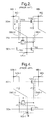
- Fig. 2 The case of the current where an information is read out from memory cell RCn2 is considered with Fig. 2, as follows. In this case, as shown in Fig. 2, the aforementioned current flowing meets resistance r2 of a partial diffusion region which connects odd column selection transistor TO5 to memory cell RCn2 and resistance r1 of a partial diffusion region which connects memory cell RCn2 to odd column selection transistor TO3.
- main bit line MBi While, assuming that when another read operation is conducting for memory cell RC12 with a threshold voltage larger than Vcc (VT>Vcc; hereinafter, such a memory cell mat be called to as "off-cell"), main bit line MBi must be pulled up to high level and thereby sense amplifier SAx must detect "1" from the main bit line MBi.
- the current from sense amplifier SAx flows into adjacent main bit lines (e.g., MBi+1, MBi+2,..) through the adjacent memory cells connected to W11 and odd column selection transistors responding to odd column selection signal SOm, while there is no current path towards the main bit line MBi-1 due to the nonconductive memory cell RC12.
- adjacent main bit lines e.g., MBi+1, MBi+2,..
- the unwanted current entrance into the adjacent bit lines makes it difficult for the main bit line MBi to retain high level, so that a read-out time for data bit "1" becomes longer in proportion as the current amount induced thereby.
- Fig. 3 figures out the architecture of memory cell array disclosed in the patented specification, being with same dimension of Fig. 1.
- memory blocks B2i-2 to B2i+2 are arranged in row direction, each block being numbered with odd and even therein, and sub bit lines SB2i-3 to SB2i+4 are interposed between the memory blocks.
- Each sub bit line is connected in common to memory cells of adjacent memory blocks, and main bit lines MBi-1 to MBi+2, arranged in parallel with the sub bit lines, are positioned at columns by two.
- main bit line MBi is connected to SB2i-3 through odd column selection transistor TOi-1 at node NOi-1, to SB2i-1 through TEi at node NEi-1 and directly to SB2i-2.
- Fig. 4 may prove more advanced configurations about the current drivability rather than in Fig. 2, in which the sensing current flows through two transistors and parasitic resistances.
- the circuit architecture as shown in Fig. 3 has at least bit line capacitance value of four times from that in Fig. 1, at a node (e.g., NOi) to where main bit line and sub bit line are coupled each other (note that main bit line of Fig. 1 is just connected to source and drain diffusion regions between cell transistors), because a main bit line is connected to a sub bit line coupled to source and drain diffusion regions between adjacent cell transistors, and further to such two sub bit lines.
- NOi node
- main bit line of Fig. 1 is just connected to source and drain diffusion regions between cell transistors
- One aspect is a semiconductor memory including a plurality of main bit lines led to sense amplifiers and arranged in a row direction, a first group of sub bit lines interposed between the memory banks and connected to the main bit lines through a first group of selection transistors, a second group of sub bit lines interposed between the memory banks and the first group of sub bit lines and connected to a common ground line through a second group of selection transistors.
- Another aspect is a semiconductor memory including a plurality of main bit lines led to sense amplifiers and arranged in a row direction, a plurality of sub bit lines interposed between said memory banks and connected to the main bit lines respectively through a first group of selection transistors and a second group of selection transistors, means for connecting a first group of the main bit lines to sense amplifiers and connecting other main bit lines adjacent to the first group of the main bit lines to a ground voltage.
- a semiconductor memory including a first group of main bit lines arranged in a row direction and connected to a ground voltage, a second group of main bit lines arranged in the row direction and connected to sense amplifiers, a first group of sub bit lines interposed between the memory banks and connected to the first and second groups of main bit lines respectively through a first group of selection transistors and a second group of selection transistors, a second group of sub bit lines interposed between the memory banks and the first group of sub bit lines, a first group of bank selection transistors whose gates are coupled to a first selection signal in common and whose channel paths are interposed between said first and second groups of sub bit lines, and a second group of bank selection transistors whose gates are coupled to a second selection signal in common and whose channel paths are interposed between said first and second groups of sub bit lines.
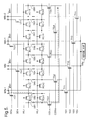
- main bit line MBi-1 to MBi+2 arranged in row direction with a pitch by two memory banks spacing, extends to column direction and coupled to sense amplifier SAx through column selection transistors TY1 to TY3 which are controlled by column gate signals YS1 to YS4.
- Each of word lines WL1 to WL3 is connected to gates of memory cells RC11 to RCn1, RC12 to RCn2,..and RC18 to RCn8 of each memory bank.
- Between memory banks extend sub bit lines SB1 ro SB9 in parallel with the main bit lines.
- the sub bit lines are coupled to sources and drains of memory cells belonging to adjacent memory banks, being divided two groups that one is connected to Vss and the other to a main bit line.
- sub bit line SB1 is connected to Vss through common ground line VGL and ground selection transistor TG1 whose gate is coupled to ground selection signal GSLm.
- Sub bit line SB2 is connected to main bit line MBi-1 at bit line node BN1 through odd column selection transistor TO1 whose gate is coupled to odd column selection signal SOm.
- Sub bit line SB3 is connected to Vss through common ground line VGL and ground selection transistor TG2 whose gate is coupled to ground selection signal GSLm.
- Sub bit line SB4 is connected to main bit line MBi at bit line node BN2 through even column selection transistor TE2 whose gate is coupled to even column selection signal SEm.
- Sub bit line SB5 is connected to Vss through common ground line VGL and ground selection transistor TG3 whose gate is coupled to ground selection signal GSLm.
- Sub bit line SB6 is connected to main bit line MBi+1 at bit line node BN3 through odd column selection transistor TO3 whose gate is coupled to odd column selection signal SOm.
- Sub bit line SB7 is connected to Vss through common ground line VGL and ground selection transistor TG4 whose gate is coupled to ground selection signal GSLm.
- Sub bit line SB8 is connected to main bit line MBi+2 at bit line node BN4 through even column selection transistor TE4 whose gate is coupled to even column selection signal SEm.
- Sub bit line SB9 is connected to Vss through common ground line VGL and ground selection transistor TG5 whose gate is coupled to ground selection signal GSLm.
- Ground selection transistors TG1 to TG5 are connected to common ground line VGL at nodes GN1 to GN5, respectively.
- a read operation in Fig. 5 will be as follows. Assuming that memory cell RC11 is selected, voltage level of Vcc (hereinafter referred to as “high voltage” or “high”) is applied to selected word line WL1 while a voltage level of Vss (hereinafter referred to as “low voltage” or “low”) is applied to other unselected word lines WL2 through WLn. Odd column selection transistors TO1 and TO3 become conductive in response to odd column selection signal SOm of high, and even column transistors TE2 and TE4 become non-conductive by even column selection signal SEm of low.
- column gate selection signal YS1 goes to high so as to activate corresponding main bit line (e.g., MBi-1), making column gate transistor TY1 which connects main bit line MBi-1 to sense amplifier SAx be turned on.
- Other column gate selection transistors TY2 to TY4 retain non-conductive states.
- ground selection transistor connecting sub bit line SB1 coupled to the source of memory cell RC11 to common ground line VGL, is turned on in response to ground selection signal GSLm.
- Another ground selection signal GSRm retains a disable voltage level of low. Therefore, the voltage level on main bit line MBi-1 goes to high or low according to whether a data bit from selected memory cell RC11 is "1" or "0", and then sense amplifier SAx reads the current voltage level on the main bit line.
- the selected memory cell RC11 is an off-cell (VT>Vcc)
- the voltage level on main bit line MBi-1 rises to high and data bit "1" is read out from sense amplifier SAx. While this, as mentioned in Fig. 1, since a current path cannot be formed towards adjacent main bit line MBi because adjacent ground selection transistor TG2 and even column selection transistor TE2 are being turned off, even though other memory cell RC12 to RC18 coupled to the selected word line WL1 are all on-cells, current flowing into sense amplifier SAx is not induced to adjacent main bit lines MBi and MBi-2. Thus, the current from sense amplifier SAx is almost consumed in charging the selected main bit line MBi-1 and thereby the main bit line MBi-1 is satisfactorily held on high level.
- main bit line MBi-1 is pulled down to low and then data bit "0" is read out from sense amplifier SAx.
- Resistance components throughout the current discharging path consists of resistance in source and drain diffusion regions and further capacitance on bit lines is reduced by a half (of that in the case of Fig. 1 in which the discharging path includes two main bit lines), resulting in shortage of read-out time for data bit "0".
- main bit line MBi-2 are arranged in row direction, each other being spaced with a pitch by two mwmory banks, Between memory banks, sub bit lines SB 1 to SB9 are positioned in parallel with the main bit lines MBi-2 to MBi+1. Each of the main bit lines is connected to two sub bit lines through odd column selection transistors TO1 to TO9 and even column selection transistors TE1 to TE9.
- sub bit line SB1 is connected to main bit line MBi-2 repectively through odd column selection transistor TO1 and even column selection transistor TE1.
- Sub bit line SB2 is connected to main bit line MBi-1 repectively through odd column selection transistor TO2 and even column selection transistor TE2, and sub bit line SB3 to main bit line MBi-1 repectively through odd column selection transistor TO3 and even column selection transistor TE3.
- Sub bit line SB4 is connected to main bit line MBi-1 repectively through odd column selection transistor TO4 and even column selection transistor TE4, main bit line MBi. also being connected to sub bit line SB5 respectively through odd column selection transistor TO5 and even column selection transistor TE5.
- Sub bit line SB6 is connected to main bit line MBi+1 repectively through odd column selection transistor TO6 and even column selection transistor TE6, main bit line MBi+1 also being connected to sub bit line SB7 respectively through odd and even column selection transistor TO7 and TE7.
- Sub bit line SB8 is connected to main bit line MBi+2 repectively through odd and even column selection transistor TO8 and TE8 and main bit line MBi+2 is also connected to sub bit line SB9 respectively through odd and even column selection transistor TO9 and TE9.
- Gate electrodes of odd column selection transistors TO1 to TO9 are coupled to odd column selection signal SOm in common, and gate electrodes of even column selection transistors TE1 to TE9 all receives even column selection signal SEm.
- the array structure described above is repeatedly arranged over the entire memory cell array.
- Main bit line MBi-2 is connected to Vss through ground connection transistor TNG1 whose gate is coupled to Vcc to be in a normal-conductive state.
- Main bit line MBi-1 is connected to Vss through ground selection transistor TG1 whose gate is coupled to column selection line YAi1, and is led to sense amplifier SAx both through column selection transistor TY1 whose gate is coupled to column selection line YAi0 and through column selection transistor TY5 whose gate is coupled to column selection line YBi0.
- Main bit line MBi is led to sense amplifier SAy both through column selection transistors TY2 and TY3 in parallel connection whose gates are coupled to column selection lines YAi0 and YAi1, repectively, and through column selection transistor TY6 whose gate is coupled to column selection line YBi0.
- Main bit line MBi+1 is connected to Vss through ground selection transistor TG2 whose gate is coupled to column selection line YAi0, and is led to sense amplifier SAx both through column selection transistor TY4 whose gate is coupled to column selection line YAi1 and through column selection transistor TY5 whose gate is coupled to column selection line YBi0.
- Main bit line MBi+2 is connected to Vss through ground connection transistor TNG2 whose gate is coupled to Vcc so as to be in a normal-conductive state.
- Main bit line MBi acts as a virtual bit line through which a voltage level responding to charges stored in the delected memory cell is transferred into sense amplifier SAy, and main bit lines MBi-2 and MBi+2 is conducted to as virtual ground lines with being connected to Vss.
- Main bit lines MBi-1 and MBi+1 adjacent to main bit line MBi are determined to be coducted to as the virtual bit lines or the virtual ground lines in accordance with what present voltage levels on column selection lines YAi0, YAi1 and YBi0 is.
- the voltage levels on the column selection lines follow coding configurations with combinations of address signals supplied from external lines,each being pulled up to high or pulled down to low.
- sense amplifier SAx makes it a rule to use main bit lines MBi-1 and MBi-2 as the virtual bit line and the virtual ground line, respectively, when a read operation is being conducted to memory cells RC11 through RCn1 and RC12 through RCn2, or main bit line MBi+1 acts as the virtual bit line while main bitline MBi+2 as the virtual ground line when a read operation is being conducted to memory cells RC17 through RCn7 and RC18 through RCn8.
- sense amplifier SA reads main bit line MBi into the virtual bit line and uses MBi-1 or MBi+1 for the virtual ground line.
- main bit line MBi+1 acts as the virtual ground line against the selected main bit line MBi.
- Main bit line MBi+2 fixed into Vss is used for the virtual groups line for main bit line MBi-1.
- main bit lines MBi-2 and MBi+1 adjacent to main bit lines MBi-1 and MBi whch act as the virtual bit lines are used for the virtual ground lines and thereby there are no forming of unwnated current paths over the cell array of Fig. 6 as is Fig. 1.
- main bit lines MBi-1 to MBi+2 being arranged in row direction with a pitch by two memory banks, extend to column direction and are alternately connected to ground votages and sense amplifiers. Namely, main bit lines MBi-1 and MBi+1 are connected to Vss so as to be the virtual ground lines, and main bit lines MBi and MBi+2 are led to sense amplifiers SAx and SAy, respectively, as the virtual bit lines.
- Gate electrodes of memory cells RC11 to RCn1, RC12 to RCn2,..and RC18 to RCn8 are connected to word lines WL1 to WLn, respectively.
- Sub bit lines SB1 to SB8 extend in parallel with the main bit lines, between memory banks. Each of the sub bit lines is connected to sources and drains of memory cells belonging to adjacent memory banks and also connected to sources and drains of bank selection transistors introduced hereinbelow.
- Sub bit lines SB1 to SB8 positioned between memory banks are said to be distinguished into two groups; one, of SB1, SB3, Sb5 and SB7, is to be connected to main bit lines through block selection transistors, and the other is not, like SB2, SB4 and SB6. It should be noted that, in this embodiment, two memory banks construct one memory bank.
- Sub bit line SB1 is connected to main bit line MBi-1 at the upper and bottom sides of the memory array through block selection transistors TB1 and TB5.
- Sub bit line SB3 is connected to main bit line MBi at the upper and bottom sides of the memory array through block selection transistors TB2 and TB6.
- Sub bit line SB5 is connected to main bit line MBi+1 at the upper and bottom sides of the memory array through block selection transistors TB3 and TB7.
- Sub bit line SB7 is connected to main bit line MBi+2 at the upper and bottom sides of the memory array through block selection transistors TB4 and TB8.
- Gate electrodes of block selection transistors TB1 to TB8 are coupled to block selection signal BLSm in common.
- bank selection transistors TR1 to TR4 and TL1 to TL3 are arranged over the center portion of the memory banks so as to select memory banks which are located left and light from a main bit line.
- bank selection transistor TR1 is interposed between sub bit lines SB1 and SB2, bank selection transistor TL1 between sub bit lines SB2 and SB3, bank selection transistor TR2 between sub bit lines SB3 and SB4, bank selection transistor TL2 between sub bit lines SB4 and SB5, bank selection transistor TR3 between sub bit lines SB5 and SB6, bank selection transistor TL3 between sub bit lines SB6 and SB7 and bank selection transistor TR4 between sub bit lines SB7 and SB8.
- Gate electrodes of the bank selection transistors TR1 to TR4 which belong to the memory banks positioned at the right sides of the main bit lines respectively are coupled to bank selection signal SSRm in common, while bank selection signal SSLm is applied to all gate electrodes of bank selection transistors TL1 to TL3 which belong to the memory banks positioned at the left sides of the main bit lines respectively.
- the structure of the memory cell array of Fig. 7 is a portion of an entire memory cell array according to the present embodiment.
- bank selection signal SSRm is pulled up to high so as to activate bank selection transistor TR1 and bank selection signal SSLm is pulled down to low so as to cut bank selection transistor TL1.
- the read current flows through main bit line MBi, block selection transistor TB2, sub bit line SB3, memory cell RCn2, sub bit line SB2, bank selection transistor TR1, sub bit line SB1, block selection transistor TB5, main bit line MBi-1 and Vss, in this order. While this, the voltage level in main bit line MBi is held on low and thereby data bit "0" is read out fron sense amplifier SAx. During this read-out operation, resistance throughout the current path is only composed of components by one memory block, as is in Fig. 5, being lower than that of Fig. 1 by a half.
- main bit line MBi retains high and sense amplifier SAx reads data bit "1" therefrom.
- leakage current (or unwanted discharging current flow) among the memory banks can be reduced by non-conductive bank sekection transistors TL1 to TL3.
- the invention has an advantage of reducing leakage current flowing between mamory banks and degradation of read-out current, resulting in high speed read operation. Furthermore, parasitic capacitances on bit lines can be reduced by decrease of the unwanted current consumption, so that it is possible to enhance an operational reliability of a nonvolatile memory such as a read only memory.
Landscapes
- Engineering & Computer Science (AREA)
- Microelectronics & Electronic Packaging (AREA)
- Read Only Memory (AREA)
- Non-Volatile Memory (AREA)
- Semiconductor Memories (AREA)
- Static Random-Access Memory (AREA)
Applications Claiming Priority (2)
| Application Number | Priority Date | Filing Date | Title |
|---|---|---|---|
| KR1019950067815A KR0172378B1 (ko) | 1995-12-30 | 1995-12-30 | 불휘발성 반도체 메모리소자 |
| KR9567815 | 1995-12-30 |
Publications (2)
| Publication Number | Publication Date |
|---|---|
| EP0791935A2 true EP0791935A2 (de) | 1997-08-27 |
| EP0791935A3 EP0791935A3 (de) | 1999-09-08 |
Family
ID=19447905
Family Applications (1)
| Application Number | Title | Priority Date | Filing Date |
|---|---|---|---|
| EP96309474A Withdrawn EP0791935A3 (de) | 1995-12-30 | 1996-12-24 | Nichtflüchtige Halbleiterspeicher |
Country Status (6)
| Country | Link |
|---|---|
| US (1) | US5909405A (de) |
| EP (1) | EP0791935A3 (de) |
| JP (1) | JP3814037B2 (de) |
| KR (1) | KR0172378B1 (de) |
| CN (1) | CN1125466C (de) |
| TW (1) | TW371345B (de) |
Families Citing this family (15)
| Publication number | Priority date | Publication date | Assignee | Title |
|---|---|---|---|---|
| JP3211745B2 (ja) * | 1997-09-18 | 2001-09-25 | 日本電気株式会社 | 半導体記憶装置 |
| US6033955A (en) * | 1998-09-23 | 2000-03-07 | Advanced Micro Devices, Inc. | Method of making flexibly partitioned metal line segments for a simultaneous operation flash memory device with a flexible bank partition architecture |
| JP3583042B2 (ja) * | 1999-11-09 | 2004-10-27 | Necエレクトロニクス株式会社 | 半導体記憶装置 |
| JP2001297593A (ja) * | 2000-04-10 | 2001-10-26 | Nec Corp | 半導体記憶装置及びデータ出力方法 |
| KR100725093B1 (ko) * | 2001-03-15 | 2007-06-04 | 삼성전자주식회사 | 노아 타입 플랫 셀을 가지는 반도체 메모리 장치 및 그의구동방법 |
| JP4633958B2 (ja) * | 2001-05-07 | 2011-02-16 | ルネサスエレクトロニクス株式会社 | 不揮発性半導体メモリ |
| US6480422B1 (en) * | 2001-06-14 | 2002-11-12 | Multi Level Memory Technology | Contactless flash memory with shared buried diffusion bit line architecture |
| JP3640179B2 (ja) * | 2001-07-23 | 2005-04-20 | セイコーエプソン株式会社 | 不揮発性半導体記憶装置 |
| US6870752B2 (en) * | 2001-08-16 | 2005-03-22 | Macronix International Co., Ltd. | High density mask ROM having flat-type bank select |
| US6563735B1 (en) * | 2002-04-04 | 2003-05-13 | Macronix International Co., Ltd. | NOR-structured semiconductor memory device |
| KR100492774B1 (ko) * | 2002-12-24 | 2005-06-07 | 주식회사 하이닉스반도체 | 라이트 보호 영역을 구비한 비휘발성 메모리 장치 |
| ITTO20030121A1 (it) * | 2003-02-18 | 2004-08-19 | St Microelectronics Srl | Amplificatore di lettura di celle di memoria non volatili a |
| WO2008148091A1 (en) * | 2007-05-25 | 2008-12-04 | Marvell World Trade Ltd. | Tree type bit line decoder architecture for nor-type memory array |
| JP6457364B2 (ja) * | 2015-09-11 | 2019-01-23 | 東芝メモリ株式会社 | メモリシステム |
| KR102363670B1 (ko) * | 2017-08-23 | 2022-02-16 | 삼성전자주식회사 | 메모리 장치 및 메모리 장치의 동작 방법 |
Family Cites Families (9)
| Publication number | Priority date | Publication date | Assignee | Title |
|---|---|---|---|---|
| JP2565213B2 (ja) * | 1989-10-27 | 1996-12-18 | ソニー株式会社 | 読み出し専用メモリ装置 |
| JP2624569B2 (ja) * | 1990-10-22 | 1997-06-25 | シャープ株式会社 | 読出し専用メモリ |
| JPH04311900A (ja) * | 1991-04-10 | 1992-11-04 | Sharp Corp | 半導体読み出し専用メモリ |
| JP3104319B2 (ja) * | 1991-08-29 | 2000-10-30 | ソニー株式会社 | 不揮発性記憶装置 |
| JP2863661B2 (ja) * | 1991-12-16 | 1999-03-03 | 株式会社東芝 | 読出専用メモリ |
| JP2845414B2 (ja) * | 1992-09-18 | 1999-01-13 | シャープ株式会社 | 半導体読み出し専用メモリ |
| JPH06318683A (ja) * | 1993-05-01 | 1994-11-15 | Toshiba Corp | 半導体記憶装置及びその製造方法 |
| JP3230795B2 (ja) * | 1995-09-29 | 2001-11-19 | シャープ株式会社 | 読み出し専用半導体記憶装置 |
| JP3380107B2 (ja) * | 1996-03-22 | 2003-02-24 | シャープ株式会社 | 半導体記憶装置 |
-
1995
- 1995-12-30 KR KR1019950067815A patent/KR0172378B1/ko not_active Expired - Fee Related
-
1996
- 1996-12-24 EP EP96309474A patent/EP0791935A3/de not_active Withdrawn
- 1996-12-27 JP JP35134396A patent/JP3814037B2/ja not_active Expired - Fee Related
- 1996-12-27 TW TW085116123A patent/TW371345B/zh not_active IP Right Cessation
- 1996-12-30 CN CN96123885A patent/CN1125466C/zh not_active Expired - Fee Related
- 1996-12-30 US US08/774,646 patent/US5909405A/en not_active Expired - Fee Related
Non-Patent Citations (1)
| Title |
|---|
| "88 Symposium on VLSI Circuits.", article "12-Mb ROM Design Using Bank Select Architecture.", pages: 85 - 86 |
Also Published As
| Publication number | Publication date |
|---|---|
| TW371345B (en) | 1999-10-01 |
| EP0791935A3 (de) | 1999-09-08 |
| CN1167988A (zh) | 1997-12-17 |
| CN1125466C (zh) | 2003-10-22 |
| JP3814037B2 (ja) | 2006-08-23 |
| KR0172378B1 (ko) | 1999-03-30 |
| JPH09232545A (ja) | 1997-09-05 |
| US5909405A (en) | 1999-06-01 |
| KR970051384A (ko) | 1997-07-29 |
Similar Documents
| Publication | Publication Date | Title |
|---|---|---|
| KR100308480B1 (ko) | 고집적화에 적합한 행 디코딩 구조를 갖는 플래시 메모리 장치 | |
| US5673223A (en) | Nonvolatile semiconductor memory device with multiple word line voltage generators | |
| US6380636B1 (en) | Nonvolatile semiconductor memory device having an array structure suitable to high-density integrationization | |
| EP1047079B1 (de) | Halbleiterspeicheranordnung mit genauer interner Referenzspannungserzeugung | |
| US6407941B1 (en) | Segmented non-volatile memory array with multiple sources having improved source line decode circuitry | |
| US5023837A (en) | Bitline segmentation in logic arrays | |
| EP0791935A2 (de) | Nichtflüchtige Halbleiterspeicher | |
| US4737936A (en) | Semiconductor memory device having improved write-verify operation | |
| US20050232024A1 (en) | Method for reading a memory array with neighbor effect cancellation | |
| US5198997A (en) | Ultraviolet erasable nonvolatile memory with current mirror circuit type sense amplifier | |
| US5132933A (en) | Bias circuitry for nonvolatile memory array | |
| US5945717A (en) | Segmented non-volatile memory array having multiple sources | |
| EP0437791B1 (de) | Nichtflüchtiger Halbleiterspeicher in dem Blindzellen verwendet werden, um eine Spannung zu erzeugen, während Daten gelesen werden | |
| EP0329141A1 (de) | Leseschaltung, die in einer Halbleiterspeichereinrichtung enthalten ist | |
| US6163481A (en) | Flash memory wordline tracking across whole chip | |
| US6310811B1 (en) | Memory with high speed reading operation using a switchable reference matrix ensuring charging speed | |
| KR970051351A (ko) | 다중값 정보를 기록할 수 있는 비휘발성 반도체 메모리 | |
| US20060239094A1 (en) | Semiconductor memory including self-timing circuit | |
| US7031179B2 (en) | Bit cell array for preventing coupling effect in read only memory | |
| US5793087A (en) | Segmented non-volatile memory array having multiple sources | |
| CN1979683B (zh) | 非易失性半导体存储器 | |
| EP0412837A2 (de) | UV-löschbare nichtflüchtige Speicheranordnungen | |
| KR100413997B1 (ko) | 불휘발성 반도체 메모리 | |
| US6233168B1 (en) | Non-volatile semiconductor memory capable of reducing parasitic current | |
| JP2542110B2 (ja) | 不揮発性半導体記憶装置 |
Legal Events
| Date | Code | Title | Description |
|---|---|---|---|
| PUAI | Public reference made under article 153(3) epc to a published international application that has entered the european phase |
Free format text: ORIGINAL CODE: 0009012 |
|
| AK | Designated contracting states |
Kind code of ref document: A2 Designated state(s): DE GB IT |
|
| PUAL | Search report despatched |
Free format text: ORIGINAL CODE: 0009013 |
|
| AK | Designated contracting states |
Kind code of ref document: A3 Designated state(s): DE GB IT |
|
| 17P | Request for examination filed |
Effective date: 19990930 |
|
| 17Q | First examination report despatched |
Effective date: 20000523 |
|
| STAA | Information on the status of an ep patent application or granted ep patent |
Free format text: STATUS: THE APPLICATION IS DEEMED TO BE WITHDRAWN |
|
| 18D | Application deemed to be withdrawn |
Effective date: 20001205 |