EP0793280B1 - LED à émission latérale et sa méthode de fabrication - Google Patents
LED à émission latérale et sa méthode de fabrication Download PDFInfo
- Publication number
- EP0793280B1 EP0793280B1 EP19970103183 EP97103183A EP0793280B1 EP 0793280 B1 EP0793280 B1 EP 0793280B1 EP 19970103183 EP19970103183 EP 19970103183 EP 97103183 A EP97103183 A EP 97103183A EP 0793280 B1 EP0793280 B1 EP 0793280B1
- Authority
- EP
- European Patent Office
- Prior art keywords
- region
- light emitting
- layer
- optical absorption
- active layer
- Prior art date
- Legal status (The legal status is an assumption and is not a legal conclusion. Google has not performed a legal analysis and makes no representation as to the accuracy of the status listed.)
- Expired - Lifetime
Links
Images




Classifications
-
- H—ELECTRICITY
- H10—SEMICONDUCTOR DEVICES; ELECTRIC SOLID-STATE DEVICES NOT OTHERWISE PROVIDED FOR
- H10H—INORGANIC LIGHT-EMITTING SEMICONDUCTOR DEVICES HAVING POTENTIAL BARRIERS
- H10H20/00—Individual inorganic light-emitting semiconductor devices having potential barriers, e.g. light-emitting diodes [LED]
- H10H20/80—Constructional details
- H10H20/85—Packages
- H10H20/855—Optical field-shaping means, e.g. lenses
-
- C—CHEMISTRY; METALLURGY
- C23—COATING METALLIC MATERIAL; COATING MATERIAL WITH METALLIC MATERIAL; CHEMICAL SURFACE TREATMENT; DIFFUSION TREATMENT OF METALLIC MATERIAL; COATING BY VACUUM EVAPORATION, BY SPUTTERING, BY ION IMPLANTATION OR BY CHEMICAL VAPOUR DEPOSITION, IN GENERAL; INHIBITING CORROSION OF METALLIC MATERIAL OR INCRUSTATION IN GENERAL
- C23C—COATING METALLIC MATERIAL; COATING MATERIAL WITH METALLIC MATERIAL; SURFACE TREATMENT OF METALLIC MATERIAL BY DIFFUSION INTO THE SURFACE, BY CHEMICAL CONVERSION OR SUBSTITUTION; COATING BY VACUUM EVAPORATION, BY SPUTTERING, BY ION IMPLANTATION OR BY CHEMICAL VAPOUR DEPOSITION, IN GENERAL
- C23C14/00—Coating by vacuum evaporation, by sputtering or by ion implantation of the coating forming material
- C23C14/04—Coating on selected surface areas, e.g. using masks
- C23C14/048—Coating on selected surface areas, e.g. using masks using irradiation by energy or particles
-
- H—ELECTRICITY
- H10—SEMICONDUCTOR DEVICES; ELECTRIC SOLID-STATE DEVICES NOT OTHERWISE PROVIDED FOR
- H10H—INORGANIC LIGHT-EMITTING SEMICONDUCTOR DEVICES HAVING POTENTIAL BARRIERS
- H10H20/00—Individual inorganic light-emitting semiconductor devices having potential barriers, e.g. light-emitting diodes [LED]
- H10H20/01—Manufacture or treatment
-
- H—ELECTRICITY
- H10—SEMICONDUCTOR DEVICES; ELECTRIC SOLID-STATE DEVICES NOT OTHERWISE PROVIDED FOR
- H10H—INORGANIC LIGHT-EMITTING SEMICONDUCTOR DEVICES HAVING POTENTIAL BARRIERS
- H10H20/00—Individual inorganic light-emitting semiconductor devices having potential barriers, e.g. light-emitting diodes [LED]
- H10H20/01—Manufacture or treatment
- H10H20/011—Manufacture or treatment of bodies, e.g. forming semiconductor layers
- H10H20/013—Manufacture or treatment of bodies, e.g. forming semiconductor layers having light-emitting regions comprising only Group III-V materials
-
- H—ELECTRICITY
- H10—SEMICONDUCTOR DEVICES; ELECTRIC SOLID-STATE DEVICES NOT OTHERWISE PROVIDED FOR
- H10H—INORGANIC LIGHT-EMITTING SEMICONDUCTOR DEVICES HAVING POTENTIAL BARRIERS
- H10H20/00—Individual inorganic light-emitting semiconductor devices having potential barriers, e.g. light-emitting diodes [LED]
- H10H20/042—Superluminescent diodes
-
- H—ELECTRICITY
- H10—SEMICONDUCTOR DEVICES; ELECTRIC SOLID-STATE DEVICES NOT OTHERWISE PROVIDED FOR
- H10H—INORGANIC LIGHT-EMITTING SEMICONDUCTOR DEVICES HAVING POTENTIAL BARRIERS
- H10H20/00—Individual inorganic light-emitting semiconductor devices having potential barriers, e.g. light-emitting diodes [LED]
- H10H20/80—Constructional details
- H10H20/81—Bodies
- H10H20/819—Bodies characterised by their shape, e.g. curved or truncated substrates
-
- H—ELECTRICITY
- H10—SEMICONDUCTOR DEVICES; ELECTRIC SOLID-STATE DEVICES NOT OTHERWISE PROVIDED FOR
- H10H—INORGANIC LIGHT-EMITTING SEMICONDUCTOR DEVICES HAVING POTENTIAL BARRIERS
- H10H20/00—Individual inorganic light-emitting semiconductor devices having potential barriers, e.g. light-emitting diodes [LED]
- H10H20/80—Constructional details
- H10H20/83—Electrodes
- H10H20/831—Electrodes characterised by their shape
Definitions
- the present invention relates to an edge emitting LED (light emitting diode) and a fabrication method, in particular to an edge emitting LED having a selective-area growth optical absorption region.
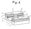
- Fig. 6 is a perspective cross sectional view showing a light emitting diode in accordance with the prior art.
- a prior art edge-emitting LED comprises a p-InP substrate 1, an n-InP block layer 2, a p-InP block layer 3, a p-InP cladding layer 4, active layers 5, 8, a p-InGaAsP light emitting region A, an n-InGaAsP contact layer 7, a p-InGaAsP optical absorption region B, and an SiO 2 film 9.
- the prior art edge emitting LED has an optical absorption region B separated from the light emitting region A and the InP block layer 6.
- a backward light emitted in the light emitting region A is propagated to the InP block layer 6 with some radiation angles due to diffraction, through the optical absorption region B.
- the backward light combines with the optical absorption region B. Since an effective bandgap of the optical absorption region B is smaller than that of the light emitting region A, the light combined with the optical absorption region B decreases due to an optical absorption effect.
- an edge emitting LED as defined in claim 1.
- the present invention is also directed to a method of forming a light emitting diode.
- Fig. 1 is a perspective view showing an edge emitting LED according to an embodiment of the present invention.
- Fig. 2 is a cross sectional view showing an edge emitting LED according to an embodiment of the present invention.
- Fig. 3 is a cross sectional view taken on line A-A of Fig. 2.
- an edge emitting LED comprises an n-InP substrate 11, an n-InP cladding layer 12 formed on the n-InP substrate 11, an active layer 13 formed on the n-InP cladding layer 12, an n-InP cladding layer 14 formed on the active layer 13, first and second p-InP block layers 15 formed on the n-InP substrate 11 and is an optical confinement layer, a first n-InP block layer 16 formed on the first p-InP block layer 15, a second n-InP block layer 16 formed on the second p-InP block layer 15, a p-InGaAs contact layer 17 formed on the n-InP cladding layer 14 and the n-InP block layers 16, a p-electrode 18 formed on the p-InGaAs contact layer 17, and an n-electrode 19 formed under the n-InP substrate 11.
- the active layer 13 comprises a multiple quantum well layer having a stripe-geometry and is sandwiched between the first p-InP block layer 15 and the second p-InP block layer 16.
- the multiple quantum well layer 13 has a light emitting region 13A, an optical absorption region 13B and a composition change region 13C between the light emitting region A and the optical absorption region 13B.
- the thickness of the optical absorption region 13B is thicker than that of the light emitting region 13A.
- the thickness and composition of the multiple quantum well layer 13 located in the composition change region 13C continuously changes from the light emitting region 13A to the optical absorption region 13B. Therefore, the optical absorption region 13B has a bandgap energy smaller than that of the light emitting region 13A, and the bandgap energy of the composition change region 13C continuously changes.
- the light emitting region 13A and the optical absorption region 13B adopted in the multiple quantum well layer 13 comprises seven pieces of a well layer having the bandgap energy of 1.38 ⁇ m and the thickness of 7nm, and a barrier layer having the bandgap energy of 1.10 ⁇ m and the thickness of 10nm.
- the p-electrode 18 selectively is only located over the light emitting region 13A to confine a driving current to the emission regions.
- a length of the p-electrode 18 in an extension direction of the multiple quantum well layer 13 is shorter than that of the light emitting region 13A. Therefore, the present invention is able to prevent that a current is injected into the optical absorption region 13C in order to expand the current.
- the multiple quantum well layer 13 is buried in the p-InP block layer 15 and the n-InP block layer 16, very small emission spot size can be achieved.
- a backward light propagates to the optical absorption region 13B.
- Continuous refractive index change between the light emitting region 13A and the optical absorption region 13B prevents from a reflection and a diffraction.
- the backward light decreases by an absorption because of a bandgap energy of the optical absorption region 13B.
- a composition of the optical absorption region 13B lowers a bandgap energy to the emission wavelength, multiple reflections in the back facets of the optical absorption region 13B can be completely prevented.
- an edge emitting LED of the present invention is able to produce a stable, spontaneous emission of light under a wide range of operating conditions.
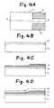
- Fig. 4 is a plane view and a cross sectional view showing an edge emitting LED according to a embodiment of the present invention for forming the edge emitting LED.
- the process for fabricating the edge emitting LED of the present invention is as follows:
- the n-InP substrate 11 has a previous formation region of an active layer 13 having a light emitting region 13A and an optical absorption region 13B continued with the light emitting region 13A.
- the active layer 13 comprises a InGaAsP/InGaAsP multiple quantum well structure.
- a first mask pattern 21 (for example a dielectric film, SiO 2 ) is selectively formed on the n-InP substrate 11 surface on both sides of the optical absorption region 13B.
- an n-InP cladding layer 12 is formed on the n-InP substrate 11 as is the first mask pattern 21, using a metalorganic vapor phase epitaxial (MOVPE).
- MOVPE metalorganic vapor phase epitaxial
- the precursors for group III and V are trimethylindium and PH 3 , and the dopant is Si 2 H 6 .
- an InGaAsP/InGaAsP multiple quantum well layer 13 is formed on the n-InP clad layer 12, using an MOVPE.
- the precursors for group III and V are trimethylindium, triethylgallium, AsH 3 and PH 3 , the dopant is DMZn, and a typical growth velocity is 0.8 ⁇ m/hour and a growth temperature is 630°C at 7.33 kPa (55 torr).
- a n-InP cladding layer 14 is formed on the multiple quantum well layer 13, using an MOVPE.
- the precursors for group III and V are trimethylindium and PH 3 and the dopant is DMZn.
- the first mask pattern 21 is removed from the structure formed by the steps.
- a second mask pattern 22 (for example a dielectric film, SiO 2 ) is then selectively formed on the n-InP cladding layer 14 over the formation region.
- the shape of the second mask pattern 22 is a straight line.
- the n-InP cladding layer 12, the multiple quantum well layer 13 and the n-InP cladding layer 14, are etched using the second mask pattern 22.
- a p-InP block layer 15 is formed on the n-InP substrate 11 in the removed portion, using an MOVPE.
- the precursors for group III and V are trimethylindium and PH 3 and the dopant is DMZn.
- an n-InP block layer 16 is formed on the p-InP block layer 15, using a MOVPE.
- the precursors for group III and V are trimethylindium and PH 3 , and the dopant is Si 2 H 6 .
- the second mask pattern is removed from the structure formed by the steps.
- a p-InGaAs contact layer 17 is formed on the n-InP clad layer 14 and the n-InP block layer 16, using an MOVPE.
- the precursors for group III and V are trimethylindium, triethylgallium and AsH 3 , and the dopant is DMZn.
- the p-electrode 18 is selectively only formed on the p-InGaAs contact layer 17 over the light emitting region 13A to confine a driving current to the emission region.
- the n-electrode 19 is formed under the n-InP substrate 11.
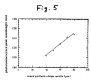
- Fig. 5 shows dependence of a bandgap energy on a mask pattern stripe.
- a method of forming a device for a measurement as follows:
- the n-InP substrate 11 has a first region and a second region continued with the first region.
- a mask pattern for example a dielectric film, SiO 2 ) is selectively formed on the n-InP substrate surface on both sides of the second region.
- an InGaAsP/InGaAsP multiple quantum well layer is formed on the n-InP substrate, using an MOVPE.
- the precursors for group III and V are trimethylindium, triethylgallium, AsH3 and PH3, the dopant is DMZn, and a typical growth velocity is 0.8 ⁇ m/hour and a growth temperature is 630°C at 7.33 kPa (55 torr).
- Measured data of the device is as follows:
- a multiple quantum well layer having a different photoluminesence peak wavelength/ a different bandgap energy/ a different thickness is selectively able to provide, with one-step growth, because of a mask pattern previously formed on the semiconductor substrate and after a multiple quantum well layer forms on the formed structure.
- a bandgap energy of a multiple quantum well layer formed in the optical absorption region can be controlled to be smaller than that of a multiple quantum well layer formed in the light emitting region because the first region is applied to a light emitting region and the second region is applied to an optical absorption region.
- the method of forming an edge emitting LED is capable of forming a light emitting region and an optical absorption region having differing compositions and thickness, with one-step growth.
- the present invention applied selective growth to the optical absorption region of the multiple quantum well layer.
- the present invention applies control effective reflection at the back facet of the light emitting device.
- the present invention may be apply in order to reduce a reflection.
- the present invention may be apply a RWG structure, a DC-PBH structure, a BC structure, and a MTBH structure.
Landscapes
- Chemical & Material Sciences (AREA)
- Health & Medical Sciences (AREA)
- Toxicology (AREA)
- Chemical Kinetics & Catalysis (AREA)
- Engineering & Computer Science (AREA)
- Materials Engineering (AREA)
- Mechanical Engineering (AREA)
- Metallurgy (AREA)
- Organic Chemistry (AREA)
- Led Devices (AREA)
- Semiconductor Lasers (AREA)
Claims (10)
- Diode électroluminescente à émission latérale ayant une région d'absorption optique à croissance dans une zone sélective, comprenant :un substrat semiconducteur (11) ayant une surface principale et une surface arrière;une couche active (13) formée sur la surface principale, la couche active (13) ayant une région d'émission de lumière (13A), une région d'absorption optique (13B) ayant une énergie de bande interdite inférieure à celle de la région d'émission de lumière (13A), et une région de changement de composition (13C) formée entre la région d'émission de lumière et la région d'absorption optique;une première électrode (19) formée sur la surface arrière du substrat semiconducteur; caractérisée parune seconde électrode (18) formée sur la région d'émission de lumière (13A), la seconde électrode (18) ayant une longueur inférieure à celle de la région d'émission de lumière (13A); etla région de changement de composition (13C) ayant une énergie de bande interdite qui change de façon continue.
- Diode électroluminescente à émission latérale selon la revendication 1, comprenant en outre :une première couche de gaine (12) formée sur la surface principale, avec la couche active (13) formée sur la première couche de gaine (12);une seconde couche de gaine (14) formée sur la couche active (13); etdes couches de confinement optique (15) entre lesquelles la couche active (13) est intercalée.
- Diode électroluminescente à émission latérale selon la revendication 1, dans laquelle la couche active (13) a une structure à puits quantiques multiples.
- Diode électroluminescente à émission latérale selon la revendication 2, dans laquelle le substrat semiconducteur (11) consiste en InP d'un premier type de conductivité, la première couche de gaine (12) consiste en InP du premier type de conductivité, la seconde couche de gaine (14) consiste en InP d'un second type de conductivité, et la couche de confinement optique (15) comprend des première et seconde couches de blocage en InP.
- Diode électroluminescente à émission par la tranche selon la revendication 3, dans laquelle la structure à puits quantiques multiples consiste en InGaAsP/InGaAsP.
- Procédé de formation d'une diode électroluminescente à émission latérale, comprenant :dans lequel la couche active (13) est une structure continue ayant une région d'émission de lumière (13A), une région d'absorption optique (13B) et une région de changement de composition (13C) formée entre la région d'émission de lumière et la région d'absorption optique, etla formation d'un motif de masque (21) sur une surface principale d'un substrat (11) des deux côtés d'une zone sélectionnée pour la croissance d'une région d'absorption optique (13B);la formation d'une couche active (13) sur la surface principale du substrat (11),
la formation d'une première électrode (19) sur la surface arrière du substrat (11); caractérisé par
la formation de la région d'absorption optique par croissance dans une zone sélective; et
la formation d'une seconde électrode (18) ayant une longueur inférieure à celle de la région d'émission de lumière (13A), sur la région d'émission de lumière (13A). - Procédé selon la revendication 6, dans lequel la couche active (13) comprend une structure à puits quantiques multiples.
- Procédé selon la revendication 6, dans lequel l'étape de formation de la couche active (13) utilise une épitaxie en phase vapeur aux organométalliques.
- Procédé selon la revendication 6, dans lequel le substrat semiconducteur consiste en InP d'un premier type de conductivité, une première couche de gaine (12) consiste en InP du premier type de conductivité, et une seconde couche de gaine (14) consiste en InP d'un second type de conductivité.
- Procédé selon la revendication 7, dans lequel la couche quantique multiple consiste en InGaAsP/InGaAsP.
Applications Claiming Priority (3)
| Application Number | Priority Date | Filing Date | Title |
|---|---|---|---|
| JP3934896 | 1996-02-27 | ||
| JP3934896A JPH09232625A (ja) | 1996-02-27 | 1996-02-27 | 端面発光型光半導体素子及びその製造方法 |
| JP39348/96 | 1996-02-27 |
Publications (2)
| Publication Number | Publication Date |
|---|---|
| EP0793280A1 EP0793280A1 (fr) | 1997-09-03 |
| EP0793280B1 true EP0793280B1 (fr) | 2002-05-15 |
Family
ID=12550583
Family Applications (1)
| Application Number | Title | Priority Date | Filing Date |
|---|---|---|---|
| EP19970103183 Expired - Lifetime EP0793280B1 (fr) | 1996-02-27 | 1997-02-27 | LED à émission latérale et sa méthode de fabrication |
Country Status (5)
| Country | Link |
|---|---|
| US (2) | US5889294A (fr) |
| EP (1) | EP0793280B1 (fr) |
| JP (1) | JPH09232625A (fr) |
| KR (1) | KR970063768A (fr) |
| DE (1) | DE69712563T2 (fr) |
Families Citing this family (12)
| Publication number | Priority date | Publication date | Assignee | Title |
|---|---|---|---|---|
| JP2967737B2 (ja) * | 1996-12-05 | 1999-10-25 | 日本電気株式会社 | 光半導体装置とその製造方法 |
| JPH11121860A (ja) * | 1997-10-20 | 1999-04-30 | Oki Electric Ind Co Ltd | 化合物半導体発光素子およびその形成方法 |
| US6528337B1 (en) * | 1999-04-08 | 2003-03-04 | The Furukawa Electric Co., Ltd. | Process of producing semiconductor layer structure |
| US6944197B2 (en) * | 2001-06-26 | 2005-09-13 | University Of Maryland, Baltimore County | Low crosstalk optical gain medium and method for forming same |
| US6807214B2 (en) * | 2002-08-01 | 2004-10-19 | Agilent Technologies, Inc. | Integrated laser and electro-absorption modulator with improved extinction |
| CN100367586C (zh) * | 2003-05-23 | 2008-02-06 | 武汉光迅科技股份有限公司 | 铝镓铟砷多量子阱超辐射发光二极管 |
| CN100384038C (zh) * | 2004-09-16 | 2008-04-23 | 中国科学院半导体研究所 | 选择区域外延生长叠层电吸收调制激光器结构的制作方法 |
| US20060222264A1 (en) * | 2005-03-31 | 2006-10-05 | Siemens Ag | Method for vertically orienting a face shown in a picture |
| CN1296760C (zh) * | 2005-05-20 | 2007-01-24 | 深圳市中电淼浩固体光源有限公司 | 一种使用匀光器的led光源 |
| KR100884353B1 (ko) | 2007-09-18 | 2009-02-18 | 한국전자통신연구원 | 고휘도 다이오드 및 그 제조 방법 |
| EP2208393B1 (fr) * | 2007-11-01 | 2019-04-24 | Nxp B.V. | Ensemble del et procédé de fabrication de cet ensemble del |
| GB2580956B (en) * | 2019-01-31 | 2023-01-25 | Exalos Ag | Amplified Spontaneous Emission Semiconductor Source |
Family Cites Families (4)
| Publication number | Priority date | Publication date | Assignee | Title |
|---|---|---|---|---|
| JPH0277174A (ja) * | 1988-06-10 | 1990-03-16 | Toshiba Corp | 端面放射型発光ダイオード |
| EP0558089B1 (fr) * | 1992-02-28 | 2002-06-05 | Hitachi, Ltd. | Dispositif optique, intégré à semi-conducteur et méthode de fabrication, et récepteur de lumière utilisant ce dispositif |
| JPH0669538A (ja) * | 1992-08-21 | 1994-03-11 | Oki Electric Ind Co Ltd | 端面放射型発光ダイオード |
| JP2937751B2 (ja) * | 1994-04-28 | 1999-08-23 | 日本電気株式会社 | 光半導体装置の製造方法 |
-
1996
- 1996-02-27 JP JP3934896A patent/JPH09232625A/ja active Pending
-
1997
- 1997-02-19 KR KR1019970004955A patent/KR970063768A/ko not_active Abandoned
- 1997-02-25 US US08/805,716 patent/US5889294A/en not_active Expired - Fee Related
- 1997-02-27 EP EP19970103183 patent/EP0793280B1/fr not_active Expired - Lifetime
- 1997-02-27 DE DE69712563T patent/DE69712563T2/de not_active Expired - Fee Related
-
1998
- 1998-01-07 US US09/003,694 patent/US6013539A/en not_active Expired - Fee Related
Also Published As
| Publication number | Publication date |
|---|---|
| US6013539A (en) | 2000-01-11 |
| KR970063768A (ko) | 1997-09-12 |
| JPH09232625A (ja) | 1997-09-05 |
| DE69712563T2 (de) | 2002-12-19 |
| US5889294A (en) | 1999-03-30 |
| DE69712563D1 (de) | 2002-06-20 |
| EP0793280A1 (fr) | 1997-09-03 |
Similar Documents
| Publication | Publication Date | Title |
|---|---|---|
| US6426515B2 (en) | Semiconductor light-emitting device | |
| JPH08107251A (ja) | 反射ディジタル同調レーザの作製方法 | |
| EP0526128B1 (fr) | Procédé pour la production d'un laser à semi-conducteur à réaction distribuée | |
| EP0177221B1 (fr) | Laser à semi-conducteur | |
| US5636237A (en) | Semiconductor laser device which makes it possible to realize high-speed modulation | |
| US5847415A (en) | Light emitting device having current blocking structure | |
| US6013539A (en) | Edge emitting led and method of forming the same | |
| EP0680119B1 (fr) | Procédé de fabrication d'un dispositif optique à semi-conducteur | |
| KR100632308B1 (ko) | 이득결합 분포귀환형 반도체레이저장치 및 그의 제조방법 | |
| US6678302B2 (en) | Semiconductor device and manufacturing method thereof | |
| EP1227556A2 (fr) | Dispositif laser à semi-conducteur à réaction distribuée à couplage complexe | |
| JP2001156391A (ja) | 光半導体装置およびその製造方法 | |
| US5465266A (en) | Index-guided laser on a ridged (001) substrate | |
| EP1233489A2 (fr) | Dispositif laser à semiconducteur du type DFB | |
| KR100305301B1 (ko) | 광반도체장치의제조방법 | |
| JP2998629B2 (ja) | 光半導体装置とその製造方法 | |
| JPH08307012A (ja) | 選択成長用マスク,半導体光装置の製造方法,および半導体光装置 | |
| US5469459A (en) | Laser diode element with excellent intermodulation distortion characteristic | |
| EP1130714A2 (fr) | Eléments laser à longueurs d'onde différentes sur un seul substrat | |
| US5400356A (en) | Index-guided laser on grooved (001) substrate | |
| US5828085A (en) | Light emitting diode having light-emitting and light-absorbing regions | |
| JP2763090B2 (ja) | 半導体レーザ装置及びその製造方法、ならびに結晶成長方法 | |
| US5360763A (en) | Method for fabricating an optical semiconductor device | |
| JP2000353849A (ja) | 光半導体装置およびその製造方法 | |
| US7050472B2 (en) | Semiconductor laser device and method for manufacturing the same |
Legal Events
| Date | Code | Title | Description |
|---|---|---|---|
| PUAI | Public reference made under article 153(3) epc to a published international application that has entered the european phase |
Free format text: ORIGINAL CODE: 0009012 |
|
| AK | Designated contracting states |
Kind code of ref document: A1 Designated state(s): DE FR GB |
|
| 17P | Request for examination filed |
Effective date: 19971105 |
|
| 17Q | First examination report despatched |
Effective date: 19990617 |
|
| GRAG | Despatch of communication of intention to grant |
Free format text: ORIGINAL CODE: EPIDOS AGRA |
|
| RTI1 | Title (correction) |
Free format text: AN EDGE EMITTING LED AND METHOD OF FORMING THE SAME |
|
| GRAG | Despatch of communication of intention to grant |
Free format text: ORIGINAL CODE: EPIDOS AGRA |
|
| GRAH | Despatch of communication of intention to grant a patent |
Free format text: ORIGINAL CODE: EPIDOS IGRA |
|
| GRAH | Despatch of communication of intention to grant a patent |
Free format text: ORIGINAL CODE: EPIDOS IGRA |
|
| GRAA | (expected) grant |
Free format text: ORIGINAL CODE: 0009210 |
|
| AK | Designated contracting states |
Kind code of ref document: B1 Designated state(s): DE FR GB |
|
| REG | Reference to a national code |
Ref country code: GB Ref legal event code: FG4D |
|
| REF | Corresponds to: |
Ref document number: 69712563 Country of ref document: DE Date of ref document: 20020620 |
|
| ET | Fr: translation filed | ||
| PGFP | Annual fee paid to national office [announced via postgrant information from national office to epo] |
Ref country code: FR Payment date: 20030210 Year of fee payment: 7 |
|
| PGFP | Annual fee paid to national office [announced via postgrant information from national office to epo] |
Ref country code: GB Payment date: 20030226 Year of fee payment: 7 |
|
| PGFP | Annual fee paid to national office [announced via postgrant information from national office to epo] |
Ref country code: DE Payment date: 20030306 Year of fee payment: 7 |
|
| PLBE | No opposition filed within time limit |
Free format text: ORIGINAL CODE: 0009261 |
|
| STAA | Information on the status of an ep patent application or granted ep patent |
Free format text: STATUS: NO OPPOSITION FILED WITHIN TIME LIMIT |
|
| 26N | No opposition filed |
Effective date: 20030218 |
|
| PG25 | Lapsed in a contracting state [announced via postgrant information from national office to epo] |
Ref country code: GB Free format text: LAPSE BECAUSE OF NON-PAYMENT OF DUE FEES Effective date: 20040227 |
|
| PG25 | Lapsed in a contracting state [announced via postgrant information from national office to epo] |
Ref country code: DE Free format text: LAPSE BECAUSE OF NON-PAYMENT OF DUE FEES Effective date: 20040901 |
|
| GBPC | Gb: european patent ceased through non-payment of renewal fee | ||
| PG25 | Lapsed in a contracting state [announced via postgrant information from national office to epo] |
Ref country code: FR Free format text: LAPSE BECAUSE OF NON-PAYMENT OF DUE FEES Effective date: 20041029 |
|
| REG | Reference to a national code |
Ref country code: FR Ref legal event code: ST |