EP0794553A2 - Réacteur à plasma de haute densité pour la cvd et la gravure - Google Patents
Réacteur à plasma de haute densité pour la cvd et la gravure Download PDFInfo
- Publication number
- EP0794553A2 EP0794553A2 EP97106424A EP97106424A EP0794553A2 EP 0794553 A2 EP0794553 A2 EP 0794553A2 EP 97106424 A EP97106424 A EP 97106424A EP 97106424 A EP97106424 A EP 97106424A EP 0794553 A2 EP0794553 A2 EP 0794553A2
- Authority
- EP
- European Patent Office
- Prior art keywords
- wafer
- plasma
- reactor
- antenna
- chamber
- Prior art date
- Legal status (The legal status is an assumption and is not a legal conclusion. Google has not performed a legal analysis and makes no representation as to the accuracy of the status listed.)
- Withdrawn
Links
Images


Classifications
-
- H—ELECTRICITY
- H05—ELECTRIC TECHNIQUES NOT OTHERWISE PROVIDED FOR
- H05H—PLASMA TECHNIQUE; PRODUCTION OF ACCELERATED ELECTRICALLY-CHARGED PARTICLES OR OF NEUTRONS; PRODUCTION OR ACCELERATION OF NEUTRAL MOLECULAR OR ATOMIC BEAMS
- H05H1/00—Generating plasma; Handling plasma
- H05H1/24—Generating plasma
- H05H1/26—Plasma torches
-
- H—ELECTRICITY
- H05—ELECTRIC TECHNIQUES NOT OTHERWISE PROVIDED FOR
- H05H—PLASMA TECHNIQUE; PRODUCTION OF ACCELERATED ELECTRICALLY-CHARGED PARTICLES OR OF NEUTRONS; PRODUCTION OR ACCELERATION OF NEUTRAL MOLECULAR OR ATOMIC BEAMS
- H05H1/00—Generating plasma; Handling plasma
- H05H1/24—Generating plasma
- H05H1/46—Generating plasma using applied electromagnetic fields, e.g. high frequency or microwave energy
-
- H—ELECTRICITY
- H01—ELECTRIC ELEMENTS
- H01J—ELECTRIC DISCHARGE TUBES OR DISCHARGE LAMPS
- H01J37/00—Discharge tubes with provision for introducing objects or material to be exposed to the discharge, e.g. for the purpose of examination or processing thereof
- H01J37/32—Gas-filled discharge tubes
- H01J37/32009—Arrangements for generation of plasma specially adapted for examination or treatment of objects, e.g. plasma sources
- H01J37/32082—Radio frequency generated discharge
- H01J37/321—Radio frequency generated discharge the radio frequency energy being inductively coupled to the plasma
-
- H—ELECTRICITY
- H01—ELECTRIC ELEMENTS
- H01J—ELECTRIC DISCHARGE TUBES OR DISCHARGE LAMPS
- H01J37/00—Discharge tubes with provision for introducing objects or material to be exposed to the discharge, e.g. for the purpose of examination or processing thereof
- H01J37/32—Gas-filled discharge tubes
- H01J37/32431—Constructional details of the reactor
- H01J37/3244—Gas supply means
Definitions
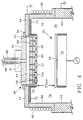
- the ground plane provided by the dome-shaped ceiling 116 is further away from the wafer surface at the wafer center than at the wafer edges so as to enhance ion density near the wafer center by providing more volume for ion diffusion to even out non-uniformites, thereby increasing ion density uniformity across the wafer surface.
- the dome-shaped conductive ceiling 116 of FIG. 11 has a major radius R 1 of 10.42 inch (26.05 cm) and a horizontal diameter D of 12.25 inch (30.6 cm).
- the dome-shaped ceiling 116 is supported by shoulders 116a resting on the vertical vacuum chamber wall 114 so that the top of the dome ceiling 116 rises about 5 inches (12.5 cm) above the wafer, similarly to the embodiment of FIG. 6.
- FIG. 6 As in the embodiment of FIG.
Landscapes
- Physics & Mathematics (AREA)
- Engineering & Computer Science (AREA)
- Plasma & Fusion (AREA)
- Chemical & Material Sciences (AREA)
- Analytical Chemistry (AREA)
- Spectroscopy & Molecular Physics (AREA)
- Electromagnetism (AREA)
- Chemical Vapour Deposition (AREA)
- Drying Of Semiconductors (AREA)
- Physical Vapour Deposition (AREA)
- ing And Chemical Polishing (AREA)
- Plasma Technology (AREA)
Applications Claiming Priority (3)
| Application Number | Priority Date | Filing Date | Title |
|---|---|---|---|
| US08/113,776 US5614055A (en) | 1993-08-27 | 1993-08-27 | High density plasma CVD and etching reactor |
| US113776 | 1993-08-27 | ||
| EP94305090A EP0641013B1 (fr) | 1993-08-27 | 1994-07-12 | Système d'injection de gaz dans un réacteur à plasma |
Related Parent Applications (2)
| Application Number | Title | Priority Date | Filing Date |
|---|---|---|---|
| EP94305090.6 Division | 1994-07-12 | ||
| EP94305090A Division EP0641013B1 (fr) | 1993-08-27 | 1994-07-12 | Système d'injection de gaz dans un réacteur à plasma |
Publications (2)
| Publication Number | Publication Date |
|---|---|
| EP0794553A2 true EP0794553A2 (fr) | 1997-09-10 |
| EP0794553A3 EP0794553A3 (fr) | 1998-05-20 |
Family
ID=22351456
Family Applications (2)
| Application Number | Title | Priority Date | Filing Date |
|---|---|---|---|
| EP97106424A Withdrawn EP0794553A3 (fr) | 1993-08-27 | 1994-07-12 | Réacteur à plasma de haute densité pour la cvd et la gravure |
| EP94305090A Expired - Lifetime EP0641013B1 (fr) | 1993-08-27 | 1994-07-12 | Système d'injection de gaz dans un réacteur à plasma |
Family Applications After (1)
| Application Number | Title | Priority Date | Filing Date |
|---|---|---|---|
| EP94305090A Expired - Lifetime EP0641013B1 (fr) | 1993-08-27 | 1994-07-12 | Système d'injection de gaz dans un réacteur à plasma |
Country Status (5)
| Country | Link |
|---|---|
| US (2) | US5614055A (fr) |
| EP (2) | EP0794553A3 (fr) |
| JP (1) | JP3691528B2 (fr) |
| KR (1) | KR100201121B1 (fr) |
| DE (1) | DE69425203T2 (fr) |
Cited By (1)
| Publication number | Priority date | Publication date | Assignee | Title |
|---|---|---|---|---|
| US6076482A (en) * | 1997-09-20 | 2000-06-20 | Applied Materials, Inc. | Thin film processing plasma reactor chamber with radially upward sloping ceiling for promoting radially outward diffusion |
Families Citing this family (382)
| Publication number | Priority date | Publication date | Assignee | Title |
|---|---|---|---|---|
| US6165311A (en) | 1991-06-27 | 2000-12-26 | Applied Materials, Inc. | Inductively coupled RF plasma reactor having an overhead solenoidal antenna |
| US6514376B1 (en) | 1991-06-27 | 2003-02-04 | Applied Materials Inc. | Thermal control apparatus for inductively coupled RF plasma reactor having an overhead solenoidal antenna |
| US6488807B1 (en) | 1991-06-27 | 2002-12-03 | Applied Materials, Inc. | Magnetic confinement in a plasma reactor having an RF bias electrode |
| US6036877A (en) | 1991-06-27 | 2000-03-14 | Applied Materials, Inc. | Plasma reactor with heated source of a polymer-hardening precursor material |
| US6063233A (en) | 1991-06-27 | 2000-05-16 | Applied Materials, Inc. | Thermal control apparatus for inductively coupled RF plasma reactor having an overhead solenoidal antenna |
| US6077384A (en) | 1994-08-11 | 2000-06-20 | Applied Materials, Inc. | Plasma reactor having an inductive antenna coupling power through a parallel plate electrode |
| US6095083A (en) * | 1991-06-27 | 2000-08-01 | Applied Materiels, Inc. | Vacuum processing chamber having multi-mode access |
| US6074512A (en) * | 1991-06-27 | 2000-06-13 | Applied Materials, Inc. | Inductively coupled RF plasma reactor having an overhead solenoidal antenna and modular confinement magnet liners |
| US5614055A (en) * | 1993-08-27 | 1997-03-25 | Applied Materials, Inc. | High density plasma CVD and etching reactor |
| US5865896A (en) | 1993-08-27 | 1999-02-02 | Applied Materials, Inc. | High density plasma CVD reactor with combined inductive and capacitive coupling |
| JP2687867B2 (ja) * | 1994-01-19 | 1997-12-08 | 日本電気株式会社 | 半導体製造装置 |
| ATE251798T1 (de) * | 1994-04-28 | 2003-10-15 | Applied Materials Inc | Verfahren zum betreiben eines cvd-reaktors hoher plasma-dichte mit kombinierter induktiver und kapazitiver einkopplung |
| JP3080843B2 (ja) * | 1994-08-24 | 2000-08-28 | 松下電器産業株式会社 | 薄膜形成方法及び装置 |
| US5753044A (en) * | 1995-02-15 | 1998-05-19 | Applied Materials, Inc. | RF plasma reactor with hybrid conductor and multi-radius dome ceiling |
| US5777289A (en) * | 1995-02-15 | 1998-07-07 | Applied Materials, Inc. | RF plasma reactor with hybrid conductor and multi-radius dome ceiling |
| US6270617B1 (en) * | 1995-02-15 | 2001-08-07 | Applied Materials, Inc. | RF plasma reactor with hybrid conductor and multi-radius dome ceiling |
| US5710486A (en) * | 1995-05-08 | 1998-01-20 | Applied Materials, Inc. | Inductively and multi-capacitively coupled plasma reactor |
| TW283250B (en) | 1995-07-10 | 1996-08-11 | Watkins Johnson Co | Plasma enhanced chemical processing reactor and method |
| JPH0925586A (ja) * | 1995-07-11 | 1997-01-28 | Anelva Corp | 基板処理装置および基板処理方法 |
| US5653811A (en) | 1995-07-19 | 1997-08-05 | Chan; Chung | System for the plasma treatment of large area substrates |
| TW279240B (en) | 1995-08-30 | 1996-06-21 | Applied Materials Inc | Parallel-plate icp source/rf bias electrode head |
| KR100197649B1 (ko) * | 1995-09-29 | 1999-06-15 | 김영환 | 박막 증착장치 |
| TW356554B (en) * | 1995-10-23 | 1999-04-21 | Watkins Johnson Co | Gas injection system for semiconductor processing |
| US5772771A (en) | 1995-12-13 | 1998-06-30 | Applied Materials, Inc. | Deposition chamber for improved deposition thickness uniformity |
| US6054013A (en) * | 1996-02-02 | 2000-04-25 | Applied Materials, Inc. | Parallel plate electrode plasma reactor having an inductive antenna and adjustable radial distribution of plasma ion density |
| US6036878A (en) | 1996-02-02 | 2000-03-14 | Applied Materials, Inc. | Low density high frequency process for a parallel-plate electrode plasma reactor having an inductive antenna |
| JP3720901B2 (ja) * | 1996-03-04 | 2005-11-30 | アネルバ株式会社 | プラズマ処理装置及びアンテナの製造方法 |
| WO1997033300A1 (fr) * | 1996-03-06 | 1997-09-12 | Mattson Technology, Inc. | Reacteur a plasma inductif a section generatrice de plasma de forme conique |
| US6017825A (en) * | 1996-03-29 | 2000-01-25 | Lam Research Corporation | Etch rate loading improvement |
| US6070551A (en) | 1996-05-13 | 2000-06-06 | Applied Materials, Inc. | Deposition chamber and method for depositing low dielectric constant films |
| US5863376A (en) * | 1996-06-05 | 1999-01-26 | Lam Research Corporation | Temperature controlling method and apparatus for a plasma processing chamber |
| JP4195734B2 (ja) | 1996-06-10 | 2008-12-10 | テキサス インスツルメンツ インコーポレイテツド | 集積回路のトレンチ分離製作方法 |
| AU3145197A (en) * | 1996-06-28 | 1998-01-21 | Lam Research Corporation | Apparatus and method for high density plasma chemical vapor deposition |
| US6013155A (en) * | 1996-06-28 | 2000-01-11 | Lam Research Corporation | Gas injection system for plasma processing |
| US6056848A (en) * | 1996-09-11 | 2000-05-02 | Ctp, Inc. | Thin film electrostatic shield for inductive plasma processing |
| JP3640478B2 (ja) * | 1996-09-20 | 2005-04-20 | アネルバ株式会社 | プラズマ処理装置 |
| US5911832A (en) * | 1996-10-10 | 1999-06-15 | Eaton Corporation | Plasma immersion implantation with pulsed anode |
| US6020035A (en) | 1996-10-29 | 2000-02-01 | Applied Materials, Inc. | Film to tie up loose fluorine in the chamber after a clean process |
| US5804259A (en) * | 1996-11-07 | 1998-09-08 | Applied Materials, Inc. | Method and apparatus for depositing a multilayered low dielectric constant film |
| TW403959B (en) * | 1996-11-27 | 2000-09-01 | Hitachi Ltd | Plasma treatment device |
| US6367410B1 (en) | 1996-12-16 | 2002-04-09 | Applied Materials, Inc. | Closed-loop dome thermal control apparatus for a semiconductor wafer processing system |
| US6033585A (en) * | 1996-12-20 | 2000-03-07 | Lam Research Corporation | Method and apparatus for preventing lightup of gas distribution holes |
| US6184158B1 (en) * | 1996-12-23 | 2001-02-06 | Lam Research Corporation | Inductively coupled plasma CVD |
| KR100252210B1 (ko) * | 1996-12-24 | 2000-04-15 | 윤종용 | 반도체장치 제조용 건식식각장치 |
| US6749717B1 (en) | 1997-02-04 | 2004-06-15 | Micron Technology, Inc. | Device for in-situ cleaning of an inductively-coupled plasma chambers |
| US5965218A (en) * | 1997-03-18 | 1999-10-12 | Vlsi Technology, Inc. | Process for manufacturing ultra-sharp atomic force microscope (AFM) and scanning tunneling microscope (STM) tips |
| EP0887847A1 (fr) | 1997-04-15 | 1998-12-30 | STMicroelectronics S.r.l. | Procédé de passivation finale de circuits intégrés |
| EP0872879A1 (fr) * | 1997-04-15 | 1998-10-21 | STMicroelectronics S.r.l. | Procédé de passivation finale d'un dispositif à circuit intégré |
| US6579426B1 (en) | 1997-05-16 | 2003-06-17 | Applied Materials, Inc. | Use of variable impedance to control coil sputter distribution |
| US6286451B1 (en) * | 1997-05-29 | 2001-09-11 | Applied Materials, Inc. | Dome: shape and temperature controlled surfaces |
| TW460943B (en) * | 1997-06-11 | 2001-10-21 | Applied Materials Inc | Reduction of mobile ion and metal contamination in HDP-CVD chambers using chamber seasoning film depositions |
| US5872058A (en) * | 1997-06-17 | 1999-02-16 | Novellus Systems, Inc. | High aspect ratio gapfill process by using HDP |
| US6042687A (en) * | 1997-06-30 | 2000-03-28 | Lam Research Corporation | Method and apparatus for improving etch and deposition uniformity in plasma semiconductor processing |
| US6345588B1 (en) | 1997-08-07 | 2002-02-12 | Applied Materials, Inc. | Use of variable RF generator to control coil voltage distribution |
| JP2001514444A (ja) | 1997-08-26 | 2001-09-11 | アプライド マテリアルズ インコーポレイテッド | プラズマ処理チャンバへ安定した電力を送ることができる装置及び方法 |
| US6565717B1 (en) * | 1997-09-15 | 2003-05-20 | Applied Materials, Inc. | Apparatus for sputtering ionized material in a medium to high density plasma |
| US6132551A (en) * | 1997-09-20 | 2000-10-17 | Applied Materials, Inc. | Inductive RF plasma reactor with overhead coil and conductive laminated RF window beneath the overhead coil |
| US5903106A (en) * | 1997-11-17 | 1999-05-11 | Wj Semiconductor Equipment Group, Inc. | Plasma generating apparatus having an electrostatic shield |
| US6028285A (en) * | 1997-11-19 | 2000-02-22 | Board Of Regents, The University Of Texas System | High density plasma source for semiconductor processing |
| US5976900A (en) * | 1997-12-08 | 1999-11-02 | Cypress Semiconductor Corp. | Method of reducing impurity contamination in semiconductor process chambers |
| US20020011215A1 (en) | 1997-12-12 | 2002-01-31 | Goushu Tei | Plasma treatment apparatus and method of manufacturing optical parts using the same |
| KR100524204B1 (ko) * | 1998-01-07 | 2006-01-27 | 동경 엘렉트론 주식회사 | 가스 처리장치 |
| US6015476A (en) * | 1998-02-05 | 2000-01-18 | Applied Materials, Inc. | Plasma reactor magnet with independently controllable parallel axial current-carrying elements |
| US6274459B1 (en) | 1998-02-17 | 2001-08-14 | Silicon Genesis Corporation | Method for non mass selected ion implant profile control |
| US6022749A (en) * | 1998-02-25 | 2000-02-08 | Advanced Micro Devices, Inc. | Using a superlattice to determine the temperature of a semiconductor fabrication process |
| JP2972707B1 (ja) | 1998-02-26 | 1999-11-08 | 松下電子工業株式会社 | プラズマエッチング装置及びプラズマエッチング方法 |
| US6189484B1 (en) * | 1999-03-05 | 2001-02-20 | Applied Materials Inc. | Plasma reactor having a helicon wave high density plasma source |
| US6194038B1 (en) * | 1998-03-20 | 2001-02-27 | Applied Materials, Inc. | Method for deposition of a conformal layer on a substrate |
| US6203657B1 (en) | 1998-03-31 | 2001-03-20 | Lam Research Corporation | Inductively coupled plasma downstream strip module |
| CN1189595C (zh) | 1998-04-13 | 2005-02-16 | 东京电子株式会社 | 阻抗减小的室 |
| US6269278B1 (en) | 1998-04-23 | 2001-07-31 | Sandia Corporation | Method and apparatus for monitoring plasma processing operations |
| US6261470B1 (en) | 1998-04-23 | 2001-07-17 | Sandia Corporation | Method and apparatus for monitoring plasma processing operations |
| US6123983A (en) * | 1998-04-23 | 2000-09-26 | Sandia Corporation | Method and apparatus for monitoring plasma processing operations |
| US6221679B1 (en) * | 1998-04-23 | 2001-04-24 | Sandia Corporation | Method and apparatus for monitoring plasma processing operations |
| US6090302A (en) * | 1998-04-23 | 2000-07-18 | Sandia | Method and apparatus for monitoring plasma processing operations |
| US6169933B1 (en) | 1998-04-23 | 2001-01-02 | Sandia Corporation | Method and apparatus for monitoring plasma processing operations |
| US6132577A (en) * | 1998-04-23 | 2000-10-17 | Sandia Corporation | Method and apparatus for monitoring plasma processing operations |
| US6419801B1 (en) | 1998-04-23 | 2002-07-16 | Sandia Corporation | Method and apparatus for monitoring plasma processing operations |
| US6134005A (en) * | 1998-04-23 | 2000-10-17 | Sandia Corporation | Method and apparatus for monitoring plasma processing operations |
| US6223755B1 (en) | 1998-04-23 | 2001-05-01 | Sandia Corporation | Method and apparatus for monitoring plasma processing operations |
| US6165312A (en) * | 1998-04-23 | 2000-12-26 | Sandia Corporation | Method and apparatus for monitoring plasma processing operations |
| US6157447A (en) * | 1998-04-23 | 2000-12-05 | Sandia Corporation | Method and apparatus for monitoring plasma processing operations |
| US6246473B1 (en) | 1998-04-23 | 2001-06-12 | Sandia Corporation | Method and apparatus for monitoring plasma processing operations |
| US6192826B1 (en) | 1998-04-23 | 2001-02-27 | Sandia Corporation | Method and apparatus for monitoring plasma processing operations |
| US6254717B1 (en) | 1998-04-23 | 2001-07-03 | Sandia Corporation | Method and apparatus for monitoring plasma processing operations |
| US6077386A (en) * | 1998-04-23 | 2000-06-20 | Sandia Corporation | Method and apparatus for monitoring plasma processing operations |
| US6275740B1 (en) | 1998-04-23 | 2001-08-14 | Sandia Corporation | Method and apparatus for monitoring plasma processing operations |
| US6060132A (en) * | 1998-06-15 | 2000-05-09 | Siemens Aktiengesellschaft | High density plasma CVD process for making dielectric anti-reflective coatings |
| US6074516A (en) * | 1998-06-23 | 2000-06-13 | Lam Research Corporation | High sputter, etch resistant window for plasma processing chambers |
| US6037018A (en) * | 1998-07-01 | 2000-03-14 | Taiwan Semiconductor Maufacturing Company | Shallow trench isolation filled by high density plasma chemical vapor deposition |
| US6759306B1 (en) | 1998-07-10 | 2004-07-06 | Micron Technology, Inc. | Methods of forming silicon dioxide layers and methods of forming trench isolation regions |
| US6335293B1 (en) | 1998-07-13 | 2002-01-01 | Mattson Technology, Inc. | Systems and methods for two-sided etch of a semiconductor substrate |
| US6132566A (en) * | 1998-07-30 | 2000-10-17 | Applied Materials, Inc. | Apparatus and method for sputtering ionized material in a plasma |
| US6228208B1 (en) * | 1998-08-12 | 2001-05-08 | Applied Materials, Inc. | Plasma density and etch rate enhancing semiconductor processing chamber |
| US6074953A (en) * | 1998-08-28 | 2000-06-13 | Micron Technology, Inc. | Dual-source plasma etchers, dual-source plasma etching methods, and methods of forming planar coil dual-source plasma etchers |
| US6355183B1 (en) | 1998-09-04 | 2002-03-12 | Matsushita Electric Industrial Co., Ltd. | Apparatus and method for plasma etching |
| US6170429B1 (en) | 1998-09-30 | 2001-01-09 | Lam Research Corporation | Chamber liner for semiconductor process chambers |
| JP2000124195A (ja) * | 1998-10-14 | 2000-04-28 | Tokyo Electron Ltd | 表面処理方法及びその装置 |
| KR100303446B1 (ko) | 1998-10-29 | 2002-10-04 | 삼성전자 주식회사 | 액정표시장치용박막트랜지스터기판의제조방법 |
| US6324313B1 (en) * | 1998-12-21 | 2001-11-27 | Lsi Logic Corporation | On-chip multiple layer vertically transitioning optical waveguide and damascene method of fabricating the same |
| US6230651B1 (en) * | 1998-12-30 | 2001-05-15 | Lam Research Corporation | Gas injection system for plasma processing |
| JP3542514B2 (ja) * | 1999-01-19 | 2004-07-14 | 株式会社日立製作所 | ドライエッチング装置 |
| US6523493B1 (en) * | 2000-08-01 | 2003-02-25 | Tokyo Electron Limited | Ring-shaped high-density plasma source and method |
| US6458723B1 (en) | 1999-06-24 | 2002-10-01 | Silicon Genesis Corporation | High temperature implant apparatus |
| US6415736B1 (en) | 1999-06-30 | 2002-07-09 | Lam Research Corporation | Gas distribution apparatus for semiconductor processing |
| US6123775A (en) * | 1999-06-30 | 2000-09-26 | Lam Research Corporation | Reaction chamber component having improved temperature uniformity |
| US6245192B1 (en) | 1999-06-30 | 2001-06-12 | Lam Research Corporation | Gas distribution apparatus for semiconductor processing |
| US6447637B1 (en) * | 1999-07-12 | 2002-09-10 | Applied Materials Inc. | Process chamber having a voltage distribution electrode |
| US6451157B1 (en) | 1999-09-23 | 2002-09-17 | Lam Research Corporation | Gas distribution apparatus for semiconductor processing |
| US6462483B1 (en) * | 1999-11-18 | 2002-10-08 | Nano-Architect Research Corporation | Induction plasma processing chamber |
| KR20010062209A (ko) * | 1999-12-10 | 2001-07-07 | 히가시 데쓰로 | 고내식성 막이 내부에 형성된 챔버를 구비하는 처리 장치 |
| AU2577001A (en) * | 1999-12-22 | 2001-07-03 | Tokyo Electron Limited | Method and system for reducing damage to substrates during plasma processing with a resonator source |
| JP4437351B2 (ja) * | 2000-01-14 | 2010-03-24 | キヤノンアネルバ株式会社 | プラズマエッチング装置 |
| US6447636B1 (en) * | 2000-02-16 | 2002-09-10 | Applied Materials, Inc. | Plasma reactor with dynamic RF inductive and capacitive coupling control |
| JP4222707B2 (ja) * | 2000-03-24 | 2009-02-12 | 東京エレクトロン株式会社 | プラズマ処理装置及び方法、ガス供給リング及び誘電体 |
| US6502530B1 (en) * | 2000-04-26 | 2003-01-07 | Unaxis Balzers Aktiengesellschaft | Design of gas injection for the electrode in a capacitively coupled RF plasma reactor |
| US6401652B1 (en) | 2000-05-04 | 2002-06-11 | Applied Materials, Inc. | Plasma reactor inductive coil antenna with flat surface facing the plasma |
| KR20010112958A (ko) * | 2000-06-15 | 2001-12-24 | 황 철 주 | 고밀도 플라즈마 반응기 |
| US6481447B1 (en) * | 2000-09-27 | 2002-11-19 | Lam Research Corporation | Fluid delivery ring and methods for making and implementing the same |
| US6333272B1 (en) * | 2000-10-06 | 2001-12-25 | Lam Research Corporation | Gas distribution apparatus for semiconductor processing |
| US6413321B1 (en) | 2000-12-07 | 2002-07-02 | Applied Materials, Inc. | Method and apparatus for reducing particle contamination on wafer backside during CVD process |
| US6534423B1 (en) * | 2000-12-27 | 2003-03-18 | Novellus Systems, Inc. | Use of inductively-coupled plasma in plasma-enhanced chemical vapor deposition reactor to improve film-to-wall adhesion following in-situ plasma clean |
| US6660662B2 (en) * | 2001-01-26 | 2003-12-09 | Applied Materials, Inc. | Method of reducing plasma charge damage for plasma processes |
| JP2002237486A (ja) * | 2001-02-08 | 2002-08-23 | Tokyo Electron Ltd | プラズマ処理装置およびプラズマ処理方法 |
| JP2002246381A (ja) * | 2001-02-15 | 2002-08-30 | Anelva Corp | Cvd方法 |
| US6660126B2 (en) * | 2001-03-02 | 2003-12-09 | Applied Materials, Inc. | Lid assembly for a processing system to facilitate sequential deposition techniques |
| US20020122896A1 (en) * | 2001-03-02 | 2002-09-05 | Skion Corporation | Capillary discharge plasma apparatus and method for surface treatment using the same |
| KR100408405B1 (ko) * | 2001-05-03 | 2003-12-06 | 삼성전자주식회사 | 반도체 소자의 제조 장치 |
| US6596653B2 (en) * | 2001-05-11 | 2003-07-22 | Applied Materials, Inc. | Hydrogen assisted undoped silicon oxide deposition process for HDP-CVD |
| US6740601B2 (en) * | 2001-05-11 | 2004-05-25 | Applied Materials Inc. | HDP-CVD deposition process for filling high aspect ratio gaps |
| KR20040019293A (ko) | 2001-05-24 | 2004-03-05 | 셀레리티 그룹 아이엔씨 | 소정 비율의 프로세스 유체를 제공하는 방법 및 장치 |
| KR100585437B1 (ko) * | 2001-06-01 | 2006-06-07 | 동경 엘렉트론 주식회사 | 플라즈마 처리 장치 |
| US20020195201A1 (en) * | 2001-06-25 | 2002-12-26 | Emanuel Beer | Apparatus and method for thermally isolating a heat chamber |
| KR100433285B1 (ko) * | 2001-07-18 | 2004-05-31 | 주성엔지니어링(주) | 멀티 홀 앵글드 가스분사 시스템을 갖는 반도체소자제조장치 |
| WO2003023835A1 (fr) * | 2001-08-06 | 2003-03-20 | Genitech Co., Ltd. | Appareil de depot de couche atomique active par plasma (peald) et procede de formation d'un film mince a l'aide dudit appareil |
| US6820570B2 (en) * | 2001-08-15 | 2004-11-23 | Nobel Biocare Services Ag | Atomic layer deposition reactor |
| US6676760B2 (en) | 2001-08-16 | 2004-01-13 | Appiled Materials, Inc. | Process chamber having multiple gas distributors and method |
| JP3886424B2 (ja) * | 2001-08-28 | 2007-02-28 | 鹿児島日本電気株式会社 | 基板処理装置及び方法 |
| CN1316547C (zh) * | 2001-09-14 | 2007-05-16 | 东京电子株式会社 | 等离子体反应器线圈磁体系统 |
| US7115516B2 (en) * | 2001-10-09 | 2006-10-03 | Applied Materials, Inc. | Method of depositing a material layer |
| US20030070620A1 (en) | 2001-10-15 | 2003-04-17 | Cooperberg David J. | Tunable multi-zone gas injection system |
| KR100501339B1 (ko) * | 2001-11-02 | 2005-07-18 | 주성엔지니어링(주) | 플라즈마 장치 |
| KR100760291B1 (ko) * | 2001-11-08 | 2007-09-19 | 에이에스엠지니텍코리아 주식회사 | 박막 형성 방법 |
| KR100453014B1 (ko) * | 2001-12-26 | 2004-10-14 | 주성엔지니어링(주) | Cvd 장치 |
| US7513971B2 (en) * | 2002-03-18 | 2009-04-07 | Applied Materials, Inc. | Flat style coil for improved precision etch uniformity |
| GB0208261D0 (en) * | 2002-04-10 | 2002-05-22 | Dow Corning | An atmospheric pressure plasma assembly |
| US20040231798A1 (en) * | 2002-09-13 | 2004-11-25 | Applied Materials, Inc. | Gas delivery system for semiconductor processing |
| US6837966B2 (en) * | 2002-09-30 | 2005-01-04 | Tokyo Electron Limeted | Method and apparatus for an improved baffle plate in a plasma processing system |
| US7166166B2 (en) | 2002-09-30 | 2007-01-23 | Tokyo Electron Limited | Method and apparatus for an improved baffle plate in a plasma processing system |
| US7137353B2 (en) * | 2002-09-30 | 2006-11-21 | Tokyo Electron Limited | Method and apparatus for an improved deposition shield in a plasma processing system |
| US7147749B2 (en) * | 2002-09-30 | 2006-12-12 | Tokyo Electron Limited | Method and apparatus for an improved upper electrode plate with deposition shield in a plasma processing system |
| US7166200B2 (en) * | 2002-09-30 | 2007-01-23 | Tokyo Electron Limited | Method and apparatus for an improved upper electrode plate in a plasma processing system |
| US6798519B2 (en) * | 2002-09-30 | 2004-09-28 | Tokyo Electron Limited | Method and apparatus for an improved optical window deposition shield in a plasma processing system |
| US7204912B2 (en) * | 2002-09-30 | 2007-04-17 | Tokyo Electron Limited | Method and apparatus for an improved bellows shield in a plasma processing system |
| KR100488348B1 (ko) * | 2002-11-14 | 2005-05-10 | 최대규 | 플라즈마 프로세스 챔버 및 시스템 |
| TW200423195A (en) * | 2002-11-28 | 2004-11-01 | Tokyo Electron Ltd | Internal member of a plasma processing vessel |
| US7534363B2 (en) * | 2002-12-13 | 2009-05-19 | Lam Research Corporation | Method for providing uniform removal of organic material |
| US7169231B2 (en) * | 2002-12-13 | 2007-01-30 | Lam Research Corporation | Gas distribution system with tuning gas |
| US20040112540A1 (en) * | 2002-12-13 | 2004-06-17 | Lam Research Corporation | Uniform etch system |
| US7273638B2 (en) * | 2003-01-07 | 2007-09-25 | International Business Machines Corp. | High density plasma oxidation |
| US6808748B2 (en) * | 2003-01-23 | 2004-10-26 | Applied Materials, Inc. | Hydrogen assisted HDP-CVD deposition process for aggressive gap-fill technology |
| US20040173314A1 (en) * | 2003-03-05 | 2004-09-09 | Ryoji Nishio | Plasma processing apparatus and method |
| KR101016913B1 (ko) * | 2003-03-31 | 2011-02-22 | 도쿄엘렉트론가부시키가이샤 | 처리요소용 배리어층 및 그의 형성방법 |
| KR100918528B1 (ko) | 2003-03-31 | 2009-09-21 | 도쿄엘렉트론가부시키가이샤 | 처리부재 상에 인접한 코팅을 결합시키는 방법 |
| US6958112B2 (en) * | 2003-05-27 | 2005-10-25 | Applied Materials, Inc. | Methods and systems for high-aspect-ratio gapfill using atomic-oxygen generation |
| US20040261718A1 (en) * | 2003-06-26 | 2004-12-30 | Kim Nam Hun | Plasma source coil for generating plasma and plasma chamber using the same |
| US20050011447A1 (en) * | 2003-07-14 | 2005-01-20 | Tokyo Electron Limited | Method and apparatus for delivering process gas to a process chamber |
| US6829056B1 (en) | 2003-08-21 | 2004-12-07 | Michael Barnes | Monitoring dimensions of features at different locations in the processing of substrates |
| US6903031B2 (en) * | 2003-09-03 | 2005-06-07 | Applied Materials, Inc. | In-situ-etch-assisted HDP deposition using SiF4 and hydrogen |
| US20050103265A1 (en) * | 2003-11-19 | 2005-05-19 | Applied Materials, Inc., A Delaware Corporation | Gas distribution showerhead featuring exhaust apertures |
| KR100634288B1 (ko) * | 2003-12-01 | 2006-10-16 | 야스히로 모리 | 고체물질의 표면 개질방법 및 표면 개질된 고체물질 |
| US20050218115A1 (en) * | 2004-02-06 | 2005-10-06 | Applied Materials, Inc. | Anti-clogging nozzle for semiconductor processing |
| US20060048707A1 (en) * | 2004-09-03 | 2006-03-09 | Applied Materials, Inc. | Anti-clogging nozzle for semiconductor processing |
| US20050211544A1 (en) * | 2004-03-29 | 2005-09-29 | Seagate Technology Llc | Electrical biasing of gas introduction means of plasma apparatus |
| US8083853B2 (en) * | 2004-05-12 | 2011-12-27 | Applied Materials, Inc. | Plasma uniformity control by gas diffuser hole design |
| US20050233092A1 (en) * | 2004-04-20 | 2005-10-20 | Applied Materials, Inc. | Method of controlling the uniformity of PECVD-deposited thin films |
| US7785672B2 (en) * | 2004-04-20 | 2010-08-31 | Applied Materials, Inc. | Method of controlling the film properties of PECVD-deposited thin films |
| US7109114B2 (en) * | 2004-05-07 | 2006-09-19 | Applied Materials, Inc. | HDP-CVD seasoning process for high power HDP-CVD gapfil to improve particle performance |
| US8328939B2 (en) * | 2004-05-12 | 2012-12-11 | Applied Materials, Inc. | Diffuser plate with slit valve compensation |
| US8074599B2 (en) * | 2004-05-12 | 2011-12-13 | Applied Materials, Inc. | Plasma uniformity control by gas diffuser curvature |
| US20060005771A1 (en) * | 2004-07-12 | 2006-01-12 | Applied Materials, Inc. | Apparatus and method of shaping profiles of large-area PECVD electrodes |
| US20050260356A1 (en) * | 2004-05-18 | 2005-11-24 | Applied Materials, Inc. | Microcontamination abatement in semiconductor processing |
| US7229931B2 (en) * | 2004-06-16 | 2007-06-12 | Applied Materials, Inc. | Oxygen plasma treatment for enhanced HDP-CVD gapfill |
| US7183227B1 (en) | 2004-07-01 | 2007-02-27 | Applied Materials, Inc. | Use of enhanced turbomolecular pump for gapfill deposition using high flows of low-mass fluent gas |
| US7087536B2 (en) * | 2004-09-01 | 2006-08-08 | Applied Materials | Silicon oxide gapfill deposition using liquid precursors |
| US7429410B2 (en) * | 2004-09-20 | 2008-09-30 | Applied Materials, Inc. | Diffuser gravity support |
| KR100589046B1 (ko) * | 2004-09-23 | 2006-06-12 | 삼성전자주식회사 | 박막 형성 방법 |
| US7552521B2 (en) * | 2004-12-08 | 2009-06-30 | Tokyo Electron Limited | Method and apparatus for improved baffle plate |
| KR100610019B1 (ko) * | 2005-01-11 | 2006-08-08 | 삼성전자주식회사 | 플라즈마 분배장치 및 이를 구비하는 건식 스트리핑 장치 |
| US7601242B2 (en) * | 2005-01-11 | 2009-10-13 | Tokyo Electron Limited | Plasma processing system and baffle assembly for use in plasma processing system |
| US20060177600A1 (en) * | 2005-02-08 | 2006-08-10 | Applied Materials, Inc. | Inductive plasma system with sidewall magnet |
| US20060225654A1 (en) * | 2005-03-29 | 2006-10-12 | Fink Steven T | Disposable plasma reactor materials and methods |
| WO2006106764A1 (fr) * | 2005-03-30 | 2006-10-12 | Matsushita Electric Industrial Co., Ltd. | Ligne de transmission |
| US7396415B2 (en) * | 2005-06-02 | 2008-07-08 | Asm America, Inc. | Apparatus and methods for isolating chemical vapor reactions at a substrate surface |
| KR100698618B1 (ko) * | 2005-07-12 | 2007-03-22 | 삼성전자주식회사 | 플라즈마 가속장치 및 그것을 구비하는 플라즈마 처리시스템 |
| US8617672B2 (en) | 2005-07-13 | 2013-12-31 | Applied Materials, Inc. | Localized surface annealing of components for substrate processing chambers |
| US7651587B2 (en) | 2005-08-11 | 2010-01-26 | Applied Materials, Inc. | Two-piece dome with separate RF coils for inductively coupled plasma reactors |
| JP2007051002A (ja) * | 2005-08-19 | 2007-03-01 | Kyocera Mita Corp | 用紙カセット |
| US7588668B2 (en) | 2005-09-13 | 2009-09-15 | Applied Materials, Inc. | Thermally conductive dielectric bonding of sputtering targets using diamond powder filler or thermally conductive ceramic fillers |
| US20070056845A1 (en) * | 2005-09-13 | 2007-03-15 | Applied Materials, Inc. | Multiple zone sputtering target created through conductive and insulation bonding |
| US20070056843A1 (en) * | 2005-09-13 | 2007-03-15 | Applied Materials, Inc. | Method of processing a substrate using a large-area magnetron sputtering chamber with individually controlled sputtering zones |
| KR100769138B1 (ko) * | 2005-10-12 | 2007-10-22 | 동부일렉트로닉스 주식회사 | 고밀도 플라즈마 화학기상 증착 방법을 이용한 플라즈마산화막 형성장치 및 형성방법 |
| US20070170867A1 (en) * | 2006-01-24 | 2007-07-26 | Varian Semiconductor Equipment Associates, Inc. | Plasma Immersion Ion Source With Low Effective Antenna Voltage |
| US8012306B2 (en) * | 2006-02-15 | 2011-09-06 | Lam Research Corporation | Plasma processing reactor with multiple capacitive and inductive power sources |
| KR100752622B1 (ko) * | 2006-02-17 | 2007-08-30 | 한양대학교 산학협력단 | 원거리 플라즈마 발생장치 |
| US20070227659A1 (en) * | 2006-03-31 | 2007-10-04 | Tokyo Electron Limited | Plasma etching apparatus |
| KR101501426B1 (ko) * | 2006-06-02 | 2015-03-11 | 어플라이드 머티어리얼스, 인코포레이티드 | 차압 측정들에 의한 가스 유동 제어 |
| JP5069427B2 (ja) * | 2006-06-13 | 2012-11-07 | 北陸成型工業株式会社 | シャワープレート、並びにそれを用いたプラズマ処理装置、プラズマ処理方法及び電子装置の製造方法 |
| US7837826B2 (en) * | 2006-07-18 | 2010-11-23 | Lam Research Corporation | Hybrid RF capacitively and inductively coupled plasma source using multifrequency RF powers and methods of use thereof |
| US20080095953A1 (en) * | 2006-10-24 | 2008-04-24 | Samsung Electronics Co., Ltd. | Apparatus for depositing thin film and method of depositing the same |
| US20080121177A1 (en) * | 2006-11-28 | 2008-05-29 | Applied Materials, Inc. | Dual top gas feed through distributor for high density plasma chamber |
| US7845310B2 (en) * | 2006-12-06 | 2010-12-07 | Axcelis Technologies, Inc. | Wide area radio frequency plasma apparatus for processing multiple substrates |
| US20080156264A1 (en) | 2006-12-27 | 2008-07-03 | Novellus Systems, Inc. | Plasma Generator Apparatus |
| US7981262B2 (en) | 2007-01-29 | 2011-07-19 | Applied Materials, Inc. | Process kit for substrate processing chamber |
| US20080194112A1 (en) * | 2007-02-09 | 2008-08-14 | International Business Machines Corporation | Method and system for plasma etching having improved across-wafer etch uniformity |
| CN101642001A (zh) * | 2007-02-28 | 2010-02-03 | 应用材料股份有限公司 | 大面积基板上沉积的装置和方法 |
| US20080241387A1 (en) * | 2007-03-29 | 2008-10-02 | Asm International N.V. | Atomic layer deposition reactor |
| KR100858934B1 (ko) * | 2007-05-04 | 2008-09-17 | 주식회사 에스에프에이 | 화학 기상 증착장치 |
| US7942969B2 (en) * | 2007-05-30 | 2011-05-17 | Applied Materials, Inc. | Substrate cleaning chamber and components |
| US20080317973A1 (en) | 2007-06-22 | 2008-12-25 | White John M | Diffuser support |
| US20100144122A1 (en) * | 2007-07-07 | 2010-06-10 | Xinmin Cao | Hybrid chemical vapor deposition process combining hot-wire cvd and plasma-enhanced cvd |
| US20090035946A1 (en) * | 2007-07-31 | 2009-02-05 | Asm International N.V. | In situ deposition of different metal-containing films using cyclopentadienyl metal precursors |
| KR20090018290A (ko) * | 2007-08-17 | 2009-02-20 | 에이에스엠지니텍코리아 주식회사 | 증착 장치 |
| US20090084317A1 (en) * | 2007-09-28 | 2009-04-02 | Applied Materials, Inc. | Atomic layer deposition chamber and components |
| US20090134012A1 (en) * | 2007-11-22 | 2009-05-28 | Canon Anelva Corporation | Sputtering apparatus and sputtering method |
| US8137463B2 (en) * | 2007-12-19 | 2012-03-20 | Applied Materials, Inc. | Dual zone gas injection nozzle |
| US7678715B2 (en) * | 2007-12-21 | 2010-03-16 | Applied Materials, Inc. | Low wet etch rate silicon nitride film |
| US7989262B2 (en) | 2008-02-22 | 2011-08-02 | Cavendish Kinetics, Ltd. | Method of sealing a cavity |
| US9591738B2 (en) * | 2008-04-03 | 2017-03-07 | Novellus Systems, Inc. | Plasma generator systems and methods of forming plasma |
| US8383525B2 (en) * | 2008-04-25 | 2013-02-26 | Asm America, Inc. | Plasma-enhanced deposition process for forming a metal oxide thin film and related structures |
| US8097082B2 (en) * | 2008-04-28 | 2012-01-17 | Applied Materials, Inc. | Nonplanar faceplate for a plasma processing chamber |
| US7993950B2 (en) * | 2008-04-30 | 2011-08-09 | Cavendish Kinetics, Ltd. | System and method of encapsulation |
| US8916022B1 (en) | 2008-09-12 | 2014-12-23 | Novellus Systems, Inc. | Plasma generator systems and methods of forming plasma |
| US8207470B2 (en) * | 2008-10-20 | 2012-06-26 | Industry-University Cooperation Foundation Hanyang University | Apparatus for generating remote plasma |
| KR101034505B1 (ko) | 2008-11-27 | 2011-05-17 | 세메스 주식회사 | 가스 공급 장치 및 이를 구비하는 기판 처리 장치 |
| CA2653581A1 (fr) | 2009-02-11 | 2010-08-11 | Kenneth Scott Alexander Butcher | Migration et depot chimique en phase vapeur assistes par plasma haute frequence |
| US20100266765A1 (en) * | 2009-04-21 | 2010-10-21 | White Carl L | Method and apparatus for growing a thin film onto a substrate |
| US8604697B2 (en) * | 2009-12-09 | 2013-12-10 | Jehara Corporation | Apparatus for generating plasma |
| WO2011137371A2 (fr) * | 2010-04-30 | 2011-11-03 | Applied Materials, Inc. | Système de dépôt en phase vapeur en ligne vertical |
| US9324576B2 (en) | 2010-05-27 | 2016-04-26 | Applied Materials, Inc. | Selective etch for silicon films |
| US9174296B2 (en) * | 2010-10-20 | 2015-11-03 | Lam Research Corporation | Plasma ignition and sustaining methods and apparatuses |
| JP5837793B2 (ja) | 2010-11-30 | 2015-12-24 | 株式会社日立国際電気 | 基板処理装置、半導体装置の製造方法及び基板処理装置のバッフル構造 |
| US10283321B2 (en) | 2011-01-18 | 2019-05-07 | Applied Materials, Inc. | Semiconductor processing system and methods using capacitively coupled plasma |
| US8143147B1 (en) | 2011-02-10 | 2012-03-27 | Intermolecular, Inc. | Methods and systems for forming thin films |
| US9064815B2 (en) | 2011-03-14 | 2015-06-23 | Applied Materials, Inc. | Methods for etch of metal and metal-oxide films |
| US8999856B2 (en) | 2011-03-14 | 2015-04-07 | Applied Materials, Inc. | Methods for etch of sin films |
| JP2013062316A (ja) * | 2011-09-12 | 2013-04-04 | Tokyo Electron Ltd | 搬送装置及びプラズマ処理システム |
| KR101879175B1 (ko) * | 2011-10-20 | 2018-08-20 | 삼성전자주식회사 | 화학 기상 증착 장치 |
| US9941100B2 (en) | 2011-12-16 | 2018-04-10 | Taiwan Semiconductor Manufacturing Company, Ltd. | Adjustable nozzle for plasma deposition and a method of controlling the adjustable nozzle |
| TW201341555A (zh) * | 2012-02-14 | 2013-10-16 | Tokyo Electron Ltd | 蒸鍍頭及蒸鍍裝置 |
| US9267739B2 (en) | 2012-07-18 | 2016-02-23 | Applied Materials, Inc. | Pedestal with multi-zone temperature control and multiple purge capabilities |
| US9373517B2 (en) * | 2012-08-02 | 2016-06-21 | Applied Materials, Inc. | Semiconductor processing with DC assisted RF power for improved control |
| US9023734B2 (en) | 2012-09-18 | 2015-05-05 | Applied Materials, Inc. | Radical-component oxide etch |
| US9132436B2 (en) | 2012-09-21 | 2015-09-15 | Applied Materials, Inc. | Chemical control features in wafer process equipment |
| JP6101031B2 (ja) * | 2012-09-28 | 2017-03-22 | 東京応化工業株式会社 | プラズマ処理装置および積層体の製造方法 |
| US8921234B2 (en) | 2012-12-21 | 2014-12-30 | Applied Materials, Inc. | Selective titanium nitride etching |
| US9018108B2 (en) | 2013-01-25 | 2015-04-28 | Applied Materials, Inc. | Low shrinkage dielectric films |
| US9790596B1 (en) * | 2013-01-30 | 2017-10-17 | Kyocera Corporation | Gas nozzle and plasma device employing same |
| US10256079B2 (en) | 2013-02-08 | 2019-04-09 | Applied Materials, Inc. | Semiconductor processing systems having multiple plasma configurations |
| SG10201708258XA (en) * | 2013-02-28 | 2017-11-29 | Univ Nanyang Tech | A capacitively coupled electrodeless plasma apparatus and a method using capacitively coupled electrodeless plasma for processing a silicon substrate |
| US9362130B2 (en) | 2013-03-01 | 2016-06-07 | Applied Materials, Inc. | Enhanced etching processes using remote plasma sources |
| US9040422B2 (en) | 2013-03-05 | 2015-05-26 | Applied Materials, Inc. | Selective titanium nitride removal |
| CN106304597B (zh) * | 2013-03-12 | 2019-05-10 | 应用材料公司 | 具有方位角与径向分布控制的多区域气体注入组件 |
| US20140271097A1 (en) | 2013-03-15 | 2014-09-18 | Applied Materials, Inc. | Processing systems and methods for halide scavenging |
| US9493879B2 (en) | 2013-07-12 | 2016-11-15 | Applied Materials, Inc. | Selective sputtering for pattern transfer |
| US9773648B2 (en) | 2013-08-30 | 2017-09-26 | Applied Materials, Inc. | Dual discharge modes operation for remote plasma |
| US9576809B2 (en) | 2013-11-04 | 2017-02-21 | Applied Materials, Inc. | Etch suppression with germanium |
| US9520303B2 (en) | 2013-11-12 | 2016-12-13 | Applied Materials, Inc. | Aluminum selective etch |
| US9245762B2 (en) | 2013-12-02 | 2016-01-26 | Applied Materials, Inc. | Procedure for etch rate consistency |
| US9499898B2 (en) | 2014-03-03 | 2016-11-22 | Applied Materials, Inc. | Layered thin film heater and method of fabrication |
| US9299537B2 (en) | 2014-03-20 | 2016-03-29 | Applied Materials, Inc. | Radial waveguide systems and methods for post-match control of microwaves |
| US9903020B2 (en) | 2014-03-31 | 2018-02-27 | Applied Materials, Inc. | Generation of compact alumina passivation layers on aluminum plasma equipment components |
| US9309598B2 (en) | 2014-05-28 | 2016-04-12 | Applied Materials, Inc. | Oxide and metal removal |
| US9425058B2 (en) | 2014-07-24 | 2016-08-23 | Applied Materials, Inc. | Simplified litho-etch-litho-etch process |
| US10410889B2 (en) * | 2014-07-25 | 2019-09-10 | Applied Materials, Inc. | Systems and methods for electrical and magnetic uniformity and skew tuning in plasma processing reactors |
| US9496167B2 (en) | 2014-07-31 | 2016-11-15 | Applied Materials, Inc. | Integrated bit-line airgap formation and gate stack post clean |
| US9659753B2 (en) | 2014-08-07 | 2017-05-23 | Applied Materials, Inc. | Grooved insulator to reduce leakage current |
| US10465288B2 (en) * | 2014-08-15 | 2019-11-05 | Applied Materials, Inc. | Nozzle for uniform plasma processing |
| US9553102B2 (en) | 2014-08-19 | 2017-01-24 | Applied Materials, Inc. | Tungsten separation |
| JP6544902B2 (ja) * | 2014-09-18 | 2019-07-17 | 東京エレクトロン株式会社 | プラズマ処理装置 |
| US9478434B2 (en) | 2014-09-24 | 2016-10-25 | Applied Materials, Inc. | Chlorine-based hardmask removal |
| US9613822B2 (en) | 2014-09-25 | 2017-04-04 | Applied Materials, Inc. | Oxide etch selectivity enhancement |
| US9355922B2 (en) | 2014-10-14 | 2016-05-31 | Applied Materials, Inc. | Systems and methods for internal surface conditioning in plasma processing equipment |
| US9966240B2 (en) | 2014-10-14 | 2018-05-08 | Applied Materials, Inc. | Systems and methods for internal surface conditioning assessment in plasma processing equipment |
| PL236571B1 (pl) * | 2014-11-06 | 2021-01-25 | Akademia Gorniczo Hutnicza Im Stanislawa Staszica W Krakowie | Plazmochemiczny sposób nanoszenia powłok na nakładki w zderzakach kolejowych |
| US11637002B2 (en) | 2014-11-26 | 2023-04-25 | Applied Materials, Inc. | Methods and systems to enhance process uniformity |
| US10224210B2 (en) | 2014-12-09 | 2019-03-05 | Applied Materials, Inc. | Plasma processing system with direct outlet toroidal plasma source |
| US10573496B2 (en) | 2014-12-09 | 2020-02-25 | Applied Materials, Inc. | Direct outlet toroidal plasma source |
| US9502258B2 (en) | 2014-12-23 | 2016-11-22 | Applied Materials, Inc. | Anisotropic gap etch |
| US11257693B2 (en) | 2015-01-09 | 2022-02-22 | Applied Materials, Inc. | Methods and systems to improve pedestal temperature control |
| US9449846B2 (en) | 2015-01-28 | 2016-09-20 | Applied Materials, Inc. | Vertical gate separation |
| US20160225652A1 (en) | 2015-02-03 | 2016-08-04 | Applied Materials, Inc. | Low temperature chuck for plasma processing systems |
| US9728437B2 (en) | 2015-02-03 | 2017-08-08 | Applied Materials, Inc. | High temperature chuck for plasma processing systems |
| US9881805B2 (en) | 2015-03-02 | 2018-01-30 | Applied Materials, Inc. | Silicon selective removal |
| US9691645B2 (en) | 2015-08-06 | 2017-06-27 | Applied Materials, Inc. | Bolted wafer chuck thermal management systems and methods for wafer processing systems |
| US9741593B2 (en) | 2015-08-06 | 2017-08-22 | Applied Materials, Inc. | Thermal management systems and methods for wafer processing systems |
| US9349605B1 (en) | 2015-08-07 | 2016-05-24 | Applied Materials, Inc. | Oxide etch selectivity systems and methods |
| US10504700B2 (en) | 2015-08-27 | 2019-12-10 | Applied Materials, Inc. | Plasma etching systems and methods with secondary plasma injection |
| KR102678733B1 (ko) * | 2015-12-04 | 2024-06-26 | 어플라이드 머티어리얼스, 인코포레이티드 | Hdp-cvd 챔버 아킹을 방지하기 위한 첨단 코팅 방법 및 재료들 |
| US11017984B2 (en) | 2016-04-28 | 2021-05-25 | Applied Materials, Inc. | Ceramic coated quartz lid for processing chamber |
| US10522371B2 (en) | 2016-05-19 | 2019-12-31 | Applied Materials, Inc. | Systems and methods for improved semiconductor etching and component protection |
| US10504754B2 (en) | 2016-05-19 | 2019-12-10 | Applied Materials, Inc. | Systems and methods for improved semiconductor etching and component protection |
| KR102553629B1 (ko) * | 2016-06-17 | 2023-07-11 | 삼성전자주식회사 | 플라즈마 처리 장치 |
| US9865484B1 (en) | 2016-06-29 | 2018-01-09 | Applied Materials, Inc. | Selective etch using material modification and RF pulsing |
| US10629473B2 (en) | 2016-09-09 | 2020-04-21 | Applied Materials, Inc. | Footing removal for nitride spacer |
| US10062575B2 (en) | 2016-09-09 | 2018-08-28 | Applied Materials, Inc. | Poly directional etch by oxidation |
| US10546729B2 (en) | 2016-10-04 | 2020-01-28 | Applied Materials, Inc. | Dual-channel showerhead with improved profile |
| US10062585B2 (en) | 2016-10-04 | 2018-08-28 | Applied Materials, Inc. | Oxygen compatible plasma source |
| US9721789B1 (en) | 2016-10-04 | 2017-08-01 | Applied Materials, Inc. | Saving ion-damaged spacers |
| US9934942B1 (en) | 2016-10-04 | 2018-04-03 | Applied Materials, Inc. | Chamber with flow-through source |
| US10062579B2 (en) | 2016-10-07 | 2018-08-28 | Applied Materials, Inc. | Selective SiN lateral recess |
| US9947549B1 (en) | 2016-10-10 | 2018-04-17 | Applied Materials, Inc. | Cobalt-containing material removal |
| US10896806B2 (en) * | 2016-11-03 | 2021-01-19 | En2Core Technology, Inc. | Inductive coil structure and inductively coupled plasma generation system |
| US10163696B2 (en) | 2016-11-11 | 2018-12-25 | Applied Materials, Inc. | Selective cobalt removal for bottom up gapfill |
| US9768034B1 (en) | 2016-11-11 | 2017-09-19 | Applied Materials, Inc. | Removal methods for high aspect ratio structures |
| US10026621B2 (en) | 2016-11-14 | 2018-07-17 | Applied Materials, Inc. | SiN spacer profile patterning |
| US10242908B2 (en) | 2016-11-14 | 2019-03-26 | Applied Materials, Inc. | Airgap formation with damage-free copper |
| US10566206B2 (en) | 2016-12-27 | 2020-02-18 | Applied Materials, Inc. | Systems and methods for anisotropic material breakthrough |
| US10403507B2 (en) | 2017-02-03 | 2019-09-03 | Applied Materials, Inc. | Shaped etch profile with oxidation |
| US10431429B2 (en) | 2017-02-03 | 2019-10-01 | Applied Materials, Inc. | Systems and methods for radial and azimuthal control of plasma uniformity |
| US10043684B1 (en) | 2017-02-06 | 2018-08-07 | Applied Materials, Inc. | Self-limiting atomic thermal etching systems and methods |
| US10319739B2 (en) | 2017-02-08 | 2019-06-11 | Applied Materials, Inc. | Accommodating imperfectly aligned memory holes |
| US10943834B2 (en) | 2017-03-13 | 2021-03-09 | Applied Materials, Inc. | Replacement contact process |
| JP7061257B2 (ja) * | 2017-03-17 | 2022-04-28 | 日新電機株式会社 | スパッタリング装置 |
| US10319649B2 (en) | 2017-04-11 | 2019-06-11 | Applied Materials, Inc. | Optical emission spectroscopy (OES) for remote plasma monitoring |
| US11276590B2 (en) | 2017-05-17 | 2022-03-15 | Applied Materials, Inc. | Multi-zone semiconductor substrate supports |
| US11276559B2 (en) | 2017-05-17 | 2022-03-15 | Applied Materials, Inc. | Semiconductor processing chamber for multiple precursor flow |
| JP7176860B6 (ja) | 2017-05-17 | 2022-12-16 | アプライド マテリアルズ インコーポレイテッド | 前駆体の流れを改善する半導体処理チャンバ |
| US10049891B1 (en) | 2017-05-31 | 2018-08-14 | Applied Materials, Inc. | Selective in situ cobalt residue removal |
| US10497579B2 (en) | 2017-05-31 | 2019-12-03 | Applied Materials, Inc. | Water-free etching methods |
| US10920320B2 (en) | 2017-06-16 | 2021-02-16 | Applied Materials, Inc. | Plasma health determination in semiconductor substrate processing reactors |
| US10541246B2 (en) | 2017-06-26 | 2020-01-21 | Applied Materials, Inc. | 3D flash memory cells which discourage cross-cell electrical tunneling |
| US10727080B2 (en) | 2017-07-07 | 2020-07-28 | Applied Materials, Inc. | Tantalum-containing material removal |
| US10541184B2 (en) | 2017-07-11 | 2020-01-21 | Applied Materials, Inc. | Optical emission spectroscopic techniques for monitoring etching |
| US10354889B2 (en) | 2017-07-17 | 2019-07-16 | Applied Materials, Inc. | Non-halogen etching of silicon-containing materials |
| US10170336B1 (en) | 2017-08-04 | 2019-01-01 | Applied Materials, Inc. | Methods for anisotropic control of selective silicon removal |
| US10043674B1 (en) | 2017-08-04 | 2018-08-07 | Applied Materials, Inc. | Germanium etching systems and methods |
| US10297458B2 (en) | 2017-08-07 | 2019-05-21 | Applied Materials, Inc. | Process window widening using coated parts in plasma etch processes |
| US10283324B1 (en) | 2017-10-24 | 2019-05-07 | Applied Materials, Inc. | Oxygen treatment for nitride etching |
| US10128086B1 (en) | 2017-10-24 | 2018-11-13 | Applied Materials, Inc. | Silicon pretreatment for nitride removal |
| US10256112B1 (en) | 2017-12-08 | 2019-04-09 | Applied Materials, Inc. | Selective tungsten removal |
| US10903054B2 (en) | 2017-12-19 | 2021-01-26 | Applied Materials, Inc. | Multi-zone gas distribution systems and methods |
| US11328909B2 (en) | 2017-12-22 | 2022-05-10 | Applied Materials, Inc. | Chamber conditioning and removal processes |
| US10854426B2 (en) | 2018-01-08 | 2020-12-01 | Applied Materials, Inc. | Metal recess for semiconductor structures |
| US11532464B2 (en) * | 2018-02-15 | 2022-12-20 | Applied Materials, Inc. | Reactor design for large-area VHF plasma processing with improved uniformity |
| US10679870B2 (en) | 2018-02-15 | 2020-06-09 | Applied Materials, Inc. | Semiconductor processing chamber multistage mixing apparatus |
| US10964512B2 (en) | 2018-02-15 | 2021-03-30 | Applied Materials, Inc. | Semiconductor processing chamber multistage mixing apparatus and methods |
| TWI766433B (zh) | 2018-02-28 | 2022-06-01 | 美商應用材料股份有限公司 | 形成氣隙的系統及方法 |
| US10593560B2 (en) | 2018-03-01 | 2020-03-17 | Applied Materials, Inc. | Magnetic induction plasma source for semiconductor processes and equipment |
| US10319600B1 (en) | 2018-03-12 | 2019-06-11 | Applied Materials, Inc. | Thermal silicon etch |
| US10497573B2 (en) | 2018-03-13 | 2019-12-03 | Applied Materials, Inc. | Selective atomic layer etching of semiconductor materials |
| US10573527B2 (en) | 2018-04-06 | 2020-02-25 | Applied Materials, Inc. | Gas-phase selective etching systems and methods |
| US10490406B2 (en) | 2018-04-10 | 2019-11-26 | Appled Materials, Inc. | Systems and methods for material breakthrough |
| US10699879B2 (en) | 2018-04-17 | 2020-06-30 | Applied Materials, Inc. | Two piece electrode assembly with gap for plasma control |
| US10886137B2 (en) | 2018-04-30 | 2021-01-05 | Applied Materials, Inc. | Selective nitride removal |
| CN108856170A (zh) * | 2018-05-12 | 2018-11-23 | 合肥杰硕真空科技有限公司 | 一种中频等离子体清洗装置 |
| CN108971140A (zh) * | 2018-05-12 | 2018-12-11 | 合肥杰硕真空科技有限公司 | 一种射频等离子体清洗装置 |
| US11037765B2 (en) * | 2018-07-03 | 2021-06-15 | Tokyo Electron Limited | Resonant structure for electron cyclotron resonant (ECR) plasma ionization |
| US10872778B2 (en) | 2018-07-06 | 2020-12-22 | Applied Materials, Inc. | Systems and methods utilizing solid-phase etchants |
| US10755941B2 (en) | 2018-07-06 | 2020-08-25 | Applied Materials, Inc. | Self-limiting selective etching systems and methods |
| US12048910B2 (en) | 2018-07-11 | 2024-07-30 | Board Of Trustees Of Michigan State University | Vertically oriented plasma reactor |
| US10672642B2 (en) | 2018-07-24 | 2020-06-02 | Applied Materials, Inc. | Systems and methods for pedestal configuration |
| US10892198B2 (en) | 2018-09-14 | 2021-01-12 | Applied Materials, Inc. | Systems and methods for improved performance in semiconductor processing |
| US11049755B2 (en) | 2018-09-14 | 2021-06-29 | Applied Materials, Inc. | Semiconductor substrate supports with embedded RF shield |
| US11062887B2 (en) | 2018-09-17 | 2021-07-13 | Applied Materials, Inc. | High temperature RF heater pedestals |
| US11417534B2 (en) | 2018-09-21 | 2022-08-16 | Applied Materials, Inc. | Selective material removal |
| US11682560B2 (en) | 2018-10-11 | 2023-06-20 | Applied Materials, Inc. | Systems and methods for hafnium-containing film removal |
| US11121002B2 (en) | 2018-10-24 | 2021-09-14 | Applied Materials, Inc. | Systems and methods for etching metals and metal derivatives |
| US11437242B2 (en) | 2018-11-27 | 2022-09-06 | Applied Materials, Inc. | Selective removal of silicon-containing materials |
| US11721527B2 (en) | 2019-01-07 | 2023-08-08 | Applied Materials, Inc. | Processing chamber mixing systems |
| US10920319B2 (en) | 2019-01-11 | 2021-02-16 | Applied Materials, Inc. | Ceramic showerheads with conductive electrodes |
| US11545343B2 (en) | 2019-04-22 | 2023-01-03 | Board Of Trustees Of Michigan State University | Rotary plasma reactor |
| CN110629174B (zh) * | 2019-08-28 | 2021-03-02 | 淮阴师范学院 | 利用牵引式氮等离子体增强反应气氛环境制备Ti-Al-N 硬质薄膜的方法 |
| US11913107B2 (en) | 2019-11-08 | 2024-02-27 | Applied Materials, Inc. | Methods and apparatus for processing a substrate |
| CN113130285B (zh) * | 2019-12-31 | 2022-04-15 | 江苏鲁汶仪器有限公司 | 一种陶瓷进气接射频清洗装置 |
| KR20220156070A (ko) * | 2020-03-23 | 2022-11-24 | 램 리써치 코포레이션 | 기판 프로세싱 챔버를 위한 유전체 윈도우 |
| WO2022002349A1 (fr) * | 2020-06-29 | 2022-01-06 | Applied Materials, Inc. | Ensemble buse, source d'évaporation, système de dépôt et procédé de dépôt d'un matériau évaporé sur un substrat |
| IL281747B2 (en) * | 2021-03-22 | 2024-04-01 | N T Tao Ltd | High efficiency plasma creation system and method |
| KR102566903B1 (ko) * | 2021-07-28 | 2023-08-16 | 피에스케이 주식회사 | 기판 처리 장치 |
| CN114446759B (zh) * | 2022-01-26 | 2024-03-26 | 北京北方华创微电子装备有限公司 | 半导体工艺设备 |
| KR102895927B1 (ko) * | 2022-09-20 | 2025-12-04 | 세메스 주식회사 | 기판 처리 장치 |
| KR102874383B1 (ko) * | 2023-11-30 | 2025-10-22 | (주) 예스티 | 플라즈마를 발생시킬 수 있는 챔버를 추가로 구비한 정전기 제전 장치 |
Family Cites Families (35)
| Publication number | Priority date | Publication date | Assignee | Title |
|---|---|---|---|---|
| JPS61136229A (ja) * | 1984-12-06 | 1986-06-24 | Toshiba Corp | ドライエツチング装置 |
| JPH0812856B2 (ja) * | 1986-01-17 | 1996-02-07 | 株式会社日立製作所 | プラズマ処理方法および装置 |
| KR900007687B1 (ko) * | 1986-10-17 | 1990-10-18 | 가부시기가이샤 히다찌세이사꾸쇼 | 플라즈마처리방법 및 장치 |
| GB8629634D0 (en) * | 1986-12-11 | 1987-01-21 | Dobson C D | Reactive ion & sputter etching |
| US4872947A (en) * | 1986-12-19 | 1989-10-10 | Applied Materials, Inc. | CVD of silicon oxide using TEOS decomposition and in-situ planarization process |
| US4842683A (en) * | 1986-12-19 | 1989-06-27 | Applied Materials, Inc. | Magnetic field-enhanced plasma etch reactor |
| DE3708717A1 (de) * | 1987-03-18 | 1988-09-29 | Hans Prof Dr Rer Nat Oechsner | Verfahren und vorrichtung zur bearbeitung von festkoerperoberflaechen durch teilchenbeschuss |
| DE3738352A1 (de) * | 1987-11-11 | 1989-05-24 | Technics Plasma Gmbh | Filamentloses magnetron-ionenstrahlsystem |
| JPH029115A (ja) * | 1988-06-28 | 1990-01-12 | Mitsubishi Electric Corp | 半導体製造装置 |
| EP0379828B1 (fr) * | 1989-01-25 | 1995-09-27 | International Business Machines Corporation | Dispositif de traitement par plasma multipolaire à induction de radiofréquence |
| GB8905075D0 (en) * | 1989-03-06 | 1989-04-19 | Nordiko Ltd | Electrode assembly and apparatus |
| US5122251A (en) * | 1989-06-13 | 1992-06-16 | Plasma & Materials Technologies, Inc. | High density plasma deposition and etching apparatus |
| US5134965A (en) * | 1989-06-16 | 1992-08-04 | Hitachi, Ltd. | Processing apparatus and method for plasma processing |
| US4948458A (en) * | 1989-08-14 | 1990-08-14 | Lam Research Corporation | Method and apparatus for producing magnetically-coupled planar plasma |
| FR2653633B1 (fr) * | 1989-10-19 | 1991-12-20 | Commissariat Energie Atomique | Dispositif de traitement chimique assiste par un plasma de diffusion. |
| US5356672A (en) * | 1990-05-09 | 1994-10-18 | Jet Process Corporation | Method for microwave plasma assisted supersonic gas jet deposition of thin films |
| JP3670277B2 (ja) * | 1991-05-17 | 2005-07-13 | ラム リサーチ コーポレーション | 低い固有応力および/または低い水素含有率をもつSiO▲X▼フィルムの堆積法 |
| JP3375646B2 (ja) * | 1991-05-31 | 2003-02-10 | 株式会社日立製作所 | プラズマ処理装置 |
| KR100255703B1 (ko) * | 1991-06-27 | 2000-05-01 | 조셉 제이. 스위니 | 전자기 rf연결부를 사용하는 플라즈마 처리기 및 방법 |
| US5234529A (en) * | 1991-10-10 | 1993-08-10 | Johnson Wayne L | Plasma generating apparatus employing capacitive shielding and process for using such apparatus |
| US5286331A (en) * | 1991-11-01 | 1994-02-15 | International Business Machines Corporation | Supersonic molecular beam etching of surfaces |
| JPH05146628A (ja) * | 1991-11-27 | 1993-06-15 | Ebara Corp | ガス処理装置 |
| JP2894658B2 (ja) * | 1992-01-17 | 1999-05-24 | 株式会社東芝 | ドライエッチング方法およびその装置 |
| EP0849766A3 (fr) * | 1992-01-24 | 1998-10-14 | Applied Materials, Inc. | Procédé de gravure |
| US5280154A (en) * | 1992-01-30 | 1994-01-18 | International Business Machines Corporation | Radio frequency induction plasma processing system utilizing a uniform field coil |
| US5231334A (en) * | 1992-04-15 | 1993-07-27 | Texas Instruments Incorporated | Plasma source and method of manufacturing |
| US5226967A (en) * | 1992-05-14 | 1993-07-13 | Lam Research Corporation | Plasma apparatus including dielectric window for inducing a uniform electric field in a plasma chamber |
| US5277751A (en) * | 1992-06-18 | 1994-01-11 | Ogle John S | Method and apparatus for producing low pressure planar plasma using a coil with its axis parallel to the surface of a coupling window |
| US5286297A (en) * | 1992-06-24 | 1994-02-15 | Texas Instruments Incorporated | Multi-electrode plasma processing apparatus |
| US5346578A (en) * | 1992-11-04 | 1994-09-13 | Novellus Systems, Inc. | Induction plasma source |
| US5401350A (en) * | 1993-03-08 | 1995-03-28 | Lsi Logic Corporation | Coil configurations for improved uniformity in inductively coupled plasma systems |
| US5614055A (en) * | 1993-08-27 | 1997-03-25 | Applied Materials, Inc. | High density plasma CVD and etching reactor |
| US5522934A (en) * | 1994-04-26 | 1996-06-04 | Tokyo Electron Limited | Plasma processing apparatus using vertical gas inlets one on top of another |
| US5777289A (en) * | 1995-02-15 | 1998-07-07 | Applied Materials, Inc. | RF plasma reactor with hybrid conductor and multi-radius dome ceiling |
| US5753044A (en) * | 1995-02-15 | 1998-05-19 | Applied Materials, Inc. | RF plasma reactor with hybrid conductor and multi-radius dome ceiling |
-
1993
- 1993-08-27 US US08/113,776 patent/US5614055A/en not_active Expired - Lifetime
-
1994
- 1994-07-12 EP EP97106424A patent/EP0794553A3/fr not_active Withdrawn
- 1994-07-12 DE DE69425203T patent/DE69425203T2/de not_active Expired - Fee Related
- 1994-07-12 EP EP94305090A patent/EP0641013B1/fr not_active Expired - Lifetime
- 1994-08-26 KR KR1019940021174A patent/KR100201121B1/ko not_active Expired - Lifetime
- 1994-08-29 JP JP20363394A patent/JP3691528B2/ja not_active Expired - Lifetime
-
1996
- 1996-09-05 US US08/707,607 patent/US5976308A/en not_active Expired - Lifetime
Cited By (1)
| Publication number | Priority date | Publication date | Assignee | Title |
|---|---|---|---|---|
| US6076482A (en) * | 1997-09-20 | 2000-06-20 | Applied Materials, Inc. | Thin film processing plasma reactor chamber with radially upward sloping ceiling for promoting radially outward diffusion |
Also Published As
| Publication number | Publication date |
|---|---|
| US5614055A (en) | 1997-03-25 |
| EP0641013A2 (fr) | 1995-03-01 |
| EP0641013A3 (fr) | 1995-07-12 |
| US5976308A (en) | 1999-11-02 |
| DE69425203T2 (de) | 2000-11-30 |
| DE69425203D1 (de) | 2000-08-17 |
| KR950007617A (ko) | 1995-03-21 |
| EP0641013B1 (fr) | 2000-07-12 |
| KR100201121B1 (ko) | 1999-06-15 |
| JP3691528B2 (ja) | 2005-09-07 |
| EP0794553A3 (fr) | 1998-05-20 |
| JPH07169703A (ja) | 1995-07-04 |
Similar Documents
| Publication | Publication Date | Title |
|---|---|---|
| US5614055A (en) | High density plasma CVD and etching reactor | |
| US6364995B1 (en) | Dome-shaped inductive coupling wall having a plurality of radii for an inductively coupled plasma reactor | |
| EP1017876B1 (fr) | Systeme d'injection de gaz pour appareil de traitement au plasma | |
| US6465051B1 (en) | Method of operating high density plasma CVD reactor with combined inductive and capacitive coupling | |
| US5994662A (en) | Unique baffle to deflect remote plasma clean gases | |
| US6083344A (en) | Multi-zone RF inductively coupled source configuration | |
| US5824605A (en) | Gas dispersion window for plasma apparatus and method of use thereof | |
| US6189483B1 (en) | Process kit | |
| US6077357A (en) | Orientless wafer processing on an electrostatic chuck | |
| US6182602B1 (en) | Inductively coupled HDP-CVD reactor | |
| US6109206A (en) | Remote plasma source for chamber cleaning | |
| US7578258B2 (en) | Methods and apparatus for selective pre-coating of a plasma processing chamber | |
| US6286451B1 (en) | Dome: shape and temperature controlled surfaces | |
| US11114284B2 (en) | Plasma reactor with electrode array in ceiling | |
| US6033585A (en) | Method and apparatus for preventing lightup of gas distribution holes | |
| KR20170026216A (ko) | 이차 플라즈마 주입을 이용한 플라즈마 에칭 시스템들 및 방법들 | |
| JP2002534797A (ja) | プラズマ処理用ガス注入システム | |
| US20030145952A1 (en) | Method and apparatus for producing uniform process rates | |
| US6850012B2 (en) | Plasma processing apparatus | |
| JPH11135438A (ja) | 半導体プラズマ処理装置 | |
| CN115398602B (zh) | 等离子处理装置以及等离子处理方法 | |
| KR19990081874A (ko) | 플라즈마 처리장치 | |
| KR101097386B1 (ko) | 원격 플라즈마 발생기를 지지하는 거치대 | |
| KR100493684B1 (ko) | 고밀도플라즈마화학기상증착장치및그방법 | |
| WO2023192582A1 (fr) | Pomme de douche à plasma à uniformité améliorée |
Legal Events
| Date | Code | Title | Description |
|---|---|---|---|
| PUAI | Public reference made under article 153(3) epc to a published international application that has entered the european phase |
Free format text: ORIGINAL CODE: 0009012 |
|
| 17P | Request for examination filed |
Effective date: 19970418 |
|
| AC | Divisional application: reference to earlier application |
Ref document number: 641013 Country of ref document: EP |
|
| AK | Designated contracting states |
Kind code of ref document: A2 Designated state(s): DE FR GB IT NL |
|
| RIN1 | Information on inventor provided before grant (corrected) |
Inventor name: NOWAK, ROMUALD Inventor name: FAIRBAIRN, KEVIN |
|
| PUAL | Search report despatched |
Free format text: ORIGINAL CODE: 0009013 |
|
| PUAF | Information related to the publication of a search report (a3 document) modified or deleted |
Free format text: ORIGINAL CODE: 0009199SEPU |
|
| AK | Designated contracting states |
Kind code of ref document: A3 Designated state(s): DE FR GB IT NL |
|
| D17D | Deferred search report published (deleted) | ||
| PUAL | Search report despatched |
Free format text: ORIGINAL CODE: 0009013 |
|
| AK | Designated contracting states |
Kind code of ref document: A3 Designated state(s): DE FR GB IT NL |
|
| 17Q | First examination report despatched |
Effective date: 20010710 |
|
| STAA | Information on the status of an ep patent application or granted ep patent |
Free format text: STATUS: THE APPLICATION IS DEEMED TO BE WITHDRAWN |
|
| 18D | Application deemed to be withdrawn |
Effective date: 20100202 |