EP0798775A2 - Vorrichtung zur Halterung einer Halbleiterscheibe sowie Verfahren zum Entfernen einer Halbleiterscheibe - Google Patents
Vorrichtung zur Halterung einer Halbleiterscheibe sowie Verfahren zum Entfernen einer Halbleiterscheibe Download PDFInfo
- Publication number
- EP0798775A2 EP0798775A2 EP97105047A EP97105047A EP0798775A2 EP 0798775 A2 EP0798775 A2 EP 0798775A2 EP 97105047 A EP97105047 A EP 97105047A EP 97105047 A EP97105047 A EP 97105047A EP 0798775 A2 EP0798775 A2 EP 0798775A2
- Authority
- EP
- European Patent Office
- Prior art keywords
- wafer
- semiconductor wafer
- platform
- vacuum vessel
- inert gas
- Prior art date
- Legal status (The legal status is an assumption and is not a legal conclusion. Google has not performed a legal analysis and makes no representation as to the accuracy of the status listed.)
- Withdrawn
Links
Images


Classifications
-
- H—ELECTRICITY
- H10—SEMICONDUCTOR DEVICES; ELECTRIC SOLID-STATE DEVICES NOT OTHERWISE PROVIDED FOR
- H10P—GENERIC PROCESSES OR APPARATUS FOR THE MANUFACTURE OR TREATMENT OF DEVICES COVERED BY CLASS H10
- H10P72/00—Handling or holding of wafers, substrates or devices during manufacture or treatment thereof
- H10P72/70—Handling or holding of wafers, substrates or devices during manufacture or treatment thereof for supporting or gripping
- H10P72/72—Handling or holding of wafers, substrates or devices during manufacture or treatment thereof for supporting or gripping using electrostatic chucks
- H10P72/722—Details of electrostatic chucks
-
- H—ELECTRICITY
- H10—SEMICONDUCTOR DEVICES; ELECTRIC SOLID-STATE DEVICES NOT OTHERWISE PROVIDED FOR
- H10P—GENERIC PROCESSES OR APPARATUS FOR THE MANUFACTURE OR TREATMENT OF DEVICES COVERED BY CLASS H10
- H10P72/00—Handling or holding of wafers, substrates or devices during manufacture or treatment thereof
- H10P72/70—Handling or holding of wafers, substrates or devices during manufacture or treatment thereof for supporting or gripping
- H10P72/76—Handling or holding of wafers, substrates or devices during manufacture or treatment thereof for supporting or gripping using mechanical means, e.g. clamps or pinches
- H10P72/7604—Handling or holding of wafers, substrates or devices during manufacture or treatment thereof for supporting or gripping using mechanical means, e.g. clamps or pinches the wafers being placed on a susceptor, stage or support
- H10P72/7612—Handling or holding of wafers, substrates or devices during manufacture or treatment thereof for supporting or gripping using mechanical means, e.g. clamps or pinches the wafers being placed on a susceptor, stage or support characterised by lifting arrangements, e.g. lift pins
-
- Y—GENERAL TAGGING OF NEW TECHNOLOGICAL DEVELOPMENTS; GENERAL TAGGING OF CROSS-SECTIONAL TECHNOLOGIES SPANNING OVER SEVERAL SECTIONS OF THE IPC; TECHNICAL SUBJECTS COVERED BY FORMER USPC CROSS-REFERENCE ART COLLECTIONS [XRACs] AND DIGESTS
- Y10—TECHNICAL SUBJECTS COVERED BY FORMER USPC
- Y10T—TECHNICAL SUBJECTS COVERED BY FORMER US CLASSIFICATION
- Y10T279/00—Chucks or sockets
- Y10T279/23—Chucks or sockets with magnetic or electrostatic means
Definitions
- the present invention relates to a device for chucking a semiconductor wafer and a method for stripping a semiconductor wafer, which are both arranged to electrostatically absorb the semiconductor wafer and stripping it.
- RIE reactive ion etching
- an electrostatic chuck As such means for holding the wafer, in addition to a mechanical type or a vacuum type apparatus, an electrostatic chuck has been used wherein a dc electrode is buried in the lower portion of a wafer platform with a dielectric material therebetween so that the wafer makes a close contact with the placing surface of the high frequency applied electrode by virtue of electrostatic force. It has been well known that the electrostatic chuck is advantageous in making the wafer more tabular, usability in a vacuum chamber, and processability of an overall plane of the wafer surface. However, though the wafer can be efficiently cooled down by strong absorption, when stripping the wafer off the placing surface after etching the wafer, the charges left in a dielectric film cause residual absorption which prevents easy stripping of the wafer. For overcoming this shortcoming in stripping, various kinds of methods have been put into practise (for example, JP-A-159744/1990, JP-A-271286/1992 and JP-A-291194/1993).
- Fig.5 is a sectional view showing a treatment chamber provided in the conventional leaf treating type parallel plate RIE apparatus.
- the apparatus shown in Fig.5 includes a grounded vacuum vessel 8, a gas inlet 7 for feeding given amounts of reactive gas and inert gas into the vacuum vessel 8, a wafer platform 1 having a wafer placed thereon where a high frequency power is applied, a grounded opposed electrode 10 having pores from which reactive and inert gases are blown, a high frequency power source 5 for generating plasma between the wafer platform 1 and the opposed electrode 10, a grounded wafer lift pin 3 for lifting up the wafer 2 to a position where the wafter 2 is stripped off the wafer platform 1 and carried out of the vacuum vessel 8, and an ESC power source for applying a given ac voltage overlapped with the high frequency onto the wafer platform 1 for fixing the wafer 2 on the wafer platform 1 by electrostatic absorption.
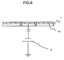
- the wafer platform 1, as shown in Fig.6, contains the ESC electrode 16 buried therein so that the dc voltage may be applied from the ESC power source 9 to the ESC electrode 16.
- the wafer lift pin 3 When the wafer lift pin 3 is located at a top dead center, the wafer 2 is carried out of the vacuum vessel 8 by a vacuum carrying robot 2 or the like to a given position on the wafer lift pin 3. Then, the wafer lift pin 3 is descended to a bottom dead center, where the wafer is placed on the center of the water placing surface of the wafer platform 1 controlled in a given temperature.
- the reactive gas is fed from the gas inlet 7 at a given flow rate and the ESC power source 9 and the high frequency power source 5 are both operated, when the plasma is generated between the wafer platform 1 and the opposed electrode 10.
- the predetermined RIE treatment is completed.
- the ESC power source 9 is stopped and the reactive gas atmosphere inside the vacuum vessel 8 is replaced with inert gas for reducing or removing the residual absorption caused between the wafer 2 and the wafer platform 1.
- the wafer lift pushes the wafer 2 from the wafer placing surface of the wafer platform 1 to the carrying position, and then the wafer 2 is carried out of the vacuum vessel 8 by the vacuum carrying robot or the like. This is a completion of the series of operations.
- Fig.7 is a flowchart showing an operation executed in stripping the wafer.
- the ESC power source 9 is stopped (step 202). Then, the gas being fed to the vacuum vessel 8 is switched from the reactive gas to the inert gas (step 203). The supply power from the high frequency power source 5 is lowered to the allowable minimum power for generating the plasma (as referred to as de-charging plasma, hereinafter) (step 204). Next, the high frequency power source 5 is stopped (step 205). These series of operations result in lowering a negative self-biased voltage occurring on the wafer 2, thereby suppressing extra etching to a minimum and reducing the residual electrostatic absorption.
- the wafer 2 is naturally stripped off the wafer placing surface and then is moved up to the carrying position (step 209). Further, by grounding the wafer lift pin 3 only in the operation of the apparatus (step 208), without losing the high frequency power applied in the RIE treatment, the residual charges between the rear side of the wafer 2 and the wafer platform 1 are discharged to the grounding side for further reducing the residual absorption.
- the wafer 2 absorbed on the wafer platform 1 is forcibly stripped off the wafer platform by a wafer lift pin located on the center of the wafer platform 1 and a swing cam for lifting up the wafer 2 from the outer peripheral portion of the wafer platform 2 in concert with the pushup action of the wafer lift pin 3 located on the peripheral portion of the wafer platform 1.
- the wafer lift pin 3 or a pressurized gas injecting port is located on the outer peripheral portion of the wafer platform 1 so that the wafer 2 may be stripped off the wafer platform 1 by virtue of small force.
- the wafer 2 is forcibly stripped off the wafer platform 1 without reducing the residual absorption caused between the wafer 2 and the wafer platform 1.
- the wafer 2 on the wafer lift pin 3 is inclined or part of the wafer 2 absorbed on the wafer platform 1 overcomes the residual charges, the wafer 2 may be stripped off the wafer platform 1, when the repulsion may take place so that the repulsion may make the wafer 2 bounced.
- the deposition of the reactive creation serves to insulate the wafer 2 from the wafer lift pin 3, that is, keep the wafer 2 out of the grounding contact with the wafer lift pin 3. As a result, the charges left between the wafer 2 and the wafer platform 1 are disallowed to be discharged, thereby disabling to reduce the residual absorption.
- the in-plane uniformity of the etching portion is made worse. This is because any of the foregoing prior arts is arranged to stop only the ESC power source 9 and generate the de-charging plasma from the high frequency power while the high frequency power source is in operation after the completion of the given etching treatment, for proceeding the overflown etching whose wafer in-plane uniformity is worse by the de-charging plasma.
- the semiconductor wafer chucking device comprises a wafer platform, means for feeding inert gas, means for generating ionized gas, and a half-lifting lift pin, wherein the wafer platform is installed in a vacuum vessel and serves to electrostatically absorb the semiconductor wafer, the inert gas feeding means feeds the inert gas to the vacuum vessel, the ionized gas generating means excites the inert gat in the vacuum vessel and generates the ionized gas for neutralizing the charges charged with the semiconductor wafer and the wafer platform, and the half-lifting lift pin serves to strip part of the semiconductor wafer electrostatically absorbed on the wafer platform off the wafer platform and keep the inert gas ionized by the ionized gas generating means in contact with the rear surface of the semiconductor wafer and the top surface of the wafer platform.
- the method for stripping the semiconductor wafer according to the present invention arranged to de-charge the semiconductor wafer electrostatically absorbed on the wafer platform and then stripping the wafer off the wafer platform comprises the steps of: exciting the inert gas led in the vacuum vessel in which the wafer platform is installed and generating the ionized gas for neutralizing the charges charged on the semiconductor wafer and the wafer platform; and stripping part of the semiconductor wafer off the wafer platform in the atmosphere of the ionized gas and keeping the ionized gas in contact with the rear surface of the semiconductor wafer and the top surface of the wafer platform through the gap between the part of the semiconductor wafer and the wafer platform being stripped from each other, for neutralizing the charges charged on the semiconductor wafer and the wafer platform and de-charging the electrostatic force between the wafer platform and the semiconductor wafer.
- the inert gat when stripping the wafer off the wafer platform, the inert gat is fed in the vacuum vessel.
- the ionized gas generating means keeps the vacuum vessel in the atmosphere of the ionized inert gas.
- the half-lifting lift pin is served to lift up the rear surface of the wafer earlier than the wafer lift pin so that only the part of the outer peripheral portion of the wafer is stripped off the wafer platform 1.
- the gap between the rear surface of the wafer and the wafer platform is exposed to the atmosphere of the ionized inert gas, for neutralizing and coupling the residual charges and thereby reducing the residual absorption.
- the wafer can be easily stripped off the wafer platform only by the operation of the wafer lift pin for lifting up the rear surface of the wafer.
- Fig.1 shows the RIE apparatus provided with the semiconductor wafer chucking device according to the embodiment 1 of the present invention.
- the RIE apparatus shown in Fig.1 is constructed so that a wafer platform 1 is opposed to an opposed electrode 10 in a vacuum vessel 8, the vacuum vessel 8 and the opposed electrode 10 are grounded, and the high frequency power is fed from a high frequency power source 5 to the wafer platform 1.
- the opposed electrode 10 contains pores in which the inert gas from a gas inlet 7 is led, so that the plasma is generated in the vacuum vessel 8. This is the essential part of the RIE apparatus.
- the semiconductor wafer chucking device includes the wafer platform 1 on which the wafer 2 is placed in the grounded vacuum vessel 8, an ESC power source 9 for applying a dc voltage onto the wafer platform 1 for fixing the wafer 2 on the wafer platform 2 by virtue of electrostatic absorption, a wafer lift pin 3 for lifting the wafer 2 up to the carrying position (which is the same level as a wafer inlet 8a of the vacuum vessel 8), a half-lifting lift pin 4 for stripping part of an outer peripheral portion of the wafer 2 off the wafer platform 1 when stripping the wafer, an UV ray applying unit (ionized gas generating means) 6 for applying an UV (Ultraviolet) ray to nearby the rear surface of the half-lifted wafer 2, and a gas injecting port 7 for injecting the inert gas in place of the reactive gas in the vacuum vessel 8.
- an ESC power source 9 for applying a dc voltage onto the wafer platform 1 for fixing the wafer 2 on the wafer platform 2 by virtue of electrostatic
- the inert gas is led in the vacuum vessel 8 through the gas injecting port 7 (step 103), so that the atmosphere of the inert gas is kept in the vacuum vessel 8.
- the UV ray applying unit 6 applies the UV ray to the inside of the vacuum vessel 8 (step 104).
- the inert gas absorbs the energy of the UV ray so that the inert gas is excited and ionized.
- the half-lifting lift pin is served to lift up the wafer 2 from the rear surface of the wafer 2 (step 105).
- the part of the wafer 2 lifted by the half-lifting lift pin 4 is stripped off the wafer platform 1, while the opposite part of the wafer 2 is absorbed on the wafer platform 1 by virtue of the residual absorption left on the outer peripheral portion of the wafer platform 1 (step 106).
- the inert gas ionized by the UV ray has a neutralizing effect on the charges existing on the rear surface of the wafer 2 and the top surface of the wafer platform 1, thereby quickly reducing the residual absorption left on the rear surface of the wafer 2 and the top surface of the wafer platform 1 (step 107).
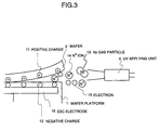
- the de-charging mechanism through the effect of the ionized gas will be supplemented with reference to Fig.3.
- Positive charges 11 exist on the rear surface of the half-lifted part of the wafer 2, while negative charges 12 caused by a negative voltage applied by the ESC electrode 15 exist on the top surface of the wafer platform 1. Those charges are the cause of the residual absorption that is a bottleneck in stripping the wafter.
- the inert gas particles 13 such as N 2 gas are filled in advance between the wafer 2 and the wafer platform 1.
- the UV ray applying unit 6 operates to apply the UV ray to the inert gas particles 13 so that the energy-absorbed N 2 gas particles are excited and thereby separated into N + ions 14 and electrons 15.
- These N + ions 14 are attracted to the negative charges 12 existing on the wafer platform 1 having the opposite polarity and are electrically coupled therewith.
- the electrons 15 are coupled with the positive charges 11, so that both of the electrons 15 and the positive charges 11 are neutralized, which results in removing the residual charges.
- the wafer lift pin 3 is raised (steps 108 and 109), so that the wafer 2 may be easily stripped off the water platform 1 without positional shift or bouncing (step 110).
- the time taken in reducing the residual absorption is as short as one second, which is far shorter than the time taken in activating the de-charging plasma (about five to ten seconds).
- the rate-determining stage of the wafer stripping process never lowers the throughput.
- the wafer may be stripped without the etching process, so the wafer in-plane uniformity in the etching treatment is not made worse.
- Fig.4 is a sectional view showing the RIE apparatus provided with the semiconductor wafer chucking device according to the embodiment 2 of the present invention.
- the embodiment 2 of the present invention is different from the embodiment 1 in that the half-lifting lift pin 4a uses one of the wafer lift pins 3.
- the half-lifting lift pin 4a whose pin tip is higher than the tip of the wafer lift pin 3 is kept in the waiting state under the wafer 2 so that the lift pin 4a is positioned to be faced with the UV ray applying unit 6.
- the half-lifting lift pin 4a is lifted up in advance of the remaining wafer lift pins 3 so that the part of the wafer 2 is stripped.
- the embodiment 2 has the same principle on which the residual absorption between the wafer 2 and the wafer platform 1 as the embodiment 1.
- the operation of the embodiment 2 is basically the same as that of the embodiment 1.
- the wafter lift pins 3 are moved in synchronous to the half-lifting lift pin 4a.
- the height relation between the half-lifting lift pin 4a and the lift pins 3 from the start to the end of the wafer stripping is made constant so that the wafer 2 is inclined after stripping the wafer 2.
- the height of the half-lifting lift pin 4a is higher by about 1 mm than the height of the lift pins 3, so the inclination of the wafer 2 after stripping the wafer 2 is negligible.
- This embodiment 2 is therefore advantageous in that it provides the same performance and the simplified structure.
- the absorption caused by the electrostatics left between the wafer and the wafer platform is removed before stripping the wafer off the wafer platform.
- the present invention does not need a special action for eliminating the wafer, which makes contribution to reducing the time taken in stripping the wafer.
Landscapes
- Container, Conveyance, Adherence, Positioning, Of Wafer (AREA)
- Jigs For Machine Tools (AREA)
- Drying Of Semiconductors (AREA)
- Cleaning Or Drying Semiconductors (AREA)
Applications Claiming Priority (3)
| Application Number | Priority Date | Filing Date | Title |
|---|---|---|---|
| JP7033996A JP3163973B2 (ja) | 1996-03-26 | 1996-03-26 | 半導体ウエハ・チャック装置及び半導体ウエハの剥離方法 |
| JP7033996 | 1996-03-26 | ||
| JP70339/96 | 1996-03-26 |
Publications (2)
| Publication Number | Publication Date |
|---|---|
| EP0798775A2 true EP0798775A2 (de) | 1997-10-01 |
| EP0798775A3 EP0798775A3 (de) | 1999-07-07 |
Family
ID=13428569
Family Applications (1)
| Application Number | Title | Priority Date | Filing Date |
|---|---|---|---|
| EP97105047A Withdrawn EP0798775A3 (de) | 1996-03-26 | 1997-03-25 | Vorrichtung zur Halterung einer Halbleiterscheibe sowie Verfahren zum Entfernen einer Halbleiterscheibe |
Country Status (4)
| Country | Link |
|---|---|
| US (1) | US6174370B1 (de) |
| EP (1) | EP0798775A3 (de) |
| JP (1) | JP3163973B2 (de) |
| KR (1) | KR100298910B1 (de) |
Cited By (8)
| Publication number | Priority date | Publication date | Assignee | Title |
|---|---|---|---|---|
| WO1999066549A1 (en) * | 1998-06-16 | 1999-12-23 | Surface Technology Systems Limited | Method and apparatus for dechucking a substrate from an electrostatic chuck |
| US6056825A (en) * | 1997-06-18 | 2000-05-02 | Sez Semiconductor-Equipment Zubehor Fur Die Halbleiterfertigung Ag | Rotary chuck including pins for lifting wafers |
| EP1148541A1 (de) * | 2000-04-19 | 2001-10-24 | Applied Materials, Inc. | Verfahren und Vorrichtung zum Konditionieren eines elektrostatischen Halters |
| EP1202338A1 (de) * | 2000-10-23 | 2002-05-02 | Ngk Insulators, Ltd. | Suzeptor für Halbleiterherstellungsgeräte |
| SG90780A1 (en) * | 2000-07-20 | 2002-08-20 | Applied Materials Inc | Method and apparatus for dechucking a substrate |
| WO2010068268A1 (en) * | 2008-12-10 | 2010-06-17 | Axcelis Technologies, Inc | De-clamping wafers from an electrostatic chuck |
| TWI566306B (zh) * | 2012-01-19 | 2017-01-11 | Asahi Glass Co Ltd | A peeling device and a method for manufacturing the electronic component |
| WO2019197128A3 (en) * | 2018-04-12 | 2019-11-21 | Asml Netherlands B.V. | Apparatus comprising an electrostatic clamp and method for operating the apparatus |
Families Citing this family (19)
| Publication number | Priority date | Publication date | Assignee | Title |
|---|---|---|---|---|
| US6125025A (en) * | 1998-09-30 | 2000-09-26 | Lam Research Corporation | Electrostatic dechucking method and apparatus for dielectric workpieces in vacuum processors |
| US6364958B1 (en) * | 2000-05-24 | 2002-04-02 | Applied Materials, Inc. | Plasma assisted semiconductor substrate processing chamber having a plurality of ground path bridges |
| US6528435B1 (en) * | 2000-08-25 | 2003-03-04 | Wafermasters, Inc. | Plasma processing |
| DE10196643B4 (de) * | 2001-07-23 | 2008-12-11 | Mitsubishi Denki K.K. | Herstellungsverfahren für einen Dünnschicht-Strukturkörper |
| US6864563B1 (en) * | 2002-05-30 | 2005-03-08 | Lsi Logic Corporation | Grounding mechanism for semiconductor devices |
| JP4372443B2 (ja) * | 2003-04-01 | 2009-11-25 | 東京エレクトロン株式会社 | 処理装置および処理方法 |
| US8033245B2 (en) * | 2004-02-12 | 2011-10-11 | Applied Materials, Inc. | Substrate support bushing |
| US7597816B2 (en) * | 2004-09-03 | 2009-10-06 | Lam Research Corporation | Wafer bevel polymer removal |
| JP2010199239A (ja) * | 2009-02-24 | 2010-09-09 | Tokyo Electron Ltd | 被処理基板の除電方法及び基板処理装置 |
| US8888086B2 (en) * | 2011-05-11 | 2014-11-18 | Sematech, Inc. | Apparatus with surface protector to inhibit contamination |
| JP2014072272A (ja) * | 2012-09-28 | 2014-04-21 | Toppan Printing Co Ltd | プラズマエッチング方法およびプラズマエッチング装置 |
| US9232626B2 (en) | 2013-11-04 | 2016-01-05 | Kla-Tencor Corporation | Wafer grounding using localized plasma source |
| JP2018006392A (ja) | 2016-06-28 | 2018-01-11 | ルネサスエレクトロニクス株式会社 | 半導体装置の製造方法 |
| TWI671844B (zh) | 2017-01-30 | 2019-09-11 | 日商新川股份有限公司 | 拾取裝置以及拾取方法 |
| KR102322767B1 (ko) * | 2017-03-10 | 2021-11-08 | 삼성디스플레이 주식회사 | 기판과 스테이지 간의 분리 기구가 개선된 기판 처리 장치 및 그것을 이용한 기판 처리 방법 |
| JP6948822B2 (ja) | 2017-04-25 | 2021-10-13 | 東京エレクトロン株式会社 | 基板処理装置及び基板取り外し方法 |
| JP7120833B2 (ja) * | 2018-07-10 | 2022-08-17 | Jswアクティナシステム株式会社 | レーザ処理装置 |
| EP3899665A1 (de) * | 2018-12-20 | 2021-10-27 | ASML Netherlands B.V. | Objekttisch mit einer elektrostatischen klemme |
| JP7265430B2 (ja) * | 2019-07-02 | 2023-04-26 | 株式会社ディスコ | 処理装置 |
Family Cites Families (22)
| Publication number | Priority date | Publication date | Assignee | Title |
|---|---|---|---|---|
| JPS59135730A (ja) * | 1983-01-24 | 1984-08-04 | Hitachi Ltd | 表面改質装置 |
| JPH02159744A (ja) * | 1988-12-14 | 1990-06-19 | Fuji Electric Co Ltd | 半導体ウエハチャック装置のウエハ離脱機構 |
| JPH07109855B2 (ja) | 1990-02-14 | 1995-11-22 | 株式会社日立製作所 | 静電チャックの帯電除去方法 |
| JP2635195B2 (ja) | 1990-02-19 | 1997-07-30 | 株式会社日立製作所 | 静電チャックの帯電除去方法 |
| JP2506219B2 (ja) * | 1990-06-19 | 1996-06-12 | 富士通株式会社 | 静電吸着方法 |
| JPH04271286A (ja) | 1991-02-22 | 1992-09-28 | Fujitsu Ltd | 静電チャック |
| JP3182615B2 (ja) * | 1991-04-15 | 2001-07-03 | アネルバ株式会社 | プラズマ処理方法および装置 |
| US5539609A (en) * | 1992-12-02 | 1996-07-23 | Applied Materials, Inc. | Electrostatic chuck usable in high density plasma |
| US5310453A (en) * | 1992-02-13 | 1994-05-10 | Tokyo Electron Yamanashi Limited | Plasma process method using an electrostatic chuck |
| JP3259380B2 (ja) * | 1992-12-04 | 2002-02-25 | ソニー株式会社 | 半導体装置の製造方法 |
| JPH06177078A (ja) * | 1992-12-08 | 1994-06-24 | Tokyo Electron Ltd | 静電チャック |
| JPH06188305A (ja) * | 1992-12-17 | 1994-07-08 | Tokyo Electron Ltd | 被吸着体の離脱装置および被吸着体の離脱方法およびプラズマ処理装置 |
| JP3315197B2 (ja) * | 1993-05-17 | 2002-08-19 | 東京エレクトロン株式会社 | プラズマ処理方法 |
| US5557215A (en) * | 1993-05-12 | 1996-09-17 | Tokyo Electron Limited | Self-bias measuring method, apparatus thereof and electrostatic chucking apparatus |
| TW255839B (de) * | 1993-05-20 | 1995-09-01 | Hitachi Seisakusyo Kk | |
| US5380566A (en) * | 1993-06-21 | 1995-01-10 | Applied Materials, Inc. | Method of limiting sticking of body to susceptor in a deposition treatment |
| JP3671379B2 (ja) * | 1994-02-03 | 2005-07-13 | アネルバ株式会社 | 静電吸着された被処理基板の離脱機構を持つプラズマ処理装置および静電吸着された被処理基板の離脱方法 |
| TW288253B (de) * | 1994-02-03 | 1996-10-11 | Aneruba Kk | |
| JP3082624B2 (ja) * | 1994-12-28 | 2000-08-28 | 住友金属工業株式会社 | 静電チャックの使用方法 |
| JP3005461B2 (ja) * | 1995-11-24 | 2000-01-31 | 日本電気株式会社 | 静電チャック |
| US5793192A (en) * | 1996-06-28 | 1998-08-11 | Lam Research Corporation | Methods and apparatuses for clamping and declamping a semiconductor wafer in a wafer processing system |
| TW334609B (en) * | 1996-09-19 | 1998-06-21 | Hitachi Ltd | Electrostatic chuck, method and device for processing sanyle use the same |
-
1996
- 1996-03-26 JP JP7033996A patent/JP3163973B2/ja not_active Expired - Fee Related
-
1997
- 1997-03-25 EP EP97105047A patent/EP0798775A3/de not_active Withdrawn
- 1997-03-26 US US08/827,312 patent/US6174370B1/en not_active Expired - Fee Related
- 1997-03-26 KR KR1019970010581A patent/KR100298910B1/ko not_active Expired - Fee Related
Cited By (12)
| Publication number | Priority date | Publication date | Assignee | Title |
|---|---|---|---|---|
| US6056825A (en) * | 1997-06-18 | 2000-05-02 | Sez Semiconductor-Equipment Zubehor Fur Die Halbleiterfertigung Ag | Rotary chuck including pins for lifting wafers |
| US6316367B1 (en) | 1997-06-18 | 2001-11-13 | Sez Semiconductor-Equipment Zubehor | Process and device for handling disk-like objects, especially silicon wafers |
| WO1999066549A1 (en) * | 1998-06-16 | 1999-12-23 | Surface Technology Systems Limited | Method and apparatus for dechucking a substrate from an electrostatic chuck |
| EP1148541A1 (de) * | 2000-04-19 | 2001-10-24 | Applied Materials, Inc. | Verfahren und Vorrichtung zum Konditionieren eines elektrostatischen Halters |
| SG90780A1 (en) * | 2000-07-20 | 2002-08-20 | Applied Materials Inc | Method and apparatus for dechucking a substrate |
| US6676761B2 (en) | 2000-07-20 | 2004-01-13 | Applied Materials, Inc. | Method and apparatus for dechucking a substrate |
| US7160392B2 (en) | 2000-07-20 | 2007-01-09 | Applied Materials, Inc. | Method for dechucking a substrate |
| EP1202338A1 (de) * | 2000-10-23 | 2002-05-02 | Ngk Insulators, Ltd. | Suzeptor für Halbleiterherstellungsgeräte |
| US6645304B2 (en) | 2000-10-23 | 2003-11-11 | Ngk Insulators, Ltd. | Susceptors for semiconductor-producing apparatuses |
| WO2010068268A1 (en) * | 2008-12-10 | 2010-06-17 | Axcelis Technologies, Inc | De-clamping wafers from an electrostatic chuck |
| TWI566306B (zh) * | 2012-01-19 | 2017-01-11 | Asahi Glass Co Ltd | A peeling device and a method for manufacturing the electronic component |
| WO2019197128A3 (en) * | 2018-04-12 | 2019-11-21 | Asml Netherlands B.V. | Apparatus comprising an electrostatic clamp and method for operating the apparatus |
Also Published As
| Publication number | Publication date |
|---|---|
| JPH09260475A (ja) | 1997-10-03 |
| KR100298910B1 (ko) | 2001-10-19 |
| JP3163973B2 (ja) | 2001-05-08 |
| US6174370B1 (en) | 2001-01-16 |
| EP0798775A3 (de) | 1999-07-07 |
| KR970067549A (ko) | 1997-10-13 |
Similar Documents
| Publication | Publication Date | Title |
|---|---|---|
| US6174370B1 (en) | Semiconductor wafer chucking device and method for stripping semiconductor wafer | |
| EP0720217B1 (de) | Elektrostatischer Halter | |
| JP4013753B2 (ja) | 半導体ウェハの切断方法 | |
| US7258811B2 (en) | Wafer stage including electrostatic chuck and method for dechucking wafer using the wafer stage | |
| US20020179577A1 (en) | Plasma processing method and apparatus for eliminating damages in a plasma process of a substrate | |
| CN1669109A (zh) | 等离子体处理设备和等离子体处理方法 | |
| JPH0831449B2 (ja) | 閉込められたプラズマエッチングを使用する材料除去装置 | |
| JP2004047511A (ja) | 離脱方法、処理方法、静電吸着装置および処理装置 | |
| JPH09120988A (ja) | プラズマ処理方法 | |
| JPH07263531A (ja) | 静電吸着された被処理基板の離脱機構を持つプラズマ処理装置および静電吸着された被処理基板の離脱方法 | |
| KR100304981B1 (ko) | 웨이퍼 표면의 잔류 전하 제거 방법 | |
| JP3778959B2 (ja) | 基板処理装置 | |
| JP3162272B2 (ja) | プラズマ処理方法 | |
| JP3315197B2 (ja) | プラズマ処理方法 | |
| US12521773B2 (en) | Method of cleaning electrostatic chuck and method of manufacturing semiconductor device while exposing electrostatic chuck to plasma and introducing electron current | |
| JP3027781B2 (ja) | プラズマ処理方法 | |
| JP3118497B2 (ja) | プラズマ処理装置及びプラズマ処理方法 | |
| JP2002367967A (ja) | プラズマ処理方法及びその装置 | |
| JPH11111830A (ja) | 静電吸着装置および静電吸着方法、ならびにそれを用いた処理装置および処理方法 | |
| JP2985761B2 (ja) | 試料処理方法 | |
| JPH1131661A (ja) | 半導体ウエハ成膜装置 | |
| JP2006135081A (ja) | 基板処理方法及び基板処理装置 | |
| JP2976898B2 (ja) | ドライエッチング方法 | |
| JP2002043285A (ja) | 半導体装置の製造方法及びプラズマエッチング装置 | |
| JPH05279876A (ja) | ドライエッチング方法 |
Legal Events
| Date | Code | Title | Description |
|---|---|---|---|
| PUAI | Public reference made under article 153(3) epc to a published international application that has entered the european phase |
Free format text: ORIGINAL CODE: 0009012 |
|
| AK | Designated contracting states |
Kind code of ref document: A2 Designated state(s): DE FR GB |
|
| PUAL | Search report despatched |
Free format text: ORIGINAL CODE: 0009013 |
|
| AK | Designated contracting states |
Kind code of ref document: A3 Designated state(s): DE FR GB |
|
| 17P | Request for examination filed |
Effective date: 19990531 |
|
| 17Q | First examination report despatched |
Effective date: 20030711 |
|
| STAA | Information on the status of an ep patent application or granted ep patent |
Free format text: STATUS: THE APPLICATION HAS BEEN WITHDRAWN |
|
| 18W | Application withdrawn |
Effective date: 20030820 |