EP0800136A1 - Source de signal d'horloge à tolerance de fautes pour un système tripliqué de traitement de données - Google Patents
Source de signal d'horloge à tolerance de fautes pour un système tripliqué de traitement de données Download PDFInfo
- Publication number
- EP0800136A1 EP0800136A1 EP97104840A EP97104840A EP0800136A1 EP 0800136 A1 EP0800136 A1 EP 0800136A1 EP 97104840 A EP97104840 A EP 97104840A EP 97104840 A EP97104840 A EP 97104840A EP 0800136 A1 EP0800136 A1 EP 0800136A1
- Authority
- EP
- European Patent Office
- Prior art keywords
- oscillator
- clock
- master
- data processing
- slave
- Prior art date
- Legal status (The legal status is an assumption and is not a legal conclusion. Google has not performed a legal analysis and makes no representation as to the accuracy of the status listed.)
- Granted
Links
Images
Classifications
-
- G—PHYSICS
- G06—COMPUTING OR CALCULATING; COUNTING
- G06F—ELECTRIC DIGITAL DATA PROCESSING
- G06F11/00—Error detection; Error correction; Monitoring
- G06F11/07—Responding to the occurrence of a fault, e.g. fault tolerance
- G06F11/16—Error detection or correction of the data by redundancy in hardware
- G06F11/1604—Error detection or correction of the data by redundancy in hardware where the fault affects the clock signals of a processing unit and the redundancy is at or within the level of clock signal generation hardware
-
- H—ELECTRICITY
- H03—ELECTRONIC CIRCUITRY
- H03K—PULSE TECHNIQUE
- H03K17/00—Electronic switching or gating, i.e. not by contact-making and –breaking
-
- G—PHYSICS
- G06—COMPUTING OR CALCULATING; COUNTING
- G06F—ELECTRIC DIGITAL DATA PROCESSING
- G06F1/00—Details not covered by groups G06F3/00 - G06F13/00 and G06F21/00
- G06F1/04—Generating or distributing clock signals or signals derived directly therefrom
-
- G—PHYSICS
- G06—COMPUTING OR CALCULATING; COUNTING
- G06F—ELECTRIC DIGITAL DATA PROCESSING
- G06F1/00—Details not covered by groups G06F3/00 - G06F13/00 and G06F21/00
- G06F1/04—Generating or distributing clock signals or signals derived directly therefrom
- G06F1/10—Distribution of clock signals, e.g. skew
-
- G—PHYSICS
- G06—COMPUTING OR CALCULATING; COUNTING
- G06F—ELECTRIC DIGITAL DATA PROCESSING
- G06F11/00—Error detection; Error correction; Monitoring
- G06F11/07—Responding to the occurrence of a fault, e.g. fault tolerance
- G06F11/16—Error detection or correction of the data by redundancy in hardware
- G06F11/18—Error detection or correction of the data by redundancy in hardware using passive fault-masking of the redundant circuits
- G06F11/183—Error detection or correction of the data by redundancy in hardware using passive fault-masking of the redundant circuits by voting, the voting not being performed by the redundant components
Definitions
- the present invention relates to fault tolerant data processing systems.
- Data processing systems require a source of clock signals to synchronise the individual processing steps that occur within them. For example, if an arithmetic unit is to be used to sum the values stored in two memory locations and then to store the result in a further memory location, the individual steps required would be first to transfer the values to be summed from memory into the input registers of the arithmetic unit, to retrieve the values from the input registers and operate on them in the arithmetic unit, to transfer the result of the operation to an output register and then to transfer the result from the output register to memory. These steps must be carried out sequentially and clock signals are needed to ensure correct synchronisation of these various steps.
- the present invention therefore seeks to provide a source of clock signals for supplying stable clock signals to three independent processing sub-systems in which the source is itself fault tolerant and can supply independently generated and correctly synchronised clock pulses to the three processing sub-systems.
- a clock signal source for providing three mutually independent clock signals to three processing sub-systems of a triplicated data processing system, the source comprising a master reference oscillator, a slave reference oscillator phase locked to the master oscillator but capable of operating as an independent oscillator in the event of failure of the main reference oscillator, and three mutually independent clock circuits each connected to the master and slave reference oscillators each clock circuit being capable of detecting malfunction of the reference oscillators and being phase locked to the output signal of the master reference oscillator when both master and slave reference oscillators are functional, and being phase locked to either one of the reference oscillators when a malfunction is detected in the other.
- the slave reference oscillator should develop a fault, then a warning is issued by the clock circuits that a fault has been detected but the clock circuits continue in synchronous operation because they each remain in phase with the master reference oscillator.
- the slave reference oscillator will cease to be phase locked to it but the slave reference oscillator will nevertheless continue to function independently.
- Each clock circuit will now be phase locked to the slave reference oscillator and will issue a warning of failure of the master reference oscillator.
- each clock circuit should itself include a local oscillator.
- a comparison between the output signal of the local oscillator and the two reference oscillators will indicate if one of the reference oscillators is not oscillating or oscillating at an overtone of the correct frequency, these being the two common failure modes of the reference oscillators.
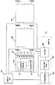
- the clock signal source in the drawing comprises a master reference oscillator 10 which is formed as a stable crystal oscillator supplying the same reference signal to four separate outputs through respective separate buffer amplifiers (not shown).
- the buffer amplifiers ensure that there is no interaction between any circuits connected to the outputs of the master reference oscillator 10.
- a first of the four outputs of the master reference oscillator 10 is applied to a reference slave oscillator 12.
- the reference slave oscillator 12 comprises a voltage controlled crystal oscillator 12a the output signal of which is compared in phase with the input signal that is received from the master reference oscillator 10 by a comparator 12b.
- the output of the comparator 12b is fed through a low pass filter 12c to the voltage controlled oscillator 12a, the closed negative feedback phase locked loop ensuring that the oscillator 12a is controlled to remain in phase with the master reference oscillator 10 at all times.
- phase comparator 12b If the phase comparator 12b should fail to receive a signal from the master reference oscillator 10, then the voltage controlled oscillator 12a will receive a steady d.c. voltage maintaining its frequency at the nominal frequency of the slave reference oscillator 12a.
- the output of the slave reference oscillator 12 is applied through three separate buffer amplifiers to three clock circuits 14a, 14b and 14c.
- Each of the clock circuits 14a to 14c thus receives two reference input signals, one from the master reference oscillator 10 and the other from the slave reference oscillator 12. In the absence of a fault, these two clock signals from the master and slave reference oscillators should both be present and in synchronism with one another. If the slave reference oscillator 12 should fail, then each slave oscillator 14a to 14c will receive only the clock signal from the master reference oscillator 10 and conversely if the master reference oscillator 10 should fail, then the slave reference oscillator 12 will produce a clock signal of the same nominal frequency.
- the clock circuit 14a which is constructed in the same way as the other two clock circuits 14b and 14c, has a control circuit 16 connected to receive the master and slave reference signals and also to a further local crystal oscillator 18.
- the local oscillator 18 is used by the control circuit 16 only for the purpose of determining if a fault has developed in the master or slave reference oscillators 10 and 12.
- the three possible states for each of these reference oscillators 10 and 12 are first, that it is oscillating at the correct frequency, second, that it is not oscillating at all, and third, that it is oscillating at an overtone or harmonic of the correct frequency.
- a fault in one or both of the reference oscillators 10 and 12 will be separately indicated by each of the clock circuits.
- failure in any part of only one of the clock circuits 14a to 14c will affect only that clock circuit. This allows warnings from the clock circuits 14a to 14c of faults in the reference oscillators 10 and 12 to be disregarded unless then are in mutual agreement.
- the output of the control circuit 16 is applied to a clock driver circuit 20 which generates the various clock signals ClkA1-ClkAn required by the data processing sub-system associated with the slave clock circuit 14a.
- the driver circuit 20 may comprise a frequency divider to produce a lower clock frequency at one of the output terminals, if such is required. If a higher frequency than the master reference frequency is required, then the clock driver circuit 22 may comprise an oscillator, a frequency divider and a phase locked loop, the oscillator being locked onto a multiple of the frequency of the signal received from the control circuit 16 by comparing the phase of its frequency divided output with the signal from the control circuit 16 in the phase locked loop. In this way, each clock driver circuit independently generates the various clock signals ClkA1 to CLkCn that are required by its associated data processing sub-system.
- the invention provides three mutually independent sources of clock signals that are nevertheless always in phase with one another because they are all separately synchronised with an external reference. Furthermore, the data processing system is tolerant to a fault occurring anywhere in the clock source, including the external reference, because the external reference is itself duplicated and there is automatic switching to the slave or stand-by reference in the event of a detected failure.
Landscapes
- Engineering & Computer Science (AREA)
- Theoretical Computer Science (AREA)
- Physics & Mathematics (AREA)
- General Engineering & Computer Science (AREA)
- General Physics & Mathematics (AREA)
- Quality & Reliability (AREA)
- Stabilization Of Oscillater, Synchronisation, Frequency Synthesizers (AREA)
- Hardware Redundancy (AREA)
- Synchronisation In Digital Transmission Systems (AREA)
Applications Claiming Priority (2)
| Application Number | Priority Date | Filing Date | Title |
|---|---|---|---|
| GB9607093 | 1996-04-03 | ||
| GB9607093A GB2311881B (en) | 1996-04-03 | 1996-04-03 | Fault tolerant data processing systems |
Publications (2)
| Publication Number | Publication Date |
|---|---|
| EP0800136A1 true EP0800136A1 (fr) | 1997-10-08 |
| EP0800136B1 EP0800136B1 (fr) | 2001-08-22 |
Family
ID=10791590
Family Applications (1)
| Application Number | Title | Priority Date | Filing Date |
|---|---|---|---|
| EP97104840A Expired - Lifetime EP0800136B1 (fr) | 1996-04-03 | 1997-03-21 | Source de signal d'horloge à tolerance de fautes pour un système tripliqué de traitement de données |
Country Status (7)
| Country | Link |
|---|---|
| US (1) | US5859996A (fr) |
| EP (1) | EP0800136B1 (fr) |
| KR (1) | KR100437289B1 (fr) |
| CN (1) | CN1130634C (fr) |
| DE (1) | DE69706215T2 (fr) |
| GB (1) | GB2311881B (fr) |
| SG (1) | SG50811A1 (fr) |
Families Citing this family (4)
| Publication number | Priority date | Publication date | Assignee | Title |
|---|---|---|---|---|
| SE9702176L (sv) * | 1997-06-06 | 1998-12-07 | Ericsson Telefon Ab L M | En maskinvarukonstruktion för majoritetsval, samt test och underhåll av majoritetsval |
| US6188286B1 (en) | 1999-03-30 | 2001-02-13 | Infineon Technologies North America Corp. | Method and system for synchronizing multiple subsystems using one voltage-controlled oscillator |
| US6970045B1 (en) | 2003-06-25 | 2005-11-29 | Nel Frequency Controls, Inc. | Redundant clock module |
| CN101047490B (zh) * | 2006-05-11 | 2011-07-20 | 华为技术有限公司 | 一种通信系统时间故障的检测方法及其装置 |
Citations (3)
| Publication number | Priority date | Publication date | Assignee | Title |
|---|---|---|---|---|
| US4282493A (en) * | 1979-07-02 | 1981-08-04 | Motorola, Inc. | Redundant clock signal generating circuitry |
| US4644498A (en) * | 1983-04-04 | 1987-02-17 | General Electric Company | Fault-tolerant real time clock |
| EP0365819A2 (fr) * | 1988-10-25 | 1990-05-02 | International Business Machines Corporation | Horloges synchronisées tolérant les fautes pour systèmes à multiprocesseurs |
Family Cites Families (5)
| Publication number | Priority date | Publication date | Assignee | Title |
|---|---|---|---|---|
| US4185245A (en) * | 1978-05-15 | 1980-01-22 | International Telephone And Telegraph Corporation | Fault-tolerant clock signal distribution arrangement |
| US4920540A (en) * | 1987-02-25 | 1990-04-24 | Stratus Computer, Inc. | Fault-tolerant digital timing apparatus and method |
| US5133064A (en) * | 1987-04-27 | 1992-07-21 | Hitachi, Ltd. | Data processing system generating clock signal from an input clock, phase locked to the input clock and used for clocking logic devices |
| US5355090A (en) * | 1989-10-06 | 1994-10-11 | Rockwell International Corporation | Phase corrector for redundant clock systems and method |
| US5371764A (en) * | 1992-06-26 | 1994-12-06 | International Business Machines Corporation | Method and apparatus for providing an uninterrupted clock signal in a data processing system |
-
1996
- 1996-04-03 GB GB9607093A patent/GB2311881B/en not_active Expired - Fee Related
-
1997
- 1997-03-21 EP EP97104840A patent/EP0800136B1/fr not_active Expired - Lifetime
- 1997-03-21 DE DE69706215T patent/DE69706215T2/de not_active Expired - Lifetime
- 1997-03-26 SG SG1997000979A patent/SG50811A1/en unknown
- 1997-03-26 US US08/824,283 patent/US5859996A/en not_active Expired - Lifetime
- 1997-04-01 KR KR1019970011965A patent/KR100437289B1/ko not_active Expired - Fee Related
- 1997-04-03 CN CN97109588A patent/CN1130634C/zh not_active Expired - Fee Related
Patent Citations (3)
| Publication number | Priority date | Publication date | Assignee | Title |
|---|---|---|---|---|
| US4282493A (en) * | 1979-07-02 | 1981-08-04 | Motorola, Inc. | Redundant clock signal generating circuitry |
| US4644498A (en) * | 1983-04-04 | 1987-02-17 | General Electric Company | Fault-tolerant real time clock |
| EP0365819A2 (fr) * | 1988-10-25 | 1990-05-02 | International Business Machines Corporation | Horloges synchronisées tolérant les fautes pour systèmes à multiprocesseurs |
Also Published As
| Publication number | Publication date |
|---|---|
| KR970072677A (ko) | 1997-11-07 |
| GB2311881B (en) | 2000-03-29 |
| CN1130634C (zh) | 2003-12-10 |
| DE69706215D1 (de) | 2001-09-27 |
| SG50811A1 (en) | 1998-07-20 |
| GB2311881A (en) | 1997-10-08 |
| EP0800136B1 (fr) | 2001-08-22 |
| CN1175131A (zh) | 1998-03-04 |
| KR100437289B1 (ko) | 2004-09-13 |
| GB9607093D0 (en) | 1996-06-05 |
| US5859996A (en) | 1999-01-12 |
| DE69706215T2 (de) | 2002-05-16 |
| GB2311881A8 (en) | 1998-02-12 |
Similar Documents
| Publication | Publication Date | Title |
|---|---|---|
| US4683570A (en) | Self-checking digital fault detector for modular redundant real time clock | |
| US6516422B1 (en) | Computer system including multiple clock sources and failover switching | |
| US5422915A (en) | Fault tolerant clock distribution system | |
| US4979191A (en) | Autonomous N-modular redundant fault tolerant clock system | |
| EP1262022A2 (fr) | Systeme et procede de boucle a phase asservie | |
| EP1476800B1 (fr) | Signaux d'horloge continus | |
| EP0800136B1 (fr) | Source de signal d'horloge à tolerance de fautes pour un système tripliqué de traitement de données | |
| KR100237545B1 (ko) | 시디엠에이 시스템의 이중화 시간/주파수 발생장치 | |
| JP2543138B2 (ja) | 網同期装置および網同期方法 | |
| US6999546B2 (en) | System and method for timing references for line interfaces | |
| KR100406863B1 (ko) | 다중컴퓨터 시스템의 클럭 생성장치 | |
| JPH06232739A (ja) | クロック冗長化方式 | |
| JP2518909B2 (ja) | クロック発生回路の二重化方式 | |
| JPH0347615B2 (fr) | ||
| KR200185362Y1 (ko) | 시스템 클럭 이중화 장치 | |
| KR0180669B1 (ko) | 전전자 교환기 망동기 장치 | |
| US7468991B2 (en) | Methods and devices for synchronizing the timing of logic cards in a packet switching system without data loss | |
| JPH0457536A (ja) | クロック供給方式 | |
| JP3327018B2 (ja) | クロック供給装置 | |
| KR100328761B1 (ko) | 광통신 시스템의 시스템 클럭 유니트 스위칭 장치 | |
| JPH0662481A (ja) | ディジタル交換機の同期信号発生回路 | |
| JPH04257931A (ja) | 計算機システム | |
| JPH03136116A (ja) | クロツク供給装置 | |
| JPS61267493A (ja) | クロツク供給装置 | |
| JPH0427229A (ja) | 伝送装置 |
Legal Events
| Date | Code | Title | Description |
|---|---|---|---|
| PUAI | Public reference made under article 153(3) epc to a published international application that has entered the european phase |
Free format text: ORIGINAL CODE: 0009012 |
|
| AK | Designated contracting states |
Kind code of ref document: A1 Designated state(s): DE FR GB IT |
|
| 17P | Request for examination filed |
Effective date: 19980331 |
|
| 17Q | First examination report despatched |
Effective date: 20000204 |
|
| GRAG | Despatch of communication of intention to grant |
Free format text: ORIGINAL CODE: EPIDOS AGRA |
|
| GRAG | Despatch of communication of intention to grant |
Free format text: ORIGINAL CODE: EPIDOS AGRA |
|
| GRAH | Despatch of communication of intention to grant a patent |
Free format text: ORIGINAL CODE: EPIDOS IGRA |
|
| GRAH | Despatch of communication of intention to grant a patent |
Free format text: ORIGINAL CODE: EPIDOS IGRA |
|
| GRAA | (expected) grant |
Free format text: ORIGINAL CODE: 0009210 |
|
| AK | Designated contracting states |
Kind code of ref document: B1 Designated state(s): DE FR GB IT |
|
| RIN1 | Information on inventor provided before grant (corrected) |
Inventor name: RABI-LALEH, ESMAEEL Inventor name: DRYER, MICHAEL DAVID |
|
| REF | Corresponds to: |
Ref document number: 69706215 Country of ref document: DE Date of ref document: 20010927 |
|
| REG | Reference to a national code |
Ref country code: GB Ref legal event code: IF02 |
|
| ET | Fr: translation filed | ||
| PG25 | Lapsed in a contracting state [announced via postgrant information from national office to epo] |
Ref country code: GB Free format text: LAPSE BECAUSE OF NON-PAYMENT OF DUE FEES Effective date: 20020321 |
|
| PLBE | No opposition filed within time limit |
Free format text: ORIGINAL CODE: 0009261 |
|
| STAA | Information on the status of an ep patent application or granted ep patent |
Free format text: STATUS: NO OPPOSITION FILED WITHIN TIME LIMIT |
|
| 26N | No opposition filed | ||
| GBPC | Gb: european patent ceased through non-payment of renewal fee |
Effective date: 20020321 |
|
| REG | Reference to a national code |
Ref country code: GB Ref legal event code: 727A |
|
| REG | Reference to a national code |
Ref country code: GB Ref legal event code: 727H |
|
| REG | Reference to a national code |
Ref country code: FR Ref legal event code: CD |
|
| REG | Reference to a national code |
Ref country code: DE Ref legal event code: R082 Ref document number: 69706215 Country of ref document: DE Representative=s name: BARDEHLE PAGENBERG PARTNERSCHAFT PATENTANWAELT, DE |
|
| REG | Reference to a national code |
Ref country code: DE Ref legal event code: R082 Ref document number: 69706215 Country of ref document: DE Representative=s name: GRUENECKER PATENT- UND RECHTSANWAELTE PARTG MB, DE Effective date: 20130211 Ref country code: DE Ref legal event code: R082 Ref document number: 69706215 Country of ref document: DE Representative=s name: MAIKOWSKI & NINNEMANN PATENTANWAELTE, DE Effective date: 20130211 Ref country code: DE Ref legal event code: R082 Ref document number: 69706215 Country of ref document: DE Representative=s name: BARDEHLE PAGENBERG PARTNERSCHAFT PATENTANWAELT, DE Effective date: 20130211 Ref country code: DE Ref legal event code: R081 Ref document number: 69706215 Country of ref document: DE Owner name: ROCKWELL AUTOMATION LTD., MILTON KEYNES, GB Free format text: FORMER OWNER: ICS TRIPLEX TECHNOLOGY LTD., MALDON, ESSEX, GB Effective date: 20130211 Ref country code: DE Ref legal event code: R081 Ref document number: 69706215 Country of ref document: DE Owner name: ROCKWELL AUTOMATION LTD., GB Free format text: FORMER OWNER: ICS TRIPLEX TECHNOLOGY LTD., MALDON, GB Effective date: 20130211 Ref country code: DE Ref legal event code: R081 Ref document number: 69706215 Country of ref document: DE Owner name: ICS TRIPLEX (EMEA) PLC, GB Free format text: FORMER OWNER: ICS TRIPLEX TECHNOLOGY LTD., MALDON, GB Effective date: 20130211 |
|
| REG | Reference to a national code |
Ref country code: DE Ref legal event code: R082 Ref document number: 69706215 Country of ref document: DE Representative=s name: MAIKOWSKI & NINNEMANN PATENTANWAELTE, DE |
|
| REG | Reference to a national code |
Ref country code: DE Ref legal event code: R082 Ref document number: 69706215 Country of ref document: DE Representative=s name: MAIKOWSKI & NINNEMANN PATENTANWAELTE, DE |
|
| REG | Reference to a national code |
Ref country code: DE Ref legal event code: R082 Ref document number: 69706215 Country of ref document: DE Representative=s name: GRUENECKER PATENT- UND RECHTSANWAELTE PARTG MB, DE Effective date: 20130904 Ref country code: DE Ref legal event code: R082 Ref document number: 69706215 Country of ref document: DE Representative=s name: GRUENECKER PATENT- UND RECHTSANWAELTE PARTG MB, DE Effective date: 20130527 Ref country code: DE Ref legal event code: R082 Ref document number: 69706215 Country of ref document: DE Representative=s name: MAIKOWSKI & NINNEMANN PATENTANWAELTE, DE Effective date: 20130904 Ref country code: DE Ref legal event code: R082 Ref document number: 69706215 Country of ref document: DE Representative=s name: MAIKOWSKI & NINNEMANN PATENTANWAELTE, DE Effective date: 20130527 Ref country code: DE Ref legal event code: R081 Ref document number: 69706215 Country of ref document: DE Owner name: ROCKWELL AUTOMATION LTD., MILTON KEYNES, GB Free format text: FORMER OWNER: ICS TRIPLEX (EMEA) PLC, MALDON, ESSEX, GB Effective date: 20130904 Ref country code: DE Ref legal event code: R081 Ref document number: 69706215 Country of ref document: DE Owner name: ROCKWELL AUTOMATION LTD., GB Free format text: FORMER OWNER: ICS TRIPLEX (EMEA) PLC, MALDON, GB Effective date: 20130904 |
|
| REG | Reference to a national code |
Ref country code: FR Ref legal event code: PLFP Year of fee payment: 19 |
|
| REG | Reference to a national code |
Ref country code: DE Ref legal event code: R082 Ref document number: 69706215 Country of ref document: DE Representative=s name: GRUENECKER PATENT- UND RECHTSANWAELTE PARTG MB, DE |
|
| REG | Reference to a national code |
Ref country code: DE Ref legal event code: R082 Ref document number: 69706215 Country of ref document: DE Representative=s name: GRUENECKER PATENT- UND RECHTSANWAELTE PARTG MB, DE |
|
| PGFP | Annual fee paid to national office [announced via postgrant information from national office to epo] |
Ref country code: IT Payment date: 20150324 Year of fee payment: 19 Ref country code: DE Payment date: 20150327 Year of fee payment: 19 |
|
| PGFP | Annual fee paid to national office [announced via postgrant information from national office to epo] |
Ref country code: FR Payment date: 20150317 Year of fee payment: 19 |
|
| REG | Reference to a national code |
Ref country code: DE Ref legal event code: R119 Ref document number: 69706215 Country of ref document: DE |
|
| REG | Reference to a national code |
Ref country code: FR Ref legal event code: ST Effective date: 20161130 |
|
| PG25 | Lapsed in a contracting state [announced via postgrant information from national office to epo] |
Ref country code: DE Free format text: LAPSE BECAUSE OF NON-PAYMENT OF DUE FEES Effective date: 20161001 Ref country code: FR Free format text: LAPSE BECAUSE OF NON-PAYMENT OF DUE FEES Effective date: 20160331 |
|
| PG25 | Lapsed in a contracting state [announced via postgrant information from national office to epo] |
Ref country code: IT Free format text: LAPSE BECAUSE OF NON-PAYMENT OF DUE FEES Effective date: 20160321 |