EP0801396A2 - Circuit d'attaque pour ligne de mot - Google Patents
Circuit d'attaque pour ligne de mot Download PDFInfo
- Publication number
- EP0801396A2 EP0801396A2 EP97105748A EP97105748A EP0801396A2 EP 0801396 A2 EP0801396 A2 EP 0801396A2 EP 97105748 A EP97105748 A EP 97105748A EP 97105748 A EP97105748 A EP 97105748A EP 0801396 A2 EP0801396 A2 EP 0801396A2
- Authority
- EP
- European Patent Office
- Prior art keywords
- terminal
- word line
- transistor
- voltage
- driver circuit
- Prior art date
- Legal status (The legal status is an assumption and is not a legal conclusion. Google has not performed a legal analysis and makes no representation as to the accuracy of the status listed.)
- Withdrawn
Links
Images


Classifications
-
- G—PHYSICS
- G11—INFORMATION STORAGE
- G11C—STATIC STORES
- G11C8/00—Arrangements for selecting an address in a digital store
- G11C8/08—Word line control circuits, e.g. drivers, boosters, pull-up circuits, pull-down circuits, precharging circuits, for word lines
-
- G—PHYSICS
- G11—INFORMATION STORAGE
- G11C—STATIC STORES
- G11C11/00—Digital stores characterised by the use of particular electric or magnetic storage elements; Storage elements therefor
- G11C11/21—Digital stores characterised by the use of particular electric or magnetic storage elements; Storage elements therefor using electric elements
- G11C11/34—Digital stores characterised by the use of particular electric or magnetic storage elements; Storage elements therefor using electric elements using semiconductor devices
- G11C11/40—Digital stores characterised by the use of particular electric or magnetic storage elements; Storage elements therefor using electric elements using semiconductor devices using transistors
- G11C11/401—Digital stores characterised by the use of particular electric or magnetic storage elements; Storage elements therefor using electric elements using semiconductor devices using transistors forming cells needing refreshing or charge regeneration, i.e. dynamic cells
- G11C11/4063—Auxiliary circuits, e.g. for addressing, decoding, driving, writing, sensing or timing
- G11C11/407—Auxiliary circuits, e.g. for addressing, decoding, driving, writing, sensing or timing for memory cells of the field-effect type
- G11C11/408—Address circuits
- G11C11/4085—Word line control circuits, e.g. word line drivers, - boosters, - pull-up, - pull-down, - precharge
Definitions
- This invention relates in general to word line drivers in memory integrated circuits, and in particular to a word line driver circuit for a dynamic random access memory (DRAM) circuit to drive a word line above the positive supply voltage with improved drive capability.
- DRAM dynamic random access memory
- Memory integrated circuits typically include a large number of memory cells located at the cross sections of word lines and bit lines.
- a word line is selected in response to externally supplied memory cell address information.
- the bit lines coupled to the selected word line carry the contents of the selected memory cells.
- the selection of a word line in a DRAM typically involves driving an interconnect line with a relatively heavy capacitive loading, from a low logic level of the negative supply voltage Vss, to a logic high voltage level above the positive supply voltage level.
- the gate capacitances for all of the memory cell access transistors coupled to each word line are the main contributors to the large capacitive loading for a word line.
- the circuit driving each word line must therefore be able to drive the heavily loaded line to the required high voltage level at the required speed.
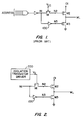
- Figure 1 shows a typical prior art word line driver circuit.
- logic high address inputs at the inputs of an AND gate cause node N1 to be asserted to logic high (or the power supply) voltage Vcc.
- Node N3 is pulled down to logic low (e.g., ground) level by inverter 100, turning off transistor M3.
- Vcc at its gate terminal, transistor M1 is turned on and provides a conductive channel between nodes N1 and N2. This allows the voltage at the gate terminal of the word line driver transistor M2 (node N2) to follow that of node N1 and rise, but only up to a level of Vcc-Vt, where Vt is the threshold voltage for M1.
- a clock signal ⁇ 1 is then applied to the drain terminal of word line driver transistor M2.
- Vcc e.g. 1.5xVcc
- the voltage at node N2 is bootstrapped upwards by the channel capacitance of transistor M2. Accordingly, ignoring the stray capacitances at node N2, the voltage at node N2 may rise to as high as approximately (Vcc-Vt) plus (1.5xVcc).
- transistor M2 is biased on by a gate to source voltage of Vcc-Vt, giving it a certain level of conductivity.
- a transistor threshold voltage (e.g., 0.8v) is a significant percentage of the operating voltage.
- the impact of the loss of a threshold voltage is a lot more severe on the drive capability of the WL driver circuit operating at 3.3v Vcc level than was the case for the same circuit operating at 5.0v Vcc.
- the size of the driver transistor M2 would have to be enlarged in low voltage applications. This adds to circuit area and cost of manufacture.
- the present invention provides a method and an apparatus for a memory circuit word line driver that maximizes the bias voltage of the driver transistor. Instead of connecting the gate terminal of the isolation transistor to a constant Vcc voltage, the present invention bootstraps the voltage at the gate terminal to allow for a full Vcc to be transferred to the gate terminal of the WL driver transistor. Then the voltage at the gate terminal of the isolation transistor is reduced down to Vcc level before the clock signal at the drain of the WL driver transistor bootstraps the voltage at the gate terminal of the WL driver transistor up to a high voltage level. Thus, a maximized bootstrapped voltage is trapped at the gate terminal of the WL driver transistor.
- the present invention provides in a memory circuit, a method for driving a word line which includes the steps of selecting a word line and applying a logic high voltage to an input of the WL driver circuit corresponding to the selected word line.
- the method further includes the steps of bootstrapping a voltage at the gate terminal of an isolation transistor inside the WL driver circuit to above the logic high voltage to transfer the full logic high voltage across its channel and to a gate terminal of a word line driver transistor.
- the voltage at the gate terminal of the isolation transistor is lowered from its bootstrapped level to the logic high voltage.
- the voltage at the drain terminal of the WL driver transistor is bootstrapped from ground to a voltage above the logic high voltage level.
- the present invention provides in a memory circuit, a word line driver circuit having an input terminal and an output terminal coupled to the word line.
- the word line driver includes an isolation transistor having a first current-carrying terminal coupled to the input terminal, an isolation transistor driver circuit having an output terminal coupled to a gate terminal of the isolation transistor, and a word line driver transistor having a gate terminal coupled to a second current-carrying terminal of the isolation transistor.
- the word line driver transistor further includes a first current-carrying terminal coupled to a clock signal, and a second current-carrying terminal coupled to the word line.
- the isolation transistor driver circuit increases a voltage at the gate terminal of the isolation transistor above a logic high voltage level momentarily, and then decreases it back to the logic high voltage level.
- the word line driver circuit of the present invention is shown as having an isolation transistor driver 200 with an output signal V G driving the gate terminal of transistor M1.
- Transistor M1 connects the input of the circuit (node N1) to the gate terminal (node N2) of the WL driver transistor M2.
- Transistor M3 also connects to the WL, pulling it down to ground when activated.
- the drain terminal of transistor M2 connects to a clock signal ⁇ 1 that supplies a boosted voltage to the WL.
- driver 200 In operation, driver 200 generates a V G signal that alternates between the logic high voltage (e.g., Vcc) and a boosted version of Vcc (e.g., 1.5xVcc).
- V G the higher voltage 1.5xVcc.
- the voltage at node N1 moves to the logic high voltage Vcc.
- V G 1.5xVcc
- transistor M1 is turned on and its conductive channel allows the voltage at node N2 to follow N1 up toward Vcc. Because the gate voltage of transistor M1 is more than a threshold voltage Vt higher than Vcc, the voltage at N2 reaches a full Vcc level. At this point, driver 200 lowers the voltage at V G from its boosted level down to Vcc.
- the clock signal ⁇ 1 is boosted from ground to a voltage higher than Vcc, e.g., 1.5xVcc.
- the channel capacitance of transistor M2 bootstraps the voltage at node N2 by an amount equal to 1.5xVcc.
- the voltage at node N2 rises to as high as 2.5xVcc (ignoring charge leakage due to stray capacitances at node N2).
- Reducing the voltage at V G back down to Vcc assures that there is no discharge path for the bootstrapping charge on node N2 as it moves up from Vcc toward 2.5xVcc.
- Driver transistor M2 thus enjoys a large gate-to-source voltage, driving WL up to the boosted ⁇ 1 signal.
- the larger gate-to-source voltage reduces the size requirements for the driver transistor M2.
- the deselection of the WL is preferably accomplished by lowering the voltage at ⁇ 1 and therefore WL down to ground before node N1 is de-asserted. This avoids turning on transistor M3 when a very large drain-to-source voltage exists across transistor M3 which could cause reliability problems.
- Figure 4 shows an exemplary circuit embodiment for the isolation transistor driver block 200.
- the circuit includes a pair of transistors M4 and M5 coupled to Vcc with cross-coupled gate/drain terminals.
- Diode-connected transistors M6 and M7 connect in parallel to transistors M5 and M4, respectively, and act as start-up devices.
- Top plates of bootstrap capacitors C1 and C2 connect to the drain terminals of transistors M4 and M5 (nodes N4 and V G ), respectively.
- An inverter 400 connects between the bottom plates of bootstrap capacitors C1 and C2, nodes N5 and N6, respectively.
- node N6 switches to Vcc. This time the rise in the voltage at node N6 causes the bootstrapping of V G through capacitor C2 up to 2Vcc, (assuming zero stray capacitance Cs). With 2Vcc at its gate terminal, transistor M4 maintains a full Vcc value at node N4, which turns off transistor M5. Thus, when the voltage at node N5 switches to ground, V G switches to 2Vcc.
- the output of the driver circuit 200 drives a large number of word line driver circuits.
- the signal V G must drive a good size stray capacitance C S (shown in phantom in Figure 4).
- This stray capacitance C S forms a voltage divider with capacitor C2.
- C2 capacitance that is approximately equal to that of C S
- transistor M5 does not allow the voltage at V G to go below Vcc
- node N6 is low, the impact of the capacitive divider is to cause the voltage at V G to alternate between Vcc and 1.5xVcc.
- the circuit starts to switch, it generates the desired voltage at V G switching between Vcc and 1.5xVcc.
- the present invention provides an improved method and a circuit for driving a word line in a memory circuit.
- the present invention momentarily bootstraps the voltage at the gate terminal of an isolation transistor to allow for a full logic high level to be transferred to the gate terminal of a WL driver transistor. This maximizes the bootstrapped bias voltage for the WL driver transistor to improve its driving capability.
Landscapes
- Engineering & Computer Science (AREA)
- Microelectronics & Electronic Packaging (AREA)
- Computer Hardware Design (AREA)
- Dram (AREA)
- Static Random-Access Memory (AREA)
- Logic Circuits (AREA)
Applications Claiming Priority (2)
| Application Number | Priority Date | Filing Date | Title |
|---|---|---|---|
| US08/630,310 US5737267A (en) | 1996-04-10 | 1996-04-10 | Word line driver circuit |
| US630310 | 1996-04-10 |
Publications (2)
| Publication Number | Publication Date |
|---|---|
| EP0801396A2 true EP0801396A2 (fr) | 1997-10-15 |
| EP0801396A3 EP0801396A3 (fr) | 1998-12-16 |
Family
ID=24526668
Family Applications (1)
| Application Number | Title | Priority Date | Filing Date |
|---|---|---|---|
| EP97105748A Withdrawn EP0801396A3 (fr) | 1996-04-10 | 1997-04-08 | Circuit d'attaque pour ligne de mot |
Country Status (6)
| Country | Link |
|---|---|
| US (1) | US5737267A (fr) |
| EP (1) | EP0801396A3 (fr) |
| JP (1) | JPH10125060A (fr) |
| KR (1) | KR100282082B1 (fr) |
| CN (1) | CN1167987A (fr) |
| TW (1) | TW344818B (fr) |
Cited By (1)
| Publication number | Priority date | Publication date | Assignee | Title |
|---|---|---|---|---|
| WO2000016399A1 (fr) * | 1998-09-10 | 2000-03-23 | Infineon Technologies Ag | Circuit a semiconducteur |
Families Citing this family (7)
| Publication number | Priority date | Publication date | Assignee | Title |
|---|---|---|---|---|
| JP4439185B2 (ja) * | 2003-02-07 | 2010-03-24 | パナソニック株式会社 | 半導体記憶装置 |
| US7345946B1 (en) * | 2004-09-24 | 2008-03-18 | Cypress Semiconductor Corporation | Dual-voltage wordline drive circuit with two stage discharge |
| KR100656470B1 (ko) | 2006-02-07 | 2006-12-11 | 주식회사 하이닉스반도체 | 반도체 메모리의 드라이버 제어장치 및 방법 |
| JP2011044186A (ja) * | 2009-08-19 | 2011-03-03 | Oki Semiconductor Co Ltd | ワード線駆動装置 |
| US8599618B2 (en) * | 2011-12-02 | 2013-12-03 | Cypress Semiconductor Corp. | High voltage tolerant row driver |
| CN115691595B (zh) * | 2021-07-29 | 2024-07-05 | 长鑫存储技术有限公司 | 字线驱动器电路及存储器 |
| US12294366B2 (en) * | 2023-05-18 | 2025-05-06 | Taiwan Semiconductor Manufacturing Company, Ltd. | Level shifter with inside self-protection high bias generator |
Family Cites Families (3)
| Publication number | Priority date | Publication date | Assignee | Title |
|---|---|---|---|---|
| JP3179848B2 (ja) * | 1992-03-27 | 2001-06-25 | 三菱電機株式会社 | 半導体記憶装置 |
| JPH06267275A (ja) * | 1993-03-10 | 1994-09-22 | Fujitsu Ltd | センスアンプ制御回路及びセンスアンプ制御方法 |
| KR960011206B1 (ko) * | 1993-11-09 | 1996-08-21 | 삼성전자 주식회사 | 반도체메모리장치의 워드라인구동회로 |
-
1996
- 1996-04-10 US US08/630,310 patent/US5737267A/en not_active Expired - Lifetime
-
1997
- 1997-03-20 TW TW086103654A patent/TW344818B/zh active
- 1997-04-08 EP EP97105748A patent/EP0801396A3/fr not_active Withdrawn
- 1997-04-09 KR KR1019970012990A patent/KR100282082B1/ko not_active Expired - Fee Related
- 1997-04-10 CN CN97103778A patent/CN1167987A/zh active Pending
- 1997-04-10 JP JP9091780A patent/JPH10125060A/ja active Pending
Cited By (3)
| Publication number | Priority date | Publication date | Assignee | Title |
|---|---|---|---|---|
| WO2000016399A1 (fr) * | 1998-09-10 | 2000-03-23 | Infineon Technologies Ag | Circuit a semiconducteur |
| US6480044B2 (en) | 1998-09-10 | 2002-11-12 | Infineon Technologies Ag | Semiconductor circuit configuration |
| KR100415472B1 (ko) * | 1998-09-10 | 2004-01-31 | 인피니언 테크놀로지스 아게 | 반도체 회로 |
Also Published As
| Publication number | Publication date |
|---|---|
| JPH10125060A (ja) | 1998-05-15 |
| KR970071824A (ko) | 1997-11-07 |
| US5737267A (en) | 1998-04-07 |
| TW344818B (en) | 1998-11-11 |
| EP0801396A3 (fr) | 1998-12-16 |
| CN1167987A (zh) | 1997-12-17 |
| KR100282082B1 (ko) | 2001-02-15 |
Similar Documents
| Publication | Publication Date | Title |
|---|---|---|
| US6456541B2 (en) | Booster circuit for raising voltage by sequentially transferring charges from input terminals of booster units to output terminals thereof in response to clock signals having different phases | |
| US4616143A (en) | High voltage bootstrapping buffer circuit | |
| US5677643A (en) | Potential detecting circuit which suppresses the adverse effects and eliminates dependency of detected potential on power supply potential | |
| JPH02177716A (ja) | 昇圧回路 | |
| JP4212558B2 (ja) | 半導体集積回路装置 | |
| US5818790A (en) | Method for driving word lines in semiconductor memory device | |
| US5737267A (en) | Word line driver circuit | |
| US7382177B2 (en) | Voltage charge pump and method of operating the same | |
| US5929694A (en) | Semiconductor device having voltage generation circuit | |
| US5327026A (en) | Self-timed bootstrap decoder | |
| GB2301211A (en) | Voltage boosting circuit for a semiconductor memory | |
| KR0154755B1 (ko) | 가변플레이트전압 발생회로를 구비하는 반도체 메모리장치 | |
| US5982705A (en) | Semiconductor memory device permitting large output current from output buffer | |
| EP0811980A2 (fr) | Circuit élévateur de tension pour faible tension | |
| US6430093B1 (en) | CMOS boosting circuit utilizing ferroelectric capacitors | |
| US6949952B2 (en) | Programming circuit and method having extended duration programming capabilities | |
| GB2294345A (en) | Voltage boosting circuit of a semiconductor memory | |
| US6721210B1 (en) | Voltage boosting circuit for a low power semiconductor memory | |
| KR950009204B1 (ko) | 반도체 집적회로의 워드라인 드라이버회로 및 그 소오스전원 공급방법 | |
| US6256250B1 (en) | Power supply circuit | |
| US6069837A (en) | Row decoder circuit for an electronic memory device, particularly for low voltage applications | |
| EP1153393B1 (fr) | Circuit d'amplification de canal mot ameliore | |
| EP0814479B1 (fr) | Circuit à semi-conducteur avec circuit pour la génération d'une tension plus élevée que la tension d'alimentation | |
| JP3718040B2 (ja) | 出力電圧発生回路装置 | |
| US20050068811A1 (en) | Non-cascading charge pump circuit and method |
Legal Events
| Date | Code | Title | Description |
|---|---|---|---|
| PUAI | Public reference made under article 153(3) epc to a published international application that has entered the european phase |
Free format text: ORIGINAL CODE: 0009012 |
|
| AK | Designated contracting states |
Kind code of ref document: A2 Designated state(s): DE GB NL |
|
| PUAL | Search report despatched |
Free format text: ORIGINAL CODE: 0009013 |
|
| AK | Designated contracting states |
Kind code of ref document: A3 Designated state(s): DE GB NL |
|
| 17P | Request for examination filed |
Effective date: 19990527 |
|
| 17Q | First examination report despatched |
Effective date: 20020117 |
|
| STAA | Information on the status of an ep patent application or granted ep patent |
Free format text: STATUS: THE APPLICATION IS DEEMED TO BE WITHDRAWN |
|
| 18D | Application deemed to be withdrawn |
Effective date: 20020528 |