EP0801424A2 - Halbleiteranordnung und Verfahren zum Zusammensetzen derselben - Google Patents
Halbleiteranordnung und Verfahren zum Zusammensetzen derselben Download PDFInfo
- Publication number
- EP0801424A2 EP0801424A2 EP97105675A EP97105675A EP0801424A2 EP 0801424 A2 EP0801424 A2 EP 0801424A2 EP 97105675 A EP97105675 A EP 97105675A EP 97105675 A EP97105675 A EP 97105675A EP 0801424 A2 EP0801424 A2 EP 0801424A2
- Authority
- EP
- European Patent Office
- Prior art keywords
- semiconductor chip
- adhesive
- lead member
- lead
- side face
- Prior art date
- Legal status (The legal status is an assumption and is not a legal conclusion. Google has not performed a legal analysis and makes no representation as to the accuracy of the status listed.)
- Granted
Links
Images


Classifications
-
- H—ELECTRICITY
- H10—SEMICONDUCTOR DEVICES; ELECTRIC SOLID-STATE DEVICES NOT OTHERWISE PROVIDED FOR
- H10W—GENERIC PACKAGES, INTERCONNECTIONS, CONNECTORS OR OTHER CONSTRUCTIONAL DETAILS OF DEVICES COVERED BY CLASS H10
- H10W74/00—Encapsulations, e.g. protective coatings
- H10W74/01—Manufacture or treatment
-
- H—ELECTRICITY
- H10—SEMICONDUCTOR DEVICES; ELECTRIC SOLID-STATE DEVICES NOT OTHERWISE PROVIDED FOR
- H10W—GENERIC PACKAGES, INTERCONNECTIONS, CONNECTORS OR OTHER CONSTRUCTIONAL DETAILS OF DEVICES COVERED BY CLASS H10
- H10W70/00—Package substrates; Interposers; Redistribution layers [RDL]
- H10W70/40—Leadframes
- H10W70/411—Chip-supporting parts, e.g. die pads
- H10W70/415—Leadframe inner leads serving as die pads
-
- H—ELECTRICITY
- H10—SEMICONDUCTOR DEVICES; ELECTRIC SOLID-STATE DEVICES NOT OTHERWISE PROVIDED FOR
- H10W—GENERIC PACKAGES, INTERCONNECTIONS, CONNECTORS OR OTHER CONSTRUCTIONAL DETAILS OF DEVICES COVERED BY CLASS H10
- H10W72/00—Interconnections or connectors in packages
- H10W72/01—Manufacture or treatment
- H10W72/011—Apparatus therefor
- H10W72/0113—Apparatus for manufacturing die-attach connectors
-
- H—ELECTRICITY
- H10—SEMICONDUCTOR DEVICES; ELECTRIC SOLID-STATE DEVICES NOT OTHERWISE PROVIDED FOR
- H10W—GENERIC PACKAGES, INTERCONNECTIONS, CONNECTORS OR OTHER CONSTRUCTIONAL DETAILS OF DEVICES COVERED BY CLASS H10
- H10W72/00—Interconnections or connectors in packages
- H10W72/071—Connecting or disconnecting
- H10W72/073—Connecting or disconnecting of die-attach connectors
- H10W72/07351—Connecting or disconnecting of die-attach connectors characterised by changes in properties of the die-attach connectors during connecting
- H10W72/07352—Connecting or disconnecting of die-attach connectors characterised by changes in properties of the die-attach connectors during connecting changes in structures or sizes
-
- H—ELECTRICITY
- H10—SEMICONDUCTOR DEVICES; ELECTRIC SOLID-STATE DEVICES NOT OTHERWISE PROVIDED FOR
- H10W—GENERIC PACKAGES, INTERCONNECTIONS, CONNECTORS OR OTHER CONSTRUCTIONAL DETAILS OF DEVICES COVERED BY CLASS H10
- H10W72/00—Interconnections or connectors in packages
- H10W72/30—Die-attach connectors
- H10W72/321—Structures or relative sizes of die-attach connectors
-
- H—ELECTRICITY
- H10—SEMICONDUCTOR DEVICES; ELECTRIC SOLID-STATE DEVICES NOT OTHERWISE PROVIDED FOR
- H10W—GENERIC PACKAGES, INTERCONNECTIONS, CONNECTORS OR OTHER CONSTRUCTIONAL DETAILS OF DEVICES COVERED BY CLASS H10
- H10W72/00—Interconnections or connectors in packages
- H10W72/50—Bond wires
- H10W72/531—Shapes of wire connectors
- H10W72/536—Shapes of wire connectors the connected ends being ball-shaped
-
- H—ELECTRICITY
- H10—SEMICONDUCTOR DEVICES; ELECTRIC SOLID-STATE DEVICES NOT OTHERWISE PROVIDED FOR
- H10W—GENERIC PACKAGES, INTERCONNECTIONS, CONNECTORS OR OTHER CONSTRUCTIONAL DETAILS OF DEVICES COVERED BY CLASS H10
- H10W72/00—Interconnections or connectors in packages
- H10W72/50—Bond wires
- H10W72/531—Shapes of wire connectors
- H10W72/5363—Shapes of wire connectors the connected ends being wedge-shaped
-
- H—ELECTRICITY
- H10—SEMICONDUCTOR DEVICES; ELECTRIC SOLID-STATE DEVICES NOT OTHERWISE PROVIDED FOR
- H10W—GENERIC PACKAGES, INTERCONNECTIONS, CONNECTORS OR OTHER CONSTRUCTIONAL DETAILS OF DEVICES COVERED BY CLASS H10
- H10W72/00—Interconnections or connectors in packages
- H10W72/851—Dispositions of multiple connectors or interconnections
- H10W72/853—On the same surface
- H10W72/865—Die-attach connectors and bond wires
-
- H—ELECTRICITY
- H10—SEMICONDUCTOR DEVICES; ELECTRIC SOLID-STATE DEVICES NOT OTHERWISE PROVIDED FOR
- H10W—GENERIC PACKAGES, INTERCONNECTIONS, CONNECTORS OR OTHER CONSTRUCTIONAL DETAILS OF DEVICES COVERED BY CLASS H10
- H10W74/00—Encapsulations, e.g. protective coatings
-
- H—ELECTRICITY
- H10—SEMICONDUCTOR DEVICES; ELECTRIC SOLID-STATE DEVICES NOT OTHERWISE PROVIDED FOR
- H10W—GENERIC PACKAGES, INTERCONNECTIONS, CONNECTORS OR OTHER CONSTRUCTIONAL DETAILS OF DEVICES COVERED BY CLASS H10
- H10W90/00—Package configurations
- H10W90/701—Package configurations characterised by the relative positions of pads or connectors relative to package parts
- H10W90/731—Package configurations characterised by the relative positions of pads or connectors relative to package parts of die-attach connectors
- H10W90/736—Package configurations characterised by the relative positions of pads or connectors relative to package parts of die-attach connectors between a chip and a stacked lead frame, conducting package substrate or heat sink
-
- H—ELECTRICITY
- H10—SEMICONDUCTOR DEVICES; ELECTRIC SOLID-STATE DEVICES NOT OTHERWISE PROVIDED FOR
- H10W—GENERIC PACKAGES, INTERCONNECTIONS, CONNECTORS OR OTHER CONSTRUCTIONAL DETAILS OF DEVICES COVERED BY CLASS H10
- H10W90/00—Package configurations
- H10W90/701—Package configurations characterised by the relative positions of pads or connectors relative to package parts
- H10W90/751—Package configurations characterised by the relative positions of pads or connectors relative to package parts of bond wires
- H10W90/756—Package configurations characterised by the relative positions of pads or connectors relative to package parts of bond wires between a chip and a stacked lead frame, conducting package substrate or heat sink
Definitions
- the present invention relates to a semiconductor device and an assembling method thereof, and more particularly relates to a resin mold type semiconductor device and an assembling method thereof, in which a semiconductor chip, parts of leads, wires and so on are molded and encapsulated by synthetic resin.
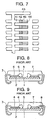
- FIG. 8 is a sectional view of a conventional resin mold type semiconductor device.
- the resin mold type semiconductor device is provided with a semiconductor chip 1, an insulating tape 2, a lead 3, a metal plating, a ball 5, a wire 6 and molded resin 7.
- the resin mold type semiconductor device has a LOC (Lead On Chip) structure which the lead 3 is adhered to a surface of the semiconductor chip 1 by the insulating tape 2.
- LOC Lead On Chip
- a space between a side of a package and the semiconductor chip 1 tends to be narrow as the semiconductor chip (pellet) 1 becomes larger. This is caused by that the package can not made larger, because the size of the package, which stores the semiconductor chip 1, is standardized though the semiconductor chip 1 is made larger.
- the insulating tape 2 tends to absorb water, therefore, there are many cases that the crack 8 is caused by the insulating tape 2.
- the insulating tape 2 also prevents the semiconductor device from making thinner.
- a semiconductor device comprises a semiconductor chip; a lead member arranged in a manner that an one side face of a head portion thereof touches a surface of the semiconductor chip; a wire for electrically connecting the surface of the semiconductor chip and another side face of the lead member; an adhesive member for adhering the one side face of the lead member and a peripheral face of the semiconductor chip; and, a package for molding the semiconductor chip, a part of the lead member, the wire and the adhesive member by synthetic resin.
- the one side face of the lead member and the peripheral face of the semiconductor chip are adhered by the adhesive member, therefore, there is no case that the thickness of the semiconductor chip increases by the adhesive member and the semiconductor device can be made thinner.
- the adhesive member is arranged so as to adhere the peripheral face of the semiconductor chip and the one side face of the lead member, therefore, the area taken by the adhesive is small. As the result, the adsorption of water can be reduced and a resin crack hardly occurs during substrate mounting.
- a semiconductor device comprises a semiconductor chip; a lead arranged in a manner that an one side face of a head portion thereof touches a surface of the semiconductor chip and provided with a concave portion in the one side face; a wire for electrically connecting the surface of the semiconductor chip and another side face of the lead member; an adhesive member for adhering the one side face of the lead member and a corner portion including a part of the surface and a part of the peripheral face of the semiconductor chip; and, a package for molding the semiconductor chip, a part of the lead member, the wire and the adhesive member by synthetic resin.
- the concave portion is provided in the lead member, therefore, the adhesive member is also applied to the concave portion and the lead member is adhered to the corner portion of the semiconductor chip.
- the adherent area becomes larger and the adherent strength can be kept. Further, the adhesive member is not forced out.
- the lead member is provided a groove extending from the concave portion to an end of the lead member.
- the adhesive member is applied to both of the concave portion and the groove.
- the corner portion of the semiconductor chip are adhered to the one side face of the lead member.
- the adherent area becomes larger, so that the adherent strength can be kept. Further, the adhesive member is not forced out.
- an assembling method of a semiconductor device comprises (a) a step of determining a amount of adhesive to be applied to a lead member; (b) a step of applying the amount of the adhesive to an one side face of a lead member; (c) a step of adhering the one side face of the lead member and a peripheral face of a semiconductor chip by the adhesive; (d) a step of fixing the lead member and the semiconductor chip by drying the adhesive; (e) a step of electrically connecting the semiconductor chip and the lead member through a wire; and, (f) a step of forming a package by molding the semiconductor chip, the lead member and the wire with synthetic resin.
- the determined amount of the adhesive is applied to the one side face of the lead member, and then the one side face of the lead member is adhered to the peripheral face of the semiconductor chip.
- FIG. 1 is a sectional view illustrating a resin mold type semiconductor device according to the first embodiment of the present invention.
- a resin mold type semiconductor device 10 is provided with a semiconductor chip 11, leads 12, wires 13, a molding resin 14 and adhesive (liquid synthetic resin) 15.
- the semiconductor chip 11 is electrically connected with the leads 12 though wires 13.
- the lead 12 is attached to the semiconductor chip 11 in a manner that a adhesion side 12b of a head portion 12a thereof touches a surface 11a of the semiconductor chip 11.
- the adhesive 15 is previously applied to the adhesion side 12b of the lead 12 at a position corresponding to the peripheral face 11b of the semiconductor chip 11, and the semiconductor chip 11 is adhered thereto.
- the semiconductor chip 11, the leads 12, the wires 13 and the liquid adhesive resin 15 are molded by the synthetic resin 14 in a manner that parts of the leads 12 project to the outside, whereby a package is assembled.
- the leads 12 and semiconductor chip 11 are adhered and fixed by the adhesive 15 at the peripheral face 11b of the semiconductor chip 11, therefore, there is no case that the thickness of the semiconductor device increases by adhesive, so that the semiconductor device can be made thinner.
- the adhesive 15 is applied only to each lead 12, that is, the area which the adhesive 15 is applied is small. Thus, absorption of water can be reduced, so that a crack occurs hardly during substrate mounting.
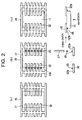
- a lead frame 16 is provided with plural leads 12 touching the surface 11a of the semiconductor chip 11.
- a predetermined amount of the adhesive 15 is applied to the lead 12 with a dispenser 17 by using pressure.
- the adhesive 15 is applied to the adhesion side 12b of each lead 12 at the position corresponding to the peripheral face 11b of the semiconductor chip 11.
- the position, to which the adhesive 15 is applied may be any position at which the peripheral face 11b of the semiconductor chip 11 is adhered to the adhesion side 12b of the lead 12.
- the lead frame 16 is turned over, and then the semiconductor chip 11 is adhered to the lead 12.
- the adhesive 15 is dried to fix the semiconductor chip 11 and the lead 12. Thereafter, usual process are performed.
- the predetermined amount of the liquid adhesive resin 15 is applied to the adhesion side 12b of the lead 12 at the position corresponding to the peripheral face 11b of the semiconductor chip 11, and the adhesion side 12b of the head portion 12a of the lead 12 touches the surface 11a of the semiconductor chip 11.
- the lead frame 16 is provided with plural leads 12 touching the surface 11a of the semiconductor chip 11.
- the leads 12 of the lead frame 16, as shown in FIG. 3(a), are passed though an adhesive dipping tank (adhesive applying unit) 21a including adhesive (liquid synthetic resin) 22 in an assembling machine of a semiconductor device so as to apply the adhesive 22 only to needed positions, namely, positions at which the adhesive 22 is touched to the leads 12.
- adhesive dipping tank 21a application positions of the adhesive 22 can be varied in accordance with the size of the semiconductor chip 11. Then, the predetermined amount of the adhesive 22 is applied to each lead 12 (see FIG. 3(b)).
- the lead 12, which the adhesive 22 is applied is conveyed to a lead frame keeping tank (keeping unit) 21b.
- the semiconductor chip 11 is fitted and adhered to the adhesion side 12b of the lead 12 by the adhesive 22 in an adhering unit (not shown).
- the adhesive 22 is dried, and the semiconductor chip 11 and the lead 12 are fixed in a drying-fixing unit (not shown).
- the semiconductor chip 11 is electrically connected with the leads 12 through the wires 13 in a connecting unit (not shown), and the semiconductor chip 11, leads 12, wires 13 and the like are resin-molded in a package forming unit (not shown). Thereafter, usual processes are performed.
- the lead frame 16 is passed though the adhesive dipping tank 21a so as to apply the adhesive 22 to the lead 12, that is, the adhesive 22 is applied to the lead in the state that the adhesion side 12b of the lead 12 faces downward.
- the adhesive 22 is applied to the lead in the state that the adhesion side 12b of the lead 12 faces downward.
- the adhesive 22 may be any adhesive member which adheres the semiconductor chip 11 and the lead 12.
- FIG. 4 is a sectional view illustrating a resin mold type semiconductor device according to the second embodiment.
- FIG. 5 is a partial plan view illustrating a lead frame of the resin mold type semiconductor device.
- a lead 31 of a resin mold type semiconductor device 30 is provided with a concave portion 32 in a adhesion side (one side face) 31b thereof.
- the concave portion 32 is formed into half-etching, that is, the lead 31 is etched to the half of the thickness thereof by solution or the like.
- the concave portion 32 may be formed into any form and by any method.
- the semiconductor chip 11 and the lead 31 of the lead frame 33 are arranged in a manner that a head portion of the lead 31 touches the surface 11a of the semiconductor chip 11, and are electrically connected through the wire 13, similarly to the resin mold type semiconductor device 10.
- the vicinity of a corner 11c of the semiconductor chip 11 is fixed to a adhesion side 31b of the lead 31 by adhesive 35. That is, the vicinity of the corner 11c includes a part of the surface 11a and a part of the peripheral face 11b of the semiconductor chip 11.
- the adhesive 35 is previously applied to the adhesion side 31b of the lead 31 at a position corresponding to the peripheral face 11b of the semiconductor chip 11. At this time, a part of the applied adhesive 35 enters the concave portion 32, and then the vicinity of the corner 11c of the semiconductor chip 11 is adhered to the adhesion side 31b of the lead 31 by the adhesive 35.
- the semiconductor chip 11, the leads 12, the wires 13 and the adhesive 15 are molded by the synthetic resin 14 in a manner that parts of the leads 12 project to the outside, whereby a package is assembled.
- the vicinity of the corner 11c of the semiconductor chip 11 is adhered to the adhesion side 31b of the lead 31 by the adhesive 35, therefore, the adherent area becomes larger, so that the adherent strength can be kept.
- the concave portion 32 is formed in the lead 31, therefore, though the adhesive 35 is applied more than the predetermined amount, an excess of the adhesive 35 enters the concave portion 32 so as not to be forced out.
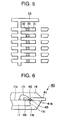
- FIG. 6 is a sectional view illustrating a resin mold type semiconductor device according to the third embodiment.
- FIG. 7 is a partial plan view illustrating a lead frame of the resin mold type semiconductor device.
- a lead 41 of a resin mold type semiconductor device 40 is provided with a concave portion 42 and a groove 46 extending from the concave portion 42 to the end portion of each lead 41 in a adhesion side (one side face) 41b thereof.
- the concave portion 42 and the groove 46 are formed into half-etching, that is, the lead 41 is etched to the half of the thickness thereof by solution or the like.
- the concave portion 42 and the groove 46 may be formed into any form and by any method.
- the semiconductor chip 11 and the lead 41 of the lead frame 43 are arranged in a manner that a head portion of the lead 41 touches the surface 11a of the semiconductor chip 11, and are electrically connected through the wire 13, similarly to the resin mold type semiconductor devices 10, 30.
- the vicinity of a corner 11c of the semiconductor chip 11 is fixed to a adhesion side 41b of the lead 41 by adhesive 45.
- the vicinity of a corner 11c includes a part of surface 11a and a part of peripheral face 11b of the semiconductor chip 11.
- the adhesive 45 is previously applied to the adhesion side 41b of the lead 41 at a position corresponding to the peripheral face 11b of the semiconductor chip 11. At this time, a part of the applied adhesive 45 enters the concave portion 42 and the groove 46, and then the vicinity of the corner 11c of the semiconductor chip 11 is adhered to the adhesion side 41b of the lead 41 by the adhesive 45.
- the semiconductor chip 11, the leads 12, the wires 13 and the adhesive 15 are molded by the synthetic resin 14 in a manner that parts of the leads 12 project to the outside, whereby a package is assembled.
- the vicinity of the corner 11c of the semiconductor chip 11 is adhered to the adhesion side 41b of the lead 41 by the adhesive 45, therefore, the adherent area becomes larger, so that the adherent strength can be kept.
- the concave portion 42 and the groove 46 are formed in the lead 41, therefore, though the adhesive 45 is applied more than the predetermined amount, an excess of the adhesive 45 enters the concave portion 42 and the groove 46 so as not to be forced out.
- Leads and a semiconductor chip are fixed by adhesive at peripheral faces of the semiconductor chip, therefore, there is no case that a thickness of a semiconductor device increases by adhesive, so that a semiconductor device can be made thinner.
- a predetermined amount of adhesive is applied to a surface of a lead at a position corresponding to a peripheral face of a semiconductor chip by pressure, and the semiconductor chip is adhered thereto, therefore, a resin mold type semiconductor device which is thin and has hardly a resin crack can be obtained.
- Adhesive is applied to a lead by passing a lead frame through a adhesive dipping tank in a state that the adhesion side of the lead faces downward, therefore, it is not necessary to turn over the lead frame, so that a semiconductor chip can be adhered to the lead frame smoothly.
- the leads and the semiconductor chip are fixed by the adhesive in the vicinity of the corner of the semiconductor chip, therefore, the adherent area becomes larger and the strength can be kept.
Landscapes
- Structures Or Materials For Encapsulating Or Coating Semiconductor Devices Or Solid State Devices (AREA)
- Encapsulation Of And Coatings For Semiconductor Or Solid State Devices (AREA)
- Lead Frames For Integrated Circuits (AREA)
- Die Bonding (AREA)
Applications Claiming Priority (2)
| Application Number | Priority Date | Filing Date | Title |
|---|---|---|---|
| JP86968/96 | 1996-04-10 | ||
| JP8086968A JPH09283545A (ja) | 1996-04-10 | 1996-04-10 | 樹脂封止型半導体装置及びその製造方法 |
Publications (3)
| Publication Number | Publication Date |
|---|---|
| EP0801424A2 true EP0801424A2 (de) | 1997-10-15 |
| EP0801424A3 EP0801424A3 (de) | 1997-10-22 |
| EP0801424B1 EP0801424B1 (de) | 2006-01-04 |
Family
ID=13901682
Family Applications (1)
| Application Number | Title | Priority Date | Filing Date |
|---|---|---|---|
| EP97105675A Expired - Lifetime EP0801424B1 (de) | 1996-04-10 | 1997-04-07 | Halbleiteranordnung und Verfahren zum Zusammensetzen derselben |
Country Status (7)
| Country | Link |
|---|---|
| US (1) | US6097083A (de) |
| EP (1) | EP0801424B1 (de) |
| JP (1) | JPH09283545A (de) |
| KR (1) | KR100366110B1 (de) |
| CN (1) | CN1091950C (de) |
| DE (1) | DE69735032T2 (de) |
| TW (1) | TW494507B (de) |
Cited By (1)
| Publication number | Priority date | Publication date | Assignee | Title |
|---|---|---|---|---|
| SG94812A1 (en) * | 2000-05-09 | 2003-03-18 | Dainippon Printing Co Ltd | Frame for semiconductor package |
Families Citing this family (2)
| Publication number | Priority date | Publication date | Assignee | Title |
|---|---|---|---|---|
| US5969410A (en) * | 1996-05-09 | 1999-10-19 | Oki Electric Industry Co., Ltd. | Semiconductor IC device having chip support element and electrodes on the same surface |
| JP2005277415A (ja) * | 2004-03-23 | 2005-10-06 | Samsung Electronics Co Ltd | リードチップ直接付着型半導体パッケージ、その製造方法及び装置 |
Family Cites Families (11)
| Publication number | Priority date | Publication date | Assignee | Title |
|---|---|---|---|---|
| JPH06105721B2 (ja) * | 1985-03-25 | 1994-12-21 | 日立超エル・エス・アイエンジニアリング株式会社 | 半導体装置 |
| US4974057A (en) * | 1986-10-31 | 1990-11-27 | Texas Instruments Incorporated | Semiconductor device package with circuit board and resin |
| JPS6437132U (de) * | 1987-08-31 | 1989-03-06 | ||
| JPH02125454A (ja) * | 1988-11-02 | 1990-05-14 | Nec Corp | 樹脂封止型半導体装置 |
| US5403785A (en) * | 1991-03-03 | 1995-04-04 | Matsushita Electric Works, Ltd. | Process of fabrication IC chip package from an IC chip carrier substrate and a leadframe and the IC chip package fabricated thereby |
| SG44840A1 (en) * | 1992-09-09 | 1997-12-19 | Texas Instruments Inc | Reduced capacitance lead frame for lead on chip package |
| JP3137518B2 (ja) * | 1993-10-29 | 2001-02-26 | 株式会社巴川製紙所 | 電子部品用液状接着剤およびそれを用いる絶縁接着層の形成方法 |
| TW270213B (de) * | 1993-12-08 | 1996-02-11 | Matsushita Electric Industrial Co Ltd | |
| US5545921A (en) * | 1994-11-04 | 1996-08-13 | International Business Machines, Corporation | Personalized area leadframe coining or half etching for reduced mechanical stress at device edge |
| JP3127195B2 (ja) * | 1994-12-06 | 2001-01-22 | シャープ株式会社 | 発光デバイスおよびその製造方法 |
| TW314650B (de) * | 1995-06-21 | 1997-09-01 | Oki Electric Ind Co Ltd |
-
1996
- 1996-04-10 JP JP8086968A patent/JPH09283545A/ja not_active Withdrawn
-
1997
- 1997-04-02 TW TW086104250A patent/TW494507B/zh not_active IP Right Cessation
- 1997-04-07 EP EP97105675A patent/EP0801424B1/de not_active Expired - Lifetime
- 1997-04-07 DE DE69735032T patent/DE69735032T2/de not_active Expired - Fee Related
- 1997-04-10 US US08/827,693 patent/US6097083A/en not_active Expired - Fee Related
- 1997-04-10 KR KR1019970013295A patent/KR100366110B1/ko not_active Expired - Fee Related
- 1997-04-10 CN CN97111651A patent/CN1091950C/zh not_active Expired - Fee Related
Cited By (1)
| Publication number | Priority date | Publication date | Assignee | Title |
|---|---|---|---|---|
| SG94812A1 (en) * | 2000-05-09 | 2003-03-18 | Dainippon Printing Co Ltd | Frame for semiconductor package |
Also Published As
| Publication number | Publication date |
|---|---|
| TW494507B (en) | 2002-07-11 |
| EP0801424A3 (de) | 1997-10-22 |
| US6097083A (en) | 2000-08-01 |
| KR970072220A (ko) | 1997-11-07 |
| KR100366110B1 (ko) | 2003-02-19 |
| EP0801424B1 (de) | 2006-01-04 |
| CN1165400A (zh) | 1997-11-19 |
| JPH09283545A (ja) | 1997-10-31 |
| DE69735032T2 (de) | 2006-08-31 |
| DE69735032D1 (de) | 2006-03-30 |
| CN1091950C (zh) | 2002-10-02 |
Similar Documents
| Publication | Publication Date | Title |
|---|---|---|
| KR100350759B1 (ko) | 볼 그리드 어레이형 반도체 장치 및 그 제조 방법 | |
| KR970006533B1 (ko) | 반도체장치 및 그 제조방법 | |
| US6258630B1 (en) | Resin-sealed semiconductor device having island for mounting semiconductor element coupled to heat spreader | |
| KR100428271B1 (ko) | 집적회로패키지와그제조방법 | |
| US6876090B2 (en) | Semiconductor chip and method for producing housing | |
| US6097083A (en) | Semiconductor device which is crack resistant | |
| US6147398A (en) | Semiconductor device package | |
| JPH0815165B2 (ja) | 樹脂絶縁型半導体装置の製造方法 | |
| KR970077548A (ko) | 유체 상태의 접착제를 이용한 반도체 칩 실장 방법 및 그에 이용되는 loc형 반도체 칩 패키지의 리드 프레임 | |
| US6040620A (en) | Lead frame for LOC having a regulating lead to prevent variation in adhesive coverage | |
| US6183589B1 (en) | Method for manufacturing lead-on-chip (LOC) semiconductor packages using liquid adhesive applied under the leads | |
| JPS62296541A (ja) | 樹脂封止型半導体装置 | |
| US5969410A (en) | Semiconductor IC device having chip support element and electrodes on the same surface | |
| KR100432348B1 (ko) | 리드온칩(loc)용리드프레임 | |
| JPH0366152A (ja) | 半導体集積回路モジュール | |
| KR19980044545A (ko) | 내부 리드를 지지하기 위한 보강재를 갖는 탭 테이프 | |
| KR940008332B1 (ko) | 효율적인 서포트링구조를 가지는 반도체 패키지장치 | |
| KR200295664Y1 (ko) | 적층형반도체패키지 | |
| JPH0366150A (ja) | 半導体集積回路装置 | |
| KR200159003Y1 (ko) | 열방출용 반도체 패키지 | |
| KR100244509B1 (ko) | 반도체 패키지의 제조방법 | |
| KR20000050381A (ko) | 리드 온 칩 패키지 | |
| KR19980077227A (ko) | 슬럿이 형성된 다이 패드와 반도체 칩의 본딩 방법 | |
| KR19990022929U (ko) | 브이·씨·에이 패키지 | |
| JPH1032286A (ja) | 半導体装置 |
Legal Events
| Date | Code | Title | Description |
|---|---|---|---|
| PUAI | Public reference made under article 153(3) epc to a published international application that has entered the european phase |
Free format text: ORIGINAL CODE: 0009012 |
|
| PUAL | Search report despatched |
Free format text: ORIGINAL CODE: 0009013 |
|
| AK | Designated contracting states |
Kind code of ref document: A2 Designated state(s): DE FR GB NL |
|
| AK | Designated contracting states |
Kind code of ref document: A3 Designated state(s): DE FR GB NL |
|
| 17P | Request for examination filed |
Effective date: 19980407 |
|
| 17Q | First examination report despatched |
Effective date: 20000830 |
|
| GRAP | Despatch of communication of intention to grant a patent |
Free format text: ORIGINAL CODE: EPIDOSNIGR1 |
|
| GRAS | Grant fee paid |
Free format text: ORIGINAL CODE: EPIDOSNIGR3 |
|
| GRAA | (expected) grant |
Free format text: ORIGINAL CODE: 0009210 |
|
| AK | Designated contracting states |
Kind code of ref document: B1 Designated state(s): DE FR GB NL |
|
| REG | Reference to a national code |
Ref country code: GB Ref legal event code: FG4D |
|
| REF | Corresponds to: |
Ref document number: 69735032 Country of ref document: DE Date of ref document: 20060330 Kind code of ref document: P |
|
| ET | Fr: translation filed | ||
| PLBE | No opposition filed within time limit |
Free format text: ORIGINAL CODE: 0009261 |
|
| STAA | Information on the status of an ep patent application or granted ep patent |
Free format text: STATUS: NO OPPOSITION FILED WITHIN TIME LIMIT |
|
| 26N | No opposition filed |
Effective date: 20061005 |
|
| PGFP | Annual fee paid to national office [announced via postgrant information from national office to epo] |
Ref country code: DE Payment date: 20070405 Year of fee payment: 11 |
|
| PGFP | Annual fee paid to national office [announced via postgrant information from national office to epo] |
Ref country code: NL Payment date: 20070415 Year of fee payment: 11 |
|
| PGFP | Annual fee paid to national office [announced via postgrant information from national office to epo] |
Ref country code: GB Payment date: 20070404 Year of fee payment: 11 |
|
| PGFP | Annual fee paid to national office [announced via postgrant information from national office to epo] |
Ref country code: FR Payment date: 20070411 Year of fee payment: 11 |
|
| GBPC | Gb: european patent ceased through non-payment of renewal fee |
Effective date: 20080407 |
|
| NLV4 | Nl: lapsed or anulled due to non-payment of the annual fee |
Effective date: 20081101 |
|
| PG25 | Lapsed in a contracting state [announced via postgrant information from national office to epo] |
Ref country code: NL Free format text: LAPSE BECAUSE OF NON-PAYMENT OF DUE FEES Effective date: 20081101 Ref country code: DE Free format text: LAPSE BECAUSE OF NON-PAYMENT OF DUE FEES Effective date: 20081101 |
|
| REG | Reference to a national code |
Ref country code: FR Ref legal event code: ST Effective date: 20081231 |
|
| PG25 | Lapsed in a contracting state [announced via postgrant information from national office to epo] |
Ref country code: FR Free format text: LAPSE BECAUSE OF NON-PAYMENT OF DUE FEES Effective date: 20080430 |
|
| PG25 | Lapsed in a contracting state [announced via postgrant information from national office to epo] |
Ref country code: GB Free format text: LAPSE BECAUSE OF NON-PAYMENT OF DUE FEES Effective date: 20080407 |