EP0801426A2 - Anordnung mit Graben-MOS-Gate und Verfahren zur Herstellung - Google Patents
Anordnung mit Graben-MOS-Gate und Verfahren zur Herstellung Download PDFInfo
- Publication number
- EP0801426A2 EP0801426A2 EP97400624A EP97400624A EP0801426A2 EP 0801426 A2 EP0801426 A2 EP 0801426A2 EP 97400624 A EP97400624 A EP 97400624A EP 97400624 A EP97400624 A EP 97400624A EP 0801426 A2 EP0801426 A2 EP 0801426A2
- Authority
- EP
- European Patent Office
- Prior art keywords
- trench
- floor
- layer
- silicon dioxide
- thickness
- Prior art date
- Legal status (The legal status is an assumption and is not a legal conclusion. Google has not performed a legal analysis and makes no representation as to the accuracy of the status listed.)
- Granted
Links
Images


Classifications
-
- H—ELECTRICITY
- H10—SEMICONDUCTOR DEVICES; ELECTRIC SOLID-STATE DEVICES NOT OTHERWISE PROVIDED FOR
- H10D—INORGANIC ELECTRIC SEMICONDUCTOR DEVICES
- H10D30/00—Field-effect transistors [FET]
- H10D30/60—Insulated-gate field-effect transistors [IGFET]
- H10D30/64—Double-diffused metal-oxide semiconductor [DMOS] FETs
- H10D30/66—Vertical DMOS [VDMOS] FETs
- H10D30/668—Vertical DMOS [VDMOS] FETs having trench gate electrodes, e.g. UMOS transistors
-
- H—ELECTRICITY
- H10—SEMICONDUCTOR DEVICES; ELECTRIC SOLID-STATE DEVICES NOT OTHERWISE PROVIDED FOR
- H10D—INORGANIC ELECTRIC SEMICONDUCTOR DEVICES
- H10D30/00—Field-effect transistors [FET]
- H10D30/01—Manufacture or treatment
- H10D30/021—Manufacture or treatment of FETs having insulated gates [IGFET]
- H10D30/028—Manufacture or treatment of FETs having insulated gates [IGFET] of double-diffused metal oxide semiconductor [DMOS] FETs
- H10D30/0291—Manufacture or treatment of FETs having insulated gates [IGFET] of double-diffused metal oxide semiconductor [DMOS] FETs of vertical DMOS [VDMOS] FETs
- H10D30/0297—Manufacture or treatment of FETs having insulated gates [IGFET] of double-diffused metal oxide semiconductor [DMOS] FETs of vertical DMOS [VDMOS] FETs using recessing of the gate electrodes, e.g. to form trench gate electrodes
-
- H—ELECTRICITY
- H10—SEMICONDUCTOR DEVICES; ELECTRIC SOLID-STATE DEVICES NOT OTHERWISE PROVIDED FOR
- H10D—INORGANIC ELECTRIC SEMICONDUCTOR DEVICES
- H10D64/00—Electrodes of devices having potential barriers
- H10D64/01—Manufacture or treatment
- H10D64/013—Manufacture or treatment of electrodes having a conductor capacitively coupled to a semiconductor by an insulator
- H10D64/01302—Manufacture or treatment of electrodes having a conductor capacitively coupled to a semiconductor by an insulator the insulator being formed after the semiconductor body, the semiconductor being silicon
- H10D64/01332—Making the insulator
- H10D64/01336—Making the insulator on single crystalline silicon, e.g. chemical oxidation using a liquid
- H10D64/0134—Making the insulator on single crystalline silicon, e.g. chemical oxidation using a liquid with a treatment, e.g. annealing, after the formation of the insulator and before the formation of the conductor
-
- H—ELECTRICITY
- H10—SEMICONDUCTOR DEVICES; ELECTRIC SOLID-STATE DEVICES NOT OTHERWISE PROVIDED FOR
- H10D—INORGANIC ELECTRIC SEMICONDUCTOR DEVICES
- H10D64/00—Electrodes of devices having potential barriers
- H10D64/01—Manufacture or treatment
- H10D64/013—Manufacture or treatment of electrodes having a conductor capacitively coupled to a semiconductor by an insulator
- H10D64/01302—Manufacture or treatment of electrodes having a conductor capacitively coupled to a semiconductor by an insulator the insulator being formed after the semiconductor body, the semiconductor being silicon
- H10D64/01332—Making the insulator
- H10D64/01336—Making the insulator on single crystalline silicon, e.g. chemical oxidation using a liquid
- H10D64/01342—Making the insulator on single crystalline silicon, e.g. chemical oxidation using a liquid by deposition, e.g. evaporation, ALD or laser deposition
-
- H—ELECTRICITY
- H10—SEMICONDUCTOR DEVICES; ELECTRIC SOLID-STATE DEVICES NOT OTHERWISE PROVIDED FOR
- H10D—INORGANIC ELECTRIC SEMICONDUCTOR DEVICES
- H10D64/00—Electrodes of devices having potential barriers
- H10D64/01—Manufacture or treatment
- H10D64/013—Manufacture or treatment of electrodes having a conductor capacitively coupled to a semiconductor by an insulator
- H10D64/01302—Manufacture or treatment of electrodes having a conductor capacitively coupled to a semiconductor by an insulator the insulator being formed after the semiconductor body, the semiconductor being silicon
- H10D64/01332—Making the insulator
- H10D64/01336—Making the insulator on single crystalline silicon, e.g. chemical oxidation using a liquid
- H10D64/01344—Making the insulator on single crystalline silicon, e.g. chemical oxidation using a liquid in a nitrogen-containing ambient, e.g. N2O oxidation
-
- H—ELECTRICITY
- H10—SEMICONDUCTOR DEVICES; ELECTRIC SOLID-STATE DEVICES NOT OTHERWISE PROVIDED FOR
- H10D—INORGANIC ELECTRIC SEMICONDUCTOR DEVICES
- H10D64/00—Electrodes of devices having potential barriers
- H10D64/01—Manufacture or treatment
- H10D64/013—Manufacture or treatment of electrodes having a conductor capacitively coupled to a semiconductor by an insulator
- H10D64/01302—Manufacture or treatment of electrodes having a conductor capacitively coupled to a semiconductor by an insulator the insulator being formed after the semiconductor body, the semiconductor being silicon
- H10D64/01332—Making the insulator
- H10D64/01336—Making the insulator on single crystalline silicon, e.g. chemical oxidation using a liquid
- H10D64/01346—Making the insulator on single crystalline silicon, e.g. chemical oxidation using a liquid in a gaseous ambient using an oxygen or a water vapour, e.g. oxidation through a layer
-
- H—ELECTRICITY
- H10—SEMICONDUCTOR DEVICES; ELECTRIC SOLID-STATE DEVICES NOT OTHERWISE PROVIDED FOR
- H10D—INORGANIC ELECTRIC SEMICONDUCTOR DEVICES
- H10D64/00—Electrodes of devices having potential barriers
- H10D64/60—Electrodes characterised by their materials
- H10D64/66—Electrodes having a conductor capacitively coupled to a semiconductor by an insulator, e.g. MIS electrodes
- H10D64/68—Electrodes having a conductor capacitively coupled to a semiconductor by an insulator, e.g. MIS electrodes characterised by the insulator, e.g. by the gate insulator
- H10D64/681—Electrodes having a conductor capacitively coupled to a semiconductor by an insulator, e.g. MIS electrodes characterised by the insulator, e.g. by the gate insulator having a compositional variation, e.g. multilayered
- H10D64/685—Electrodes having a conductor capacitively coupled to a semiconductor by an insulator, e.g. MIS electrodes characterised by the insulator, e.g. by the gate insulator having a compositional variation, e.g. multilayered being perpendicular to the channel plane
-
- H—ELECTRICITY
- H10—SEMICONDUCTOR DEVICES; ELECTRIC SOLID-STATE DEVICES NOT OTHERWISE PROVIDED FOR
- H10D—INORGANIC ELECTRIC SEMICONDUCTOR DEVICES
- H10D64/00—Electrodes of devices having potential barriers
- H10D64/60—Electrodes characterised by their materials
- H10D64/66—Electrodes having a conductor capacitively coupled to a semiconductor by an insulator, e.g. MIS electrodes
- H10D64/68—Electrodes having a conductor capacitively coupled to a semiconductor by an insulator, e.g. MIS electrodes characterised by the insulator, e.g. by the gate insulator
- H10D64/693—Electrodes having a conductor capacitively coupled to a semiconductor by an insulator, e.g. MIS electrodes characterised by the insulator, e.g. by the gate insulator the insulator comprising nitrogen, e.g. nitrides, oxynitrides or nitrogen-doped materials
-
- H—ELECTRICITY
- H10—SEMICONDUCTOR DEVICES; ELECTRIC SOLID-STATE DEVICES NOT OTHERWISE PROVIDED FOR
- H10D—INORGANIC ELECTRIC SEMICONDUCTOR DEVICES
- H10D64/00—Electrodes of devices having potential barriers
- H10D64/20—Electrodes characterised by their shapes, relative sizes or dispositions
- H10D64/27—Electrodes not carrying the current to be rectified, amplified, oscillated or switched, e.g. gates
- H10D64/311—Gate electrodes for field-effect devices
- H10D64/411—Gate electrodes for field-effect devices for FETs
- H10D64/511—Gate electrodes for field-effect devices for FETs for IGFETs
- H10D64/514—Gate electrodes for field-effect devices for FETs for IGFETs characterised by the insulating layers
- H10D64/516—Gate electrodes for field-effect devices for FETs for IGFETs characterised by the insulating layers the thicknesses being non-uniform
-
- H—ELECTRICITY
- H10—SEMICONDUCTOR DEVICES; ELECTRIC SOLID-STATE DEVICES NOT OTHERWISE PROVIDED FOR
- H10D—INORGANIC ELECTRIC SEMICONDUCTOR DEVICES
- H10D64/00—Electrodes of devices having potential barriers
- H10D64/60—Electrodes characterised by their materials
- H10D64/66—Electrodes having a conductor capacitively coupled to a semiconductor by an insulator, e.g. MIS electrodes
- H10D64/68—Electrodes having a conductor capacitively coupled to a semiconductor by an insulator, e.g. MIS electrodes characterised by the insulator, e.g. by the gate insulator
- H10D64/681—Electrodes having a conductor capacitively coupled to a semiconductor by an insulator, e.g. MIS electrodes characterised by the insulator, e.g. by the gate insulator having a compositional variation, e.g. multilayered
Definitions
- the present invention relates to MOS devices and, more particularly, to a trench MOS gate device and a process for forming same.
- An MOS transistor that includes a trench gate structure offers important advantages over a planar transistor for high current, low voltage switching applications. In the latter configuration, constriction occurs at high current flows, an effect that places substantial constraints on the design of a transistor intended for operation under such conditions.
- a trench gate of a DMOS device typically includes a trench extending from the source to the drain and having sidewalls and a floor that are each lined with a layer of thermally grown silicon dioxide.
- the lined trench is filled with doped polysilicon.
- the structure of the trench gate allows less constricted current flow and, consequently, provides lower values of specific on-resistance.
- the trench gate makes possible a decreased cell pitch in an MOS channel extending along the vertical sidewalls of the trench from the bottom of the source across the body of the transistor to the drain below. Channel density is thereby increased, which reduces the contribution of the channel to on-resistance.
- trench DMOS transistors The structure and performance of trench DMOS transistors are discussed in Bulucea and Rossen, "Trench DMOS Transistor Technology for High-Current (100 A Range) Switching" in Solid-State Electronics , 1991, Vol. 34, No. 5, pg. 493-507.
- trench gates are also advantageously employed in insulated gate bipolar transistors (IGBTs), MOS-controlled thyristors (MCTs), and other MOS gated device structures.
- Trenches lined with oxide dielectric and filled with polysilicon as a means of providing lateral isolation for component islands situated within the trench regions are disclosed in specifications of U.S. Patent Nos. 5,196,373 and 5,248,894.
- a preferred method of forming the dielectric for this purpose is conventional thermal oxidation.
- Thermal oxidation to produce silicon dioxide for isolation of component islands does not require the control of oxide layer thickness provided by the device and process of the present invention.
- the dielectric used for isolation is very thick, often thicker than 10,000 angstroms. In this thickness range, the oxide grows according to a parabolic growth rule that produces the same growth rate on all crystal surfaces rather than by the orientation dependent linear growth rate that applies to the hundreds of angstroms thickness range relevant for gate oxides. Consequently, thermally grown oxides for isolation purposes have essentially the same thickness on all surfaces.
- a thin, approximately 100-angstrom thick thermal oxide layer is sometimes grown to cover an island surface. This thin oxide layer is then covered with a thick deposited oxide layer of about 10,000 angstroms to provide the required isolation. In such instances, the isolation layer consists almost entirely of deposited oxide. This layer must be thick enough to ensure that average capacitance is low and that the oxide rupture voltage is higher than the maximum voltage to be isolated. However, there are no minimum thickness or uniformity constraints for oxide layers intended for isolation of component islands.
- the trench gate structure is beneficial for the operation of a transistor at higher currents, its performance can be degraded by the formation of a gate-to-drain capacitance across the dielectric material in the bottom of the trench. Furthermore, the bottom corners of the trench can cause concentration of an electric field when the DMOS is reverse biased, resulting in reduced breakdown voltage. These effects can be mitigated by beneficially controlling the formation of the dielectric layers on the sidewalls and floor of the gate trench, which is provided by the present invention.
- the present invention includes a trench MOS gate comprising, a trench having a floor and sidewalls, said floor and said sidewalls comprising a layer of a dielectric material, said floor layer and said sidewall layers each having a substantially uniform controlled thickness dimension, characterized in that said substantially uniform thickness dimensions are related by a controlled floor to sidewall layer thickness ratio, said ratio being established by individually controlling the substantially uniform thickness of each of said floor and sidewall layers.
- the invention also includes a process for forming an improved trench MOS gate device comprising the steps of, forming a trench in a silicon device wafer, said trench having a floor and sidewalls, forming a layer of dielectric material on each of said floor and said sidewalls, said floor layer and said sidewall layers each having a substantially uniform controlled thickness dimension, said substantially uniform thickness dimensions being related by a controlled floor to sidewall layer thickness ratio, said ratio being controlled by individually controlling the substantially uniform thickness of each of said floor and sidewall layers, filling said trench containing said layers of dielectric material with polysilicon, applying an insulator over said polysilicon, so as to form a trench gate, and forming a patterned electrically conducting metallic interconnect on said trench gate.
- a trench MOS gate device comprises a trench whose floor and sidewalls include layers of dielectric material, the layers each having a controlled thickness dimension. These thickness dimensions are related by a controlled floor:sidewall layer thickness ratio, which is established by individually controlling the thickness of each of the floor and sidewall dielectric layers. This floor to sidewall layer thickness ratio is preferably at least 1 to 1, more preferably at least 1.2 to 1.
- the process for forming a trench MOS gate device comprises etching a trench in a silicon device wafer and forming layers of dielectric material on the trench floor and on the sidewalls, each layer having a controlled thickness dimension.
- the thickness dimensions are related by a controlled floor to sidewall layer thickness ratio that is preferably at least 1 to 1.
- the layers preferably comprise a composite of thermally grown and deposited silicon dioxide.
- the trench containing the dielectric layers is filled with polysilicon, and an insulator layer is formed over the polysilicon, thereby forming a trench gate.
- a patterned electrically conducting metallic interconnect is formed over the trench gate.
- the trench MOS gate device includes a trench gate having a trench provided with layers of dielectric material of an advantageously controlled thickness ratio on the floor and the sidewalls, which reduces the damage caused by undesirable parasitic effects.
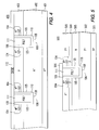
- FIG. 1 is a schematic representation of a trench gate structure of a DMOS transistor of the present invention.
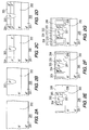
- FIG. 2 schematically depicts a process embodiment of the invention.
- FIG. 3 is a schematic representation of a further process embodiment of the invention.
- FIG. 4 schematically represents a trench gate structure of an IGBT of the invention.
- FIG. 5 schematically depicts a trench gate structure for an MCT of the invention.
- thermally grown oxide will form layers of different thicknesses on sidewalls having different crystalline orientations.
- Channel resistance will be higher for the channel segments with thicker oxide, resulting in nonuniform current distribution among the channel segments. This is another undesirable effect of the crystal orientation-dependent growth rate of the gate oxide.
- a first portion of the gate oxide is formed by thermal oxidation to achieve a low interface state density.
- the rest of the gate oxide is formed by chemical vapor deposition, which has a higher deposition rate on horizontal surfaces (such as the trench floor) than it does on vertical surfaces (such as the sidewalls). The faster deposition rate on horizontal surfaces compensates for the slower thermal oxide growth rate on those surfaces so that the composite oxide layer can be thicker on the floor than on the sidewalls.
- a system useful for depositing gate oxide in accordance with the present invention employs a Novellus Concept 1 dielectric deposition apparatus, available from Novellus Corp. Such systems can deposit oxide by plasma CVD at a deposition rate ratio of about 2 to 1 on horizontal versus vertical surfaces. A ratio of greater than 1.5 to 1 is preferred.
- a composite oxide having a sidewall total layer thickness of 500 angstroms may be formed on (110) trench sidewalls and (100) trench bottoms as follows: a 250-angstrom thermal oxide layer is grown on the trench sidewalls, along with a simultaneously grown 177-angstrom layer on the trench floor. A 250-angstrom layer of oxide is deposited on the sidewalls over the grown oxide, while a 500 angstrom-thick oxide layer is simultaneously deposited on the floor of the trench.
- the result of this composite gate oxide formation process is a 500-angstrom thick sidewall oxide layer and a 677-angstrom thick floor oxide layer. This produces the desirable result of thicker floor oxide to suppress parasitic features together with thinner sidewall oxide to minimize channel resistance, a result opposite to that obtained with a conventional dielectricforming growth process, in which the sidewall oxide is thicker than the floor oxide.
- the ratio of floor to sidewall oxide layer thicknesses can be adjusted over a wide range by adjusting the ratio of the thickness of the thermal to the deposited oxide.
- the performance of a device can be optimized to a degree not possible using the conventional thermal oxidation process.
- FIG. 1 schematically depicts a trench gate structure 100 for a DMOS transistor.
- Substrate 101 is an N + silicon wafer on which is grown an N - layer that provides a drain region 102.
- a P - body region 103 is formed by doping, and N + source regions 104 are formed in the body region 103 by masked ion implant. The difference between the body region 103 and the source region 104 diffusions defines the length of the channels 105.
- Trenches 106 formed by patterned etching extend through portions of source regions 104 and body region 103 into drain region 102.
- Trenches 106 have sidewalls 107 and a floor 108.
- Sidewalls 107 and floor 108 each include layers 109 and 110, respectively, of silicon dioxide.
- the thickness of floor layer 110 is greater than that of sidewall layers 109.
- Layers 109 and 110 comprise a composite of thermally grown and deposited silicon oxide.
- Trenches 106 further contain highly doped polysilicon 111.
- An insulator layer 112 is formed over the polysilicon 111, which forms a gate between the source regions 104 and the drain region 102.
- the DMOS transistor of the invention is obtained from the trench gate structure 100 by forming contact apertures, interconnect metal, and a patterned dielectric protection layer over the metal, all not shown in FIG.1.
- the composite oxide contained in layers 109 and 110 comprises thermally grown silicon dioxide, produced by the reaction of silicon in an oxygen atmosphere, and deposited silicon dioxide, obtained by deposition of the reaction product of a volatile silicon-containing compound.
- the thickness of the floor layer 110 which may be in the range of about 300 to 3,000 angstroms, is greater than that of the sidewall layers 109, which may be in the range of 200 to 1,500 angstroms.
- the trench 106 included in a transistor may have an open-cell stripe topology or, preferably, a closed-cell cellular topology. Furthermore, the cellular topology of the trench 106 may have a square or, more preferably, a hexagonal configuration.
- FIGS. 2A-G A process sequence useful to make a trench gate device for a DMOS transistor is illustrated in FIGS. 2A-G, which are not to scale.
- the process begins with a silicon wafer 200 having an N + layer 201 of (100) crystal orientation.
- An N - silicon layer that provides a drain region 202 is grown on layer 201 using conventional epitaxial growth methods (FIG. 2A).
- the thickness and resistivity of the layer 202 are chosen to support the desired breakdown voltage while minimizing the on-resistance.
- P + body contacts 203 are optionally formed by masked ion implant and diffusion into selected areas of the wafer surface to act as low resistance body contacts (FIG. 2B).
- the body contacts 203 may optionally be formed later in the process or omitted.
- a P - body region 204 that overlaps the P + body contacts 203 is formed (FIG. 2C).
- the doping profile of the body region 204 is chosen such that the desired threshold voltage will be obtained after the source and trench gates have been formed in the body.
- the depth of the body junction depth is about 2 microns.
- N + source regions 205 are formed in the body region 204 by masked ion implant such that they abut the body contacts 203 (FIG. 2D).
- the depth of the source region 205 is conveniently about 1 micron and is chosen to give the desired channel length.
- the channel length which is the difference between the depths of the body and source diffusions, is about 1 micron.
- the trench pattern is formed in a suitable mask, and a trench 206 is etched through the exposed portions of source regions 205 and body region 204 into the underlying drain region 202 by reactive ion etching (RIE) (FIG. 2E).
- RIE reactive ion etching
- the composite gate oxide is formed from thermally grown and deposited oxide on the exposed sidewalls and bottom of the trench, providing sidewall oxide layers 207 and bottom oxide layer 208. Preferably, this is carried out as previously described in this disclosure.
- the remainder of the trench 206 is filled with polysilicon 209, and the polysilicon 209 is planarized by, for example, chemical-mechanical planarization (FIG. 2F).
- the device fabrication is completed by forming an oxide insulator 210 over the gate polysilicon 209; forming contact apertures through the insulator to source, body contacts, and gate regions (not shown); applying a patterned electrically conducting metallic interconnect 211; and applying a dielectric protection layer 212 over the interconnect 211 (FIG. 2G).
- Drain body junction breakdown maximization structures which are not shown because they do not appear in the interior cellular part of the device, may be formed around the perimeter of the device.
- the thermally grown portion of the composite gate oxide may, for example, be grown in O 2 at 900°C to a thickness of 175 angstroms on (100) crystal surfaces.
- a chlorine containing compound such as HCI may be included in the oxidizing atmosphere to remove metallic impurities.
- the deposited portion of the composite oxide may be formed using a Novellus plasma CVD deposition system to a thickness, for example, of 500 angstroms on horizontal surfaces.
- O 2 and tetraethoxysilane (TEOS) source gases may be employed at a deposition temperature of about 400°C.
- the deposited oxide may be densified after deposition by annealing it in a diffusion furnace at 950°C in a nitrogen atmosphere that optionally contains a small oxygen concentration.
- FIGS. 3A-C Another embodiment of the process of the invention that produces a thicker layer of oxide on the bottom than on the sidewalls in a trench gate structure is illustrated in FIGS. 3A-C, which are not to scale.
- the process is the same through the trench etch step as in the previously depicted process (FIGS. 2A-E).
- the portions of the nitride layer 302 in the bottoms of the trenches and also on the wafer top surface is removed by a nonmasked anisotropic reactive ion etch (FIG. 3B), which attacks only material on horizontal surfaces. These surfaces are perpendicular to the direction of flight of the etch ions in the etch chamber.
- FOG. 3B nonmasked anisotropic reactive ion etch
- a layer 303 comprising a second portion of gate oxide is then grown to provide a total thickness of, for example, 1000 angstroms on the surfaces not covered by nitride, including the trench bottom.
- the residual vertical nitride layer 302 protects the trench sidewalls from oxidation in the well known local oxidation process.
- the residual nitride layer 302 is preferably stripped after the formation of the oxide layer 303. This leaves the trench 206 with a 700-angstrom layer of oxide provided by layer 301 on the sidewalls and a desirably thicker 1000-angstrom layer of oxide provided by layers 301 and 303 together on its bottom (FIG. 3C).
- the trench 206 is filled with doped polysilicon, and the construction of the transistor is completed as illustrated by FIGS. 2F-G.
- the trench gate oxide which is preferably a composite of thermally grown and deposited oxide, in the device and process of the present invention is sufficiently thin to provide low on-resistance and has constant thickness on all sidewalls to provide equal current flow on the sidewall surfaces. Its interface charge density is low enough to provide low and controlled threshold voltage, and its floor layer thickness is sufficient to minimize capacitance and provide required oxide and junction breakdown.
- FIG. 4 is a schematic representation of another embodiment a trench gate structure 400 for an insulated gate bipolar transistor (IGBT).
- Structure 400 includes a P + type substrate 401, an N - typed epitaxial layer 402, and body 403.
- the substrate 401 is the anode of the IGBT.
- the lightly doped layer 402 is a drift layer that supports high voltage when the device is off.
- the remaining components in structure 400 are as described for structure100 of FIG. 1.
- the thickness of oxide layers 109 and 110 on sidewalls 107 and floor 108, respectively, of trenches 106 of structure 100 are advantageously controlled, as described for structure 100.
- FIG. 5 schematically illustrates, as a further embodiment, a trench gate structure 500 in a P type MOS controlled thyristor (MCT).
- MCT P type MOS controlled thyristor
- This structure includes an N + substrate 501, on which is grown a P - epitaxial layer 502.
- Structure 500 further comprises N type drift region 503, a P type body 504, and a P + anode region 505.
- Substrate 501 provides the cathode region.
- Analogous gate structures useful for N type MCTs can also be constructed, in which case the conductivity type of all regions would be opposite to those depicted for structure 500.
- An insulator layer 506 is formed over polysilicon 111.
- the other components depicted in structure 500 are as described for structure 100 of FIG. 1.
- the oxide layers 109 and 110 of structure 500 are characterized by a beneficially controlled thickness ratio.
- a trench MOS gate device that comprises a trench whose floor and sidewalls include layers of dielectric material, having a controlled thickness dimension. These thickness dimensions are related by a controlled floor:sidewall layer thickness ratio, which is established by individually controlling the thickness of each of the floor and sidewall dielectric layers. This floor to sidewall layer thickness ratio is at least 1 to 1, and preferably at least 1.2 to 1.
- a process for forming a trench MOS gate device comprises etching a trench in a silicon device wafer and forming layers of dielectric material on the trench floor and on the sidewalls, each layer having a controlled thickness dimension, related by a controlled floor to sidewall layer thickness ratio that is preferably at least 1 to 1.
- the layers preferably comprise a composite of thermally grown and deposited silicon dioxide.
Landscapes
- Insulated Gate Type Field-Effect Transistor (AREA)
- Thyristors (AREA)
Applications Claiming Priority (2)
| Application Number | Priority Date | Filing Date | Title |
|---|---|---|---|
| US636904 | 1996-04-10 | ||
| US08/636,904 US5770878A (en) | 1996-04-10 | 1996-04-10 | Trench MOS gate device |
Publications (3)
| Publication Number | Publication Date |
|---|---|
| EP0801426A2 true EP0801426A2 (de) | 1997-10-15 |
| EP0801426A3 EP0801426A3 (de) | 1998-09-30 |
| EP0801426B1 EP0801426B1 (de) | 2008-05-14 |
Family
ID=24553828
Family Applications (1)
| Application Number | Title | Priority Date | Filing Date |
|---|---|---|---|
| EP97400624A Expired - Lifetime EP0801426B1 (de) | 1996-04-10 | 1997-03-20 | Verfahren zur Herstellung einer Anordnung mit Graben-MOS-Gate |
Country Status (4)
| Country | Link |
|---|---|
| US (2) | US5770878A (de) |
| EP (1) | EP0801426B1 (de) |
| JP (1) | JP4029946B2 (de) |
| DE (1) | DE69738681D1 (de) |
Cited By (14)
| Publication number | Priority date | Publication date | Assignee | Title |
|---|---|---|---|---|
| US6265304B1 (en) * | 1999-10-05 | 2001-07-24 | Advanced Micron Devices, Inc. | Controlling an etching process of multiple layers based upon thickness ratio of the dielectric layers |
| WO2003015180A3 (en) * | 2001-08-10 | 2003-11-06 | Siliconix Inc | Mis device having a trench gate electrode and method of making the same |
| EP1186019A4 (de) * | 1999-05-25 | 2004-05-26 | Richard K Williams | Grabenhalbleiter mit gatteroxiden verschiedener dicke und seine herstellung |
| WO2004055882A1 (en) * | 2002-12-14 | 2004-07-01 | Koninklijke Philips Electronics N.V. | Method of manufacturing a trench-gate semiconductor device |
| US6764906B2 (en) | 2001-07-03 | 2004-07-20 | Siliconix Incorporated | Method for making trench mosfet having implanted drain-drift region |
| WO2004061975A1 (en) * | 2002-12-19 | 2004-07-22 | Siliconix Incorporated | Trench mis device having implanted drain-drift region and thick bottom oxide and process for manufacturing the same |
| EP1376675A3 (de) * | 2002-06-21 | 2005-01-19 | Siliconix incorporated | Verfahren zur Herstellung eines Graben-MOSFETs |
| US6849898B2 (en) | 2001-08-10 | 2005-02-01 | Siliconix Incorporated | Trench MIS device with active trench corners and thick bottom oxide |
| US7009247B2 (en) | 2001-07-03 | 2006-03-07 | Siliconix Incorporated | Trench MIS device with thick oxide layer in bottom of gate contact trench |
| US7033876B2 (en) | 2001-07-03 | 2006-04-25 | Siliconix Incorporated | Trench MIS device having implanted drain-drift region and thick bottom oxide and process for manufacturing the same |
| EP1761953A4 (de) * | 2004-06-30 | 2009-02-25 | Advanced Analogic Tech Inc | Graben-mosfet mit ausgesparter klemmdiode |
| CN100508210C (zh) * | 2002-12-19 | 2009-07-01 | 西利康尼克斯股份有限公司 | 具有注入漏极漂移区和厚底部氧化物的沟槽金属-绝缘体-半导体器件及其制造方法 |
| US7592228B2 (en) | 1999-05-25 | 2009-09-22 | Advanced Analogic Technologies, Inc. | Recessed clamping diode fabrication in trench devices |
| EP2070108A4 (de) * | 2006-09-27 | 2010-12-01 | Maxpower Semiconductor Inc | Power-mosfet mit eingelassener feldplatte |
Families Citing this family (99)
| Publication number | Priority date | Publication date | Assignee | Title |
|---|---|---|---|---|
| JPH1174513A (ja) * | 1997-08-28 | 1999-03-16 | Nec Kansai Ltd | 絶縁ゲート型半導体装置およびその製造方法 |
| JP3502531B2 (ja) * | 1997-08-28 | 2004-03-02 | 株式会社ルネサステクノロジ | 半導体装置の製造方法 |
| US6429481B1 (en) * | 1997-11-14 | 2002-08-06 | Fairchild Semiconductor Corporation | Field effect transistor and method of its manufacture |
| US5990515A (en) * | 1998-03-30 | 1999-11-23 | Advanced Micro Devices, Inc. | Trenched gate non-volatile semiconductor device and method with corner doping and sidewall doping |
| US6225659B1 (en) | 1998-03-30 | 2001-05-01 | Advanced Micro Devices, Inc. | Trenched gate semiconductor device and method for low power applications |
| US6285054B1 (en) | 1998-03-30 | 2001-09-04 | Advanced Micro Devices, Inc. | Trenched gate non-volatile semiconductor device with the source/drain regions spaced from the trench by sidewall dopings |
| US6097061A (en) * | 1998-03-30 | 2000-08-01 | Advanced Micro Devices, Inc. | Trenched gate metal oxide semiconductor device and method |
| US6194741B1 (en) * | 1998-11-03 | 2001-02-27 | International Rectifier Corp. | MOSgated trench type power semiconductor with silicon carbide substrate and increased gate breakdown voltage and reduced on-resistance |
| US6222231B1 (en) * | 1999-02-25 | 2001-04-24 | Kabushiki Kaisha Toshiba | Semiconductor device of high breakdown voltage using semiconductive film and its manufacturing method |
| US6706604B2 (en) * | 1999-03-25 | 2004-03-16 | Hitachi, Ltd. | Method of manufacturing a trench MOS gate device |
| US6413822B2 (en) * | 1999-04-22 | 2002-07-02 | Advanced Analogic Technologies, Inc. | Super-self-aligned fabrication process of trench-gate DMOS with overlying device layer |
| US6198127B1 (en) * | 1999-05-19 | 2001-03-06 | Intersil Corporation | MOS-gated power device having extended trench and doping zone and process for forming same |
| US6245615B1 (en) * | 1999-08-31 | 2001-06-12 | Micron Technology, Inc. | Method and apparatus on (110) surfaces of silicon structures with conduction in the <110> direction |
| US6383871B1 (en) * | 1999-08-31 | 2002-05-07 | Micron Technology, Inc. | Method of forming multiple oxide thicknesses for merged memory and logic applications |
| US20030060013A1 (en) * | 1999-09-24 | 2003-03-27 | Bruce D. Marchant | Method of manufacturing trench field effect transistors with trenched heavy body |
| US6285057B1 (en) * | 1999-11-17 | 2001-09-04 | National Semiconductor Corporation | Semiconductor device combining a MOSFET structure and a vertical-channel trench-substrate field effect device |
| US6271080B1 (en) | 1999-12-16 | 2001-08-07 | International Business Machines Corporation | Structure and method for planar MOSFET DRAM cell free of wordline gate conductor to storage trench overlay sensitivity |
| US6461918B1 (en) | 1999-12-20 | 2002-10-08 | Fairchild Semiconductor Corporation | Power MOS device with improved gate charge performance |
| US6246090B1 (en) | 2000-03-14 | 2001-06-12 | Intersil Corporation | Power trench transistor device source region formation using silicon spacer |
| EP1269549B1 (de) * | 2000-03-17 | 2009-11-04 | GENERAL SEMICONDUCTOR, Inc. | DMOS-Transistorzelle mit einer Graben-Gateelektrode, sowie entsprechender DMOS-Transistor und Verfahren zu dessen Herstellung |
| DE10026924A1 (de) * | 2000-05-30 | 2001-12-20 | Infineon Technologies Ag | Kompensationsbauelement |
| US6921939B2 (en) * | 2000-07-20 | 2005-07-26 | Fairchild Semiconductor Corporation | Power MOSFET and method for forming same using a self-aligned body implant |
| US6696726B1 (en) * | 2000-08-16 | 2004-02-24 | Fairchild Semiconductor Corporation | Vertical MOSFET with ultra-low resistance and low gate charge |
| US6444528B1 (en) | 2000-08-16 | 2002-09-03 | Fairchild Semiconductor Corporation | Selective oxide deposition in the bottom of a trench |
| US7745289B2 (en) | 2000-08-16 | 2010-06-29 | Fairchild Semiconductor Corporation | Method of forming a FET having ultra-low on-resistance and low gate charge |
| US6437386B1 (en) | 2000-08-16 | 2002-08-20 | Fairchild Semiconductor Corporation | Method for creating thick oxide on the bottom surface of a trench structure in silicon |
| US6611037B1 (en) | 2000-08-28 | 2003-08-26 | Micron Technology, Inc. | Multi-trench region for accumulation of photo-generated charge in a CMOS imager |
| US7345342B2 (en) | 2001-01-30 | 2008-03-18 | Fairchild Semiconductor Corporation | Power semiconductor devices and methods of manufacture |
| US6803626B2 (en) | 2002-07-18 | 2004-10-12 | Fairchild Semiconductor Corporation | Vertical charge control semiconductor device |
| US6818513B2 (en) * | 2001-01-30 | 2004-11-16 | Fairchild Semiconductor Corporation | Method of forming a field effect transistor having a lateral depletion structure |
| US6916745B2 (en) | 2003-05-20 | 2005-07-12 | Fairchild Semiconductor Corporation | Structure and method for forming a trench MOSFET having self-aligned features |
| US7132712B2 (en) | 2002-11-05 | 2006-11-07 | Fairchild Semiconductor Corporation | Trench structure having one or more diodes embedded therein adjacent a PN junction |
| US6710403B2 (en) * | 2002-07-30 | 2004-03-23 | Fairchild Semiconductor Corporation | Dual trench power MOSFET |
| US6677641B2 (en) | 2001-10-17 | 2004-01-13 | Fairchild Semiconductor Corporation | Semiconductor structure with improved smaller forward voltage loss and higher blocking capability |
| FI120310B (fi) * | 2001-02-13 | 2009-09-15 | Valtion Teknillinen | Parannettu menetelmä erittyvien proteiinien tuottamiseksi sienissä |
| US6445194B1 (en) | 2001-02-16 | 2002-09-03 | International Business Machines Corporation | Structure and method for electrical method of determining film conformality |
| DE10114956C2 (de) * | 2001-03-27 | 2003-06-18 | Infineon Technologies Ag | Verfahren zum Herstellen einer dielektrischen Schicht als Isolatorschicht für einen Grabenkondensator |
| JP4073176B2 (ja) | 2001-04-02 | 2008-04-09 | 新電元工業株式会社 | 半導体装置およびその製造方法 |
| US6657256B2 (en) * | 2001-05-22 | 2003-12-02 | General Semiconductor, Inc. | Trench DMOS transistor having a zener diode for protection from electro-static discharge |
| US6765247B2 (en) * | 2001-10-12 | 2004-07-20 | Intersil Americas, Inc. | Integrated circuit with a MOS structure having reduced parasitic bipolar transistor action |
| US6559014B1 (en) * | 2001-10-15 | 2003-05-06 | Advanced Micro Devices, Inc. | Preparation of composite high-K / standard-K dielectrics for semiconductor devices |
| US7061066B2 (en) | 2001-10-17 | 2006-06-13 | Fairchild Semiconductor Corporation | Schottky diode using charge balance structure |
| US6674124B2 (en) * | 2001-11-15 | 2004-01-06 | General Semiconductor, Inc. | Trench MOSFET having low gate charge |
| TW511297B (en) * | 2001-11-21 | 2002-11-21 | Mosel Vitelic Inc | Manufacture method of DMOS transistor |
| US7078296B2 (en) | 2002-01-16 | 2006-07-18 | Fairchild Semiconductor Corporation | Self-aligned trench MOSFETs and methods for making the same |
| KR100859701B1 (ko) | 2002-02-23 | 2008-09-23 | 페어차일드코리아반도체 주식회사 | 고전압 수평형 디모스 트랜지스터 및 그 제조 방법 |
| US6781196B2 (en) * | 2002-03-11 | 2004-08-24 | General Semiconductor, Inc. | Trench DMOS transistor having improved trench structure |
| US6784505B2 (en) * | 2002-05-03 | 2004-08-31 | Fairchild Semiconductor Corporation | Low voltage high density trench-gated power device with uniformly doped channel and its edge termination technique |
| US7012005B2 (en) * | 2002-06-25 | 2006-03-14 | Siliconix Incorporated | Self-aligned differential oxidation in trenches by ion implantation |
| US8080459B2 (en) * | 2002-09-24 | 2011-12-20 | Vishay-Siliconix | Self aligned contact in a semiconductor device and method of fabricating the same |
| US7576388B1 (en) | 2002-10-03 | 2009-08-18 | Fairchild Semiconductor Corporation | Trench-gate LDMOS structures |
| US7033891B2 (en) | 2002-10-03 | 2006-04-25 | Fairchild Semiconductor Corporation | Trench gate laterally diffused MOSFET devices and methods for making such devices |
| US6710418B1 (en) | 2002-10-11 | 2004-03-23 | Fairchild Semiconductor Corporation | Schottky rectifier with insulation-filled trenches and method of forming the same |
| TWI223448B (en) * | 2003-04-29 | 2004-11-01 | Mosel Vitelic Inc | DMOS device having a trenched bus structure |
| US7638841B2 (en) | 2003-05-20 | 2009-12-29 | Fairchild Semiconductor Corporation | Power semiconductor devices and methods of manufacture |
| KR100994719B1 (ko) | 2003-11-28 | 2010-11-16 | 페어차일드코리아반도체 주식회사 | 슈퍼정션 반도체장치 |
| JP4059846B2 (ja) * | 2003-12-26 | 2008-03-12 | Necエレクトロニクス株式会社 | 半導体装置及びその製造方法 |
| US7368777B2 (en) | 2003-12-30 | 2008-05-06 | Fairchild Semiconductor Corporation | Accumulation device with charge balance structure and method of forming the same |
| US20050199918A1 (en) * | 2004-03-15 | 2005-09-15 | Daniel Calafut | Optimized trench power MOSFET with integrated schottky diode |
| US7352036B2 (en) | 2004-08-03 | 2008-04-01 | Fairchild Semiconductor Corporation | Semiconductor power device having a top-side drain using a sinker trench |
| US7265415B2 (en) | 2004-10-08 | 2007-09-04 | Fairchild Semiconductor Corporation | MOS-gated transistor with reduced miller capacitance |
| US20060108635A1 (en) * | 2004-11-23 | 2006-05-25 | Alpha Omega Semiconductor Limited | Trenched MOSFETS with part of the device formed on a (110) crystal plane |
| AT504998A2 (de) | 2005-04-06 | 2008-09-15 | Fairchild Semiconductor | Trenched-gate-feldeffekttransistoren und verfahren zum bilden derselben |
| JP5008046B2 (ja) * | 2005-06-14 | 2012-08-22 | ローム株式会社 | 半導体デバイス |
| US7385248B2 (en) | 2005-08-09 | 2008-06-10 | Fairchild Semiconductor Corporation | Shielded gate field effect transistor with improved inter-poly dielectric |
| US20070157516A1 (en) * | 2006-01-09 | 2007-07-12 | Fischer Bernhard A | Staged modular hydrocarbon reformer with internal temperature management |
| US7446374B2 (en) | 2006-03-24 | 2008-11-04 | Fairchild Semiconductor Corporation | High density trench FET with integrated Schottky diode and method of manufacture |
| US7319256B1 (en) | 2006-06-19 | 2008-01-15 | Fairchild Semiconductor Corporation | Shielded gate trench FET with the shield and gate electrodes being connected together |
| US7705426B2 (en) * | 2006-11-10 | 2010-04-27 | International Business Machines Corporation | Integration of a SiGe- or SiGeC-based HBT with a SiGe- or SiGeC-strapped semiconductor device |
| JP2007043209A (ja) * | 2006-11-15 | 2007-02-15 | Mitsubishi Electric Corp | トレンチ構造を有する半導体装置及びその製造方法 |
| US9437729B2 (en) * | 2007-01-08 | 2016-09-06 | Vishay-Siliconix | High-density power MOSFET with planarized metalization |
| US9947770B2 (en) | 2007-04-03 | 2018-04-17 | Vishay-Siliconix | Self-aligned trench MOSFET and method of manufacture |
| CN101868856B (zh) | 2007-09-21 | 2014-03-12 | 飞兆半导体公司 | 用于功率器件的超结结构及制造方法 |
| US9484451B2 (en) | 2007-10-05 | 2016-11-01 | Vishay-Siliconix | MOSFET active area and edge termination area charge balance |
| JP5587535B2 (ja) * | 2007-11-14 | 2014-09-10 | ローム株式会社 | 半導体装置 |
| US20100013009A1 (en) * | 2007-12-14 | 2010-01-21 | James Pan | Structure and Method for Forming Trench Gate Transistors with Low Gate Resistance |
| US7772668B2 (en) | 2007-12-26 | 2010-08-10 | Fairchild Semiconductor Corporation | Shielded gate trench FET with multiple channels |
| US8680658B2 (en) * | 2008-05-30 | 2014-03-25 | Alpha And Omega Semiconductor Incorporated | Conductive clip for semiconductor device package |
| US20120273916A1 (en) | 2011-04-27 | 2012-11-01 | Yedinak Joseph A | Superjunction Structures for Power Devices and Methods of Manufacture |
| US8174067B2 (en) | 2008-12-08 | 2012-05-08 | Fairchild Semiconductor Corporation | Trench-based power semiconductor devices with increased breakdown voltage characteristics |
| US9443974B2 (en) * | 2009-08-27 | 2016-09-13 | Vishay-Siliconix | Super junction trench power MOSFET device fabrication |
| US9425306B2 (en) | 2009-08-27 | 2016-08-23 | Vishay-Siliconix | Super junction trench power MOSFET devices |
| US9431530B2 (en) * | 2009-10-20 | 2016-08-30 | Vishay-Siliconix | Super-high density trench MOSFET |
| CN101814527A (zh) * | 2010-04-22 | 2010-08-25 | 复旦大学 | 一种使用光电子注入进行电导调制的功率器件与方法 |
| FR2960097A1 (fr) * | 2010-05-11 | 2011-11-18 | St Microelectronics Tours Sas | Composant de protection bidirectionnel |
| US8432000B2 (en) | 2010-06-18 | 2013-04-30 | Fairchild Semiconductor Corporation | Trench MOS barrier schottky rectifier with a planar surface using CMP techniques |
| US8836028B2 (en) | 2011-04-27 | 2014-09-16 | Fairchild Semiconductor Corporation | Superjunction structures for power devices and methods of manufacture |
| US8786010B2 (en) | 2011-04-27 | 2014-07-22 | Fairchild Semiconductor Corporation | Superjunction structures for power devices and methods of manufacture |
| US8673700B2 (en) | 2011-04-27 | 2014-03-18 | Fairchild Semiconductor Corporation | Superjunction structures for power devices and methods of manufacture |
| US8772868B2 (en) | 2011-04-27 | 2014-07-08 | Fairchild Semiconductor Corporation | Superjunction structures for power devices and methods of manufacture |
| US8872278B2 (en) | 2011-10-25 | 2014-10-28 | Fairchild Semiconductor Corporation | Integrated gate runner and field implant termination for trench devices |
| US9842911B2 (en) | 2012-05-30 | 2017-12-12 | Vishay-Siliconix | Adaptive charge balanced edge termination |
| JP5838176B2 (ja) | 2013-02-12 | 2016-01-06 | サンケン電気株式会社 | 半導体装置 |
| US9887259B2 (en) | 2014-06-23 | 2018-02-06 | Vishay-Siliconix | Modulated super junction power MOSFET devices |
| KR102098996B1 (ko) | 2014-08-19 | 2020-04-08 | 비쉐이-실리코닉스 | 초접합 금속 산화물 반도체 전계 효과 트랜지스터 |
| EP3183753B1 (de) | 2014-08-19 | 2025-03-19 | Vishay-Siliconix | Mosfet-halbleiteranordnung |
| CN109309123B (zh) * | 2017-07-28 | 2020-11-10 | 联华电子股份有限公司 | 半导体元件及其制作方法 |
| US11819331B2 (en) | 2021-12-08 | 2023-11-21 | Biosense Webster (Israel) Ltd. | Visualization of epicardial and endocardial electroanatomical maps |
| CN116487418B (zh) * | 2023-06-20 | 2023-09-08 | 合肥晶合集成电路股份有限公司 | 半导体结构及其制备方法 |
Family Cites Families (33)
| Publication number | Priority date | Publication date | Assignee | Title |
|---|---|---|---|---|
| JPS5565463A (en) * | 1978-11-13 | 1980-05-16 | Semiconductor Res Found | Semiconductor device |
| US4379307A (en) | 1980-06-16 | 1983-04-05 | Rockwell International Corporation | Integrated circuit chip transmission line |
| DE3279831D1 (en) | 1981-10-09 | 1989-08-24 | Honeywell Inc | Integrated semiconductor device and method of fabricating said device |
| US4546367A (en) * | 1982-06-21 | 1985-10-08 | Eaton Corporation | Lateral bidirectional notch FET with extended gate insulator |
| US4589193A (en) * | 1984-06-29 | 1986-05-20 | International Business Machines Corporation | Metal silicide channel stoppers for integrated circuits and method for making the same |
| JPS6118167A (ja) * | 1984-07-04 | 1986-01-27 | Hitachi Ltd | 半導体装置 |
| US4767722A (en) * | 1986-03-24 | 1988-08-30 | Siliconix Incorporated | Method for making planar vertical channel DMOS structures |
| US4941026A (en) * | 1986-12-05 | 1990-07-10 | General Electric Company | Semiconductor devices exhibiting minimum on-resistance |
| JP2647884B2 (ja) * | 1988-01-27 | 1997-08-27 | 株式会社日立製作所 | 半導体装置の製造方法 |
| US4992838A (en) * | 1988-02-29 | 1991-02-12 | Texas Instruments Incorporated | Vertical MOS transistor with threshold voltage adjustment |
| US4967245A (en) * | 1988-03-14 | 1990-10-30 | Siliconix Incorporated | Trench power MOSFET device |
| US5016068A (en) * | 1988-04-15 | 1991-05-14 | Texas Instruments Incorporated | Vertical floating-gate transistor |
| JPH02102579A (ja) * | 1988-10-12 | 1990-04-16 | Oki Electric Ind Co Ltd | 半導体装置及びその製造方法 |
| US5040034A (en) * | 1989-01-18 | 1991-08-13 | Nissan Motor Co., Ltd. | Semiconductor device |
| US4992390A (en) * | 1989-07-06 | 1991-02-12 | General Electric Company | Trench gate structure with thick bottom oxide |
| US5248894A (en) * | 1989-10-03 | 1993-09-28 | Harris Corporation | Self-aligned channel stop for trench-isolated island |
| JPH03211885A (ja) * | 1990-01-17 | 1991-09-17 | Matsushita Electron Corp | 半導体装置及びその製造方法 |
| US5196373A (en) * | 1990-08-06 | 1993-03-23 | Harris Corporation | Method of making trench conductor and crossunder architecture |
| US5168331A (en) * | 1991-01-31 | 1992-12-01 | Siliconix Incorporated | Power metal-oxide-semiconductor field effect transistor |
| CA2072277A1 (en) | 1991-07-03 | 1993-01-04 | Nobuo Shiga | Inductance element |
| JPH05335582A (ja) * | 1992-05-27 | 1993-12-17 | Omron Corp | 縦型mosfet装置およびその製造方法 |
| JP3167457B2 (ja) * | 1992-10-22 | 2001-05-21 | 株式会社東芝 | 半導体装置 |
| US5385853A (en) * | 1992-12-02 | 1995-01-31 | International Business Machines Corporation | Method of fabricating a metal oxide semiconductor heterojunction field effect transistor (MOSHFET) |
| WO1994017558A1 (en) | 1993-01-29 | 1994-08-04 | The Regents Of The University Of California | Monolithic passive component |
| US5410170A (en) * | 1993-04-14 | 1995-04-25 | Siliconix Incorporated | DMOS power transistors with reduced number of contacts using integrated body-source connections |
| JPH07135313A (ja) * | 1993-11-09 | 1995-05-23 | Oki Electric Ind Co Ltd | 電界効果トランジスタ及びその製造方法 |
| JPH07245400A (ja) * | 1994-03-08 | 1995-09-19 | Toshiba Corp | 電界効果型トランジスタとその製造方法 |
| JPH07249770A (ja) * | 1994-03-10 | 1995-09-26 | Toshiba Corp | 半導体装置及びその製造方法 |
| JP3338178B2 (ja) * | 1994-05-30 | 2002-10-28 | 株式会社東芝 | 半導体装置およびその製造方法 |
| US5468982A (en) * | 1994-06-03 | 1995-11-21 | Siliconix Incorporated | Trenched DMOS transistor with channel block at cell trench corners |
| US5424231A (en) * | 1994-08-09 | 1995-06-13 | United Microelectronics Corp. | Method for manufacturing a VDMOS transistor |
| US5581100A (en) * | 1994-08-30 | 1996-12-03 | International Rectifier Corporation | Trench depletion MOSFET |
| JP3155894B2 (ja) * | 1994-09-29 | 2001-04-16 | 株式会社東芝 | 半導体装置およびその製造方法 |
-
1996
- 1996-04-10 US US08/636,904 patent/US5770878A/en not_active Expired - Lifetime
-
1997
- 1997-03-20 EP EP97400624A patent/EP0801426B1/de not_active Expired - Lifetime
- 1997-03-20 DE DE69738681T patent/DE69738681D1/de not_active Expired - Lifetime
- 1997-04-08 JP JP08964097A patent/JP4029946B2/ja not_active Expired - Fee Related
-
1998
- 1998-06-11 US US09/096,217 patent/US6368920B1/en not_active Expired - Lifetime
Cited By (25)
| Publication number | Priority date | Publication date | Assignee | Title |
|---|---|---|---|---|
| US6900100B2 (en) | 1999-05-25 | 2005-05-31 | Advanced Analogic Technologies, Inc. | Trench semiconductor device having gate oxide layer with multiple thicknesses and processes of fabricating the same |
| US7592228B2 (en) | 1999-05-25 | 2009-09-22 | Advanced Analogic Technologies, Inc. | Recessed clamping diode fabrication in trench devices |
| EP1186019A4 (de) * | 1999-05-25 | 2004-05-26 | Richard K Williams | Grabenhalbleiter mit gatteroxiden verschiedener dicke und seine herstellung |
| US7282412B2 (en) | 1999-05-25 | 2007-10-16 | Advanced Analogic Technologies, Inc. | Trench semiconductor device having gate oxide layer with multiple thicknesses and processes of fabricating the same |
| US7276411B2 (en) | 1999-05-25 | 2007-10-02 | Advanced Analogic Technologies, Inc. | Trench semiconductor device having gate oxide layer with multiple thicknesses and processes of fabricating the same |
| US7238568B2 (en) | 1999-05-25 | 2007-07-03 | Advanced Analogic Technologies, Inc. | Trench semiconductor device having gate oxide layer with multiple thicknesses and processes of fabricating the same |
| US6265304B1 (en) * | 1999-10-05 | 2001-07-24 | Advanced Micron Devices, Inc. | Controlling an etching process of multiple layers based upon thickness ratio of the dielectric layers |
| US7326995B2 (en) | 2001-07-03 | 2008-02-05 | Siliconix Incorporated | Trench MIS device having implanted drain-drift region and thick bottom oxide |
| US6764906B2 (en) | 2001-07-03 | 2004-07-20 | Siliconix Incorporated | Method for making trench mosfet having implanted drain-drift region |
| US7435650B2 (en) | 2001-07-03 | 2008-10-14 | Siliconix Incorporated | Process for manufacturing trench MIS device having implanted drain-drift region and thick bottom oxide |
| US7416947B2 (en) | 2001-07-03 | 2008-08-26 | Siliconix Incorporated | Method of fabricating trench MIS device with thick oxide layer in bottom of trench |
| US7009247B2 (en) | 2001-07-03 | 2006-03-07 | Siliconix Incorporated | Trench MIS device with thick oxide layer in bottom of gate contact trench |
| US7033876B2 (en) | 2001-07-03 | 2006-04-25 | Siliconix Incorporated | Trench MIS device having implanted drain-drift region and thick bottom oxide and process for manufacturing the same |
| US7291884B2 (en) | 2001-07-03 | 2007-11-06 | Siliconix Incorporated | Trench MIS device having implanted drain-drift region and thick bottom oxide |
| US6875657B2 (en) | 2001-08-10 | 2005-04-05 | Siliconix Incorporated | Method of fabricating trench MIS device with graduated gate oxide layer |
| US6903412B2 (en) | 2001-08-10 | 2005-06-07 | Siliconix Incorporated | Trench MIS device with graduated gate oxide layer |
| US6849898B2 (en) | 2001-08-10 | 2005-02-01 | Siliconix Incorporated | Trench MIS device with active trench corners and thick bottom oxide |
| WO2003015180A3 (en) * | 2001-08-10 | 2003-11-06 | Siliconix Inc | Mis device having a trench gate electrode and method of making the same |
| EP1376675A3 (de) * | 2002-06-21 | 2005-01-19 | Siliconix incorporated | Verfahren zur Herstellung eines Graben-MOSFETs |
| US7199010B2 (en) | 2002-12-14 | 2007-04-03 | Nxp B.V. | Method of maufacturing a trench-gate semiconductor device |
| WO2004055882A1 (en) * | 2002-12-14 | 2004-07-01 | Koninklijke Philips Electronics N.V. | Method of manufacturing a trench-gate semiconductor device |
| WO2004061975A1 (en) * | 2002-12-19 | 2004-07-22 | Siliconix Incorporated | Trench mis device having implanted drain-drift region and thick bottom oxide and process for manufacturing the same |
| CN100508210C (zh) * | 2002-12-19 | 2009-07-01 | 西利康尼克斯股份有限公司 | 具有注入漏极漂移区和厚底部氧化物的沟槽金属-绝缘体-半导体器件及其制造方法 |
| EP1761953A4 (de) * | 2004-06-30 | 2009-02-25 | Advanced Analogic Tech Inc | Graben-mosfet mit ausgesparter klemmdiode |
| EP2070108A4 (de) * | 2006-09-27 | 2010-12-01 | Maxpower Semiconductor Inc | Power-mosfet mit eingelassener feldplatte |
Also Published As
| Publication number | Publication date |
|---|---|
| EP0801426B1 (de) | 2008-05-14 |
| EP0801426A3 (de) | 1998-09-30 |
| JPH1032335A (ja) | 1998-02-03 |
| DE69738681D1 (de) | 2008-06-26 |
| US5770878A (en) | 1998-06-23 |
| US6368920B1 (en) | 2002-04-09 |
| JP4029946B2 (ja) | 2008-01-09 |
Similar Documents
| Publication | Publication Date | Title |
|---|---|---|
| US5770878A (en) | Trench MOS gate device | |
| US7224027B2 (en) | High voltage power MOSFET having a voltage sustaining region that includes doped columns formed by trench etching and diffusion from regions of oppositely doped polysilicon | |
| US6274437B1 (en) | Trench gated power device fabrication by doping side walls of partially filled trench | |
| US7339252B2 (en) | Semiconductor having thick dielectric regions | |
| EP0666590B1 (de) | Methode zur Herstellung von Gräben in einem Halbleiterbauelement | |
| US6365942B1 (en) | MOS-gated power device with doped polysilicon body and process for forming same | |
| US8263450B2 (en) | Power semiconductor component with charge compensation structure and method for the fabrication thereof | |
| US6238981B1 (en) | Process for forming MOS-gated devices having self-aligned trenches | |
| US4598461A (en) | Methods of making self-aligned power MOSFET with integral source-base short | |
| EP1171910A2 (de) | Verfahren zur herstellung graben-gate halbleiteranordnungen | |
| KR100850689B1 (ko) | 파워 mosfet 및 이러한 파워 mosfet을 제조하는 방법 | |
| JP2005514785A (ja) | ドーピング源でもあるエッチャントガスを用いてトレンチをエッチングすることで形成されるドープカラムを含む電圧維持領域を有する高電圧電力mosfet | |
| JP2005514794A (ja) | ドープカラムを含む高電圧電力mosfet | |
| US6373098B1 (en) | Trench-gated device having trench walls formed by selective epitaxial growth and process for forming device | |
| US6087224A (en) | Manufacture of trench-gate semiconductor devices | |
| WO1987007432A1 (en) | Bidirectional vertical power mos device and fabrication method | |
| US20240162334A1 (en) | Method of manufacturing method a semiconductor device, a semiconductor device manufactured using this method and a mosfet device manufactured according to the method | |
| TW202407808A (zh) | 功率半導體裝置及其製造方法 | |
| EP0996970B1 (de) | Herstellung von feldeffekt-halbleiteranordnungen | |
| JPH10303433A (ja) | GaAs縦型FETおよびその製造方法 |
Legal Events
| Date | Code | Title | Description |
|---|---|---|---|
| PUAI | Public reference made under article 153(3) epc to a published international application that has entered the european phase |
Free format text: ORIGINAL CODE: 0009012 |
|
| AK | Designated contracting states |
Kind code of ref document: A2 Designated state(s): DE FR GB IT |
|
| PUAL | Search report despatched |
Free format text: ORIGINAL CODE: 0009013 |
|
| AK | Designated contracting states |
Kind code of ref document: A3 Designated state(s): DE FR GB IT |
|
| 17P | Request for examination filed |
Effective date: 19981009 |
|
| 17Q | First examination report despatched |
Effective date: 20020514 |
|
| RAP1 | Party data changed (applicant data changed or rights of an application transferred) |
Owner name: FAIRCHILD SEMICONDUCTOR |
|
| RTI1 | Title (correction) |
Free format text: METHOD OF PRODUCING A TRENCH MOS GATE DEVICE |
|
| GRAP | Despatch of communication of intention to grant a patent |
Free format text: ORIGINAL CODE: EPIDOSNIGR1 |
|
| GRAS | Grant fee paid |
Free format text: ORIGINAL CODE: EPIDOSNIGR3 |
|
| GRAA | (expected) grant |
Free format text: ORIGINAL CODE: 0009210 |
|
| AK | Designated contracting states |
Kind code of ref document: B1 Designated state(s): DE FR GB IT |
|
| REG | Reference to a national code |
Ref country code: GB Ref legal event code: FG4D |
|
| REF | Corresponds to: |
Ref document number: 69738681 Country of ref document: DE Date of ref document: 20080626 Kind code of ref document: P |
|
| PLBE | No opposition filed within time limit |
Free format text: ORIGINAL CODE: 0009261 |
|
| STAA | Information on the status of an ep patent application or granted ep patent |
Free format text: STATUS: NO OPPOSITION FILED WITHIN TIME LIMIT |
|
| 26N | No opposition filed |
Effective date: 20090217 |
|
| PG25 | Lapsed in a contracting state [announced via postgrant information from national office to epo] |
Ref country code: IT Free format text: LAPSE BECAUSE OF FAILURE TO SUBMIT A TRANSLATION OF THE DESCRIPTION OR TO PAY THE FEE WITHIN THE PRESCRIBED TIME-LIMIT Effective date: 20080514 |
|
| GBPC | Gb: european patent ceased through non-payment of renewal fee |
Effective date: 20090320 |
|
| REG | Reference to a national code |
Ref country code: FR Ref legal event code: ST Effective date: 20091130 |
|
| PG25 | Lapsed in a contracting state [announced via postgrant information from national office to epo] |
Ref country code: GB Free format text: LAPSE BECAUSE OF NON-PAYMENT OF DUE FEES Effective date: 20090320 Ref country code: FR Free format text: LAPSE BECAUSE OF NON-PAYMENT OF DUE FEES Effective date: 20091123 |
|
| PGFP | Annual fee paid to national office [announced via postgrant information from national office to epo] |
Ref country code: DE Payment date: 20160218 Year of fee payment: 20 |
|
| REG | Reference to a national code |
Ref country code: DE Ref legal event code: R071 Ref document number: 69738681 Country of ref document: DE |