EP0802645A1 - Optischer Verstärker mit variabler Verstärkung und konstantem Durchlassband und automatisches Verluständerungenkompensationssystem in einer optischen Verbindung mit einem solchen Verstärker - Google Patents
Optischer Verstärker mit variabler Verstärkung und konstantem Durchlassband und automatisches Verluständerungenkompensationssystem in einer optischen Verbindung mit einem solchen Verstärker Download PDFInfo
- Publication number
- EP0802645A1 EP0802645A1 EP97400841A EP97400841A EP0802645A1 EP 0802645 A1 EP0802645 A1 EP 0802645A1 EP 97400841 A EP97400841 A EP 97400841A EP 97400841 A EP97400841 A EP 97400841A EP 0802645 A1 EP0802645 A1 EP 0802645A1
- Authority
- EP
- European Patent Office
- Prior art keywords
- gain
- amplifier
- input
- amplifiers
- output
- Prior art date
- Legal status (The legal status is an assumption and is not a legal conclusion. Google has not performed a legal analysis and makes no representation as to the accuracy of the status listed.)
- Granted
Links
Images



Classifications
-
- H—ELECTRICITY
- H04—ELECTRIC COMMUNICATION TECHNIQUE
- H04B—TRANSMISSION
- H04B10/00—Transmission systems employing electromagnetic waves other than radio-waves, e.g. infrared, visible or ultraviolet light, or employing corpuscular radiation, e.g. quantum communication
- H04B10/50—Transmitters
-
- H—ELECTRICITY
- H04—ELECTRIC COMMUNICATION TECHNIQUE
- H04B—TRANSMISSION
- H04B10/00—Transmission systems employing electromagnetic waves other than radio-waves, e.g. infrared, visible or ultraviolet light, or employing corpuscular radiation, e.g. quantum communication
- H04B10/29—Repeaters
- H04B10/291—Repeaters in which processing or amplification is carried out without conversion of the main signal from optical form
-
- H—ELECTRICITY
- H04—ELECTRIC COMMUNICATION TECHNIQUE
- H04J—MULTIPLEX COMMUNICATION
- H04J14/00—Optical multiplex systems
- H04J14/02—Wavelength-division multiplex systems
- H04J14/0221—Power control, e.g. to keep the total optical power constant
Definitions
- the invention relates to the field of long-distance optical links, and more particularly those which transmit several spectral multiplexed optical signals.
- a link is cut into several sections and an optical amplifier is interposed between two successive sections to compensate for these losses.
- the transmission of several spectrally multiplexed optical signals requires the use of amplifiers having a relatively wide and flat bandwidth to offer the same gain to all the optical signals, whatever the wavelength of their carrier.
- the losses can vary accidentally, ie increase compared to their nominal value, even if the amplifiers remain in perfect working order, and with an individual gain perfectly stabilized. These variations in losses may be due to variations in the characteristics of the sections of optical fiber, or of the connections between these sections of optical fiber. It is therefore desirable to have at least one optical amplifier with variable gain to compensate for the variations in losses in this link.
- the gain of a conventional fiber optic amplifier cannot be varied without giving up optimizing the response curve in the passband.
- One solution to this problem consists in associating an amplifier with fixed gain, overvalued compared to the nominal losses, followed by an optical attenuator.
- the amplifier then includes a doped fiber having a length greater than the length corresponding to the optimal gain, and an optical pump whose power is also greater than the power corresponding to the optimal gain.
- the power of a pumping laser diode can hardly be increased by more than 3 dB compared to usual values, the maximum variation of compensable losses, expressed in decibels, is also limited to 3 dB.
- Semiconductor optical amplifiers can also be used to compensate for the losses of a long distance link.
- the average gain of such an amplifier is regulated so that it does not fluctuate as a function of the optical signals transmitted. It is generally regulated by operating the amplifier in laser mode. This regulation process does not allow the average gain to be varied to compensate for an increase in the losses of the link.
- the output of the demultiplexer corresponding to a given wavelength is connected, by an independent amplifier, to the input corresponding to the same given wavelength of the multiplexer.
- the m amplifiers have the same gain, respectively for each of the m wavelengths, in order to ensure the same amplification for all the carriers. If the common gain of these amplifiers is to be varied, it is possible to act on the power of the optical pump common to these amplifiers without the bandwidth of the assembly being modified. The variations in the individual bandwidth of each of these amplifiers does not matter, since each amplifier has to amplify only one carrier.
- This known device has the drawback of requiring a number of optical amplifiers, a number of multiplexer inputs, and a number of demultiplexer outputs increasing with the number m of the optical carriers constituting the optical multiplex to be amplified. On the other hand, the optical losses created by the multiplexer and the demultiplexer are significant.
- the object of the invention is to propose another solution, the complexity of which does not increase in proportion to the number of carriers of the optical multiplex.
- the amplifier thus characterized has a bandwidth which can be optimized respectively for each gain value, since it comprises m amplifiers operating independently of each other.
- the first switching means comprise an optical switch connecting their input to only one of their outputs, this output being determined by the gain control signal.
- Another object of the invention is an automatic compensation system for variations in losses in an optical link, characterized in that it comprises a variable gain amplifier according to one of claims 1 to 9, controlled by measuring means relative losses in this link, the latter means providing a signal used as the gain control signal.
- FIG. 1 represents the spectrum of the signal S supplied by the output of a long-distance optical link comprising a plurality of fixed gain optical amplifiers.
- the link is likely to transmit up to eight optical signals carried respectively by eight carriers distributed in the band BS, called signal band, extending from 1535 nm to 1560 nm.
- the 8C spectrum shown in solid line is obtained when 8 signals are retransmitted simultaneously.
- the spectrum 1C shown in dotted lines is obtained when the link transmits only one optical signal, carried for example by the carrier of wavelength 1535 nm.
- the peak corresponding to 1535 nm is practically confused with that observed in the previous case because the gain of the amplifiers is regulated to be independent of the number of optical signals.
- the spectrum of noise transmitted by the link is observable outside the peaks.
- the noise transmitted by the link is practically unchanged when the number of optical signals varies, due to the gain regulation of the amplifiers.
- its spectrum is lower by 5 dB when the link losses accidentally increase by 5 dB.
- a noise measurement will therefore make it possible to measure, in a relative manner, a variation of the losses of the link. It consists in filtering the signal S supplied by the link to extract a noise signal located in a spectral band BB, between 1561 and 1562 nm, that is to say outside the band BS; and measuring the average power of the noise signal in this band BB. Any variation of this average power compared to a nominal value, gives the relative value of the accidental losses in the connection. It is then possible to compensate for these accidental losses by means of an optical amplifier with variable gain and constant bandwidth.
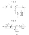
- FIG. 2 represents the block diagram of a first example of application of the amplifier according to the invention, to compensate for the accidental losses of a link L at long distance.
- An optical amplifier A n + 1 with adjustable gain and constant bandwidth makes it possible to compensate for an increase in losses in this link L.
- This link L comprises n amplifiers A 1 , ..., A n , with fixed gain, transmitting a plurality of spectrally multiplexed optical signals, referenced ⁇ i.
- the amplifier A n + 1 a an input connected to the output S of the link L, and an output coupled to a device U user of the useful optical signals, via an optical coupler CP.
- the coupler CP takes a fraction of the optical signals supplied by the output of the amplifier A n + 1 and supplies it to the input of a bandpass filter FPB, the passband of which constitutes the noise measurement band BB which is located outside the band BS of the useful signals.
- the output of the FPB filter is connected to an input of an MP device to measure the average power of the noise signal supplied by the filter.
- the MP device subtracts this average power from a reference value Ref corresponding to the nominal losses of the link L, and supplies a signal of average and nominal value Ref.
- the control signal supplied by the output of the MP device is applied to a gain control input of the amplifier A n + 1 , to adjust its gain so as to reduce the difference between the average noise power and the nominal value Ref .
- FIG. 3 represents the block diagram of a second example of application of the amplifier according to the invention. Similar elements have the same references as in Figure 2 with the prime attribute.
- the filter used is a band-rejecting FR filter, and more precisely reflecting towards its input the signals which it rejects.
- the rejected band is in this case the noise measurement band BB.
- a coupler CP 'and the filter FR are inserted in this order, between the output of the amplifier A' n + 1 and a user device U.
- the FR filter comprises a Bragg grating etched on an optical fiber.
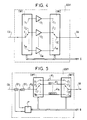
- the amplifiers G 1 , G 2 , .., G m thus respectively connect the outputs S 1 , S 2 , ..., S m to the inputs E 1 , E 2 , ..., E m .
- the structure of the switch SW1 is such that the outputs S 1 , S 2 , ..., S m are respectively connected to the input E when the binary word G takes respectively the values 1,2,3, ..., m .
- the structure of the switch SW2 is such that the inputs E 1 , E 2 , ..., E m are respectively connected to the output SC when the binary word G takes respectively the values 1,2, ..., m .
- the optical multiplex is amplified by the amplifier Gi, with the fixed gain corresponding to this amplifier, and with the same bandwidth whatever the selected amplifier.
- the amplifiers G 1 , ..., G m can be doped fiber or semiconductor amplifiers.
- the fiber section A ' 0 constitutes a preamplifier placed upstream of the battery of amplifiers constituted by the fiber sections A' 1 , A ' 2 , ..., A' m . It provides a gain equal to approximately half of the maximum gain of the AVG1 'amplifier.
- the gain of this preamplifier A ' 0 makes it possible to avoid that the insertion losses of the switch SW' 1 have an influence on the noise factor of the amplifier AVG1 '.
- the coupler CO ' 1 makes it possible to apply, in a codirectional manner, the pumping energy both to the fiber section A 0 , and to that of the fiber sections A' 1 , A ' 2 , ...., A ' m which is in service at the moment considered.
- the coupler CO ' 2 makes it possible to control the gain of the amplifier AVG1', according to the method described in French patent application No. 2,714,982, so that it has exactly the value represented by the binary word G.
- the fiber section A " 0 constitutes a preamplifier placed upstream of the amplifier bank made up of the fiber sections A" 1 , A “ 2 , ..., A” m . It provides a gain equal to approximately half of the maximum gain of the AVG1 "amplifier. The gain of this preamplifier A" 0 makes it possible to prevent the insertion losses of the switch SW “ 1 from having an influence on the noise factor AVG1 "amplifier.
- the CO “ 1 coupler allows pumping energy to be applied both to the fiber section A" 0 and to that of the fiber sections A “ 1 , A" 2 , ..., A " m which is in service at the time considered.
- the CO coupler " 2 makes it possible to control the gain of the amplifier AVG1", according to the method described in the French patent application No. 2,714,982, so that it has exactly the value represented by the binary word G.
- the amplifiers G 1 , ..., G m can be doped fiber or semiconductor. When it comes to semiconductor amplifiers they are activated or deactivated respectively by supplying or cutting their electrical supply.
- the preamplifier G 0 has a similar structure: a fiber section B 0 , an optical pump P 0 , and a coupler C 0 .
- the circuit CA activates a single amplifier selected from G 1 , ..., G m according to the value of the binary word G, which is between 1 and m. It selects the amplifier G i when this value is i. It permanently activates the G 0 preamplifier. It controls the gain of the set G 0 -G i by comparing the power of the amplified spontaneous emission to a set value which can be different for the different values of the gain control word G.
- the scope of the invention is not limited to the exemplary embodiments described above.
- the pumping of the amplifying fibers can be either co-directional, or cross-directional, or both.
Landscapes
- Engineering & Computer Science (AREA)
- Computer Networks & Wireless Communication (AREA)
- Signal Processing (AREA)
- Physics & Mathematics (AREA)
- Electromagnetism (AREA)
- Lasers (AREA)
- Optical Communication System (AREA)
- Control Of Amplification And Gain Control (AREA)
Applications Claiming Priority (2)
| Application Number | Priority Date | Filing Date | Title |
|---|---|---|---|
| FR9604668A FR2747483B1 (fr) | 1996-04-15 | 1996-04-15 | Amplificateur optique a gain variable et a bande passante constante, et systeme de compensation automatique des variations des pertes dans une liaison optique, comportant un tel amplificateur |
| FR9604668 | 1996-04-15 |
Publications (2)
| Publication Number | Publication Date |
|---|---|
| EP0802645A1 true EP0802645A1 (de) | 1997-10-22 |
| EP0802645B1 EP0802645B1 (de) | 2000-09-20 |
Family
ID=9491191
Family Applications (1)
| Application Number | Title | Priority Date | Filing Date |
|---|---|---|---|
| EP97400841A Expired - Lifetime EP0802645B1 (de) | 1996-04-15 | 1997-04-14 | Optischer Verstärker mit variabler Verstärkung und konstantem Durchlassband und automatisches Verluständerungenkompensationssystem in einer optischen Verbindung mit einem solchen Verstärker |
Country Status (8)
| Country | Link |
|---|---|
| US (1) | US6069731A (de) |
| EP (1) | EP0802645B1 (de) |
| JP (1) | JPH11509070A (de) |
| CA (1) | CA2222268A1 (de) |
| DE (1) | DE69703134T2 (de) |
| ES (1) | ES2150745T3 (de) |
| FR (1) | FR2747483B1 (de) |
| WO (1) | WO1997039547A1 (de) |
Cited By (2)
| Publication number | Priority date | Publication date | Assignee | Title |
|---|---|---|---|---|
| EP1139588A3 (de) * | 2000-03-29 | 2003-12-17 | Hitachi, Ltd. | Optisches Übertragungsgerät und Überwachungssystem dafür |
| EP1033834A3 (de) * | 1999-03-02 | 2003-12-17 | Fujitsu Limited | Optischer Verstärker und Optisches Übertragungssystem für Wellenlängenmultiplexübertragung |
Families Citing this family (19)
| Publication number | Priority date | Publication date | Assignee | Title |
|---|---|---|---|---|
| DE69836670T2 (de) * | 1997-10-28 | 2007-10-04 | Nec Corp. | Optischer Ein-/Ausfügemultiplexer |
| DE19838788A1 (de) * | 1998-08-26 | 2000-03-09 | Siemens Ag | Geregelter optischer Verstärker |
| US6785472B1 (en) * | 1999-06-15 | 2004-08-31 | Lucent Technologies Inc. | Broadband amplified WDM ring |
| US6424457B1 (en) * | 2000-10-06 | 2002-07-23 | Onetta, Inc. | Optical amplifiers and methods for manufacturing optical amplifiers |
| US6417964B1 (en) * | 2001-02-05 | 2002-07-09 | Avamex Corporation | Reconfigurable automatic gain control and method for optical amplifier |
| US6671085B2 (en) * | 2001-04-11 | 2003-12-30 | Bti Photonics Inc. | Switchable dynamic gain-flattened optical amplifiers and methods with wide dynamic gain range |
| US6943937B2 (en) * | 2001-05-17 | 2005-09-13 | Avanex Corporation | Optical amplifier performance controller and method of use |
| US7620331B2 (en) * | 2004-03-12 | 2009-11-17 | Finisar Corporation | Receiver circuit having an optical receiving device |
| US20050286119A1 (en) * | 2004-06-07 | 2005-12-29 | Wysocki Paul F | Article comprising a wideband optical amplifier with a wide dynamic range |
| JP2007078633A (ja) * | 2005-09-16 | 2007-03-29 | Seikoh Giken Co Ltd | 高感度3軸光電界センサ |
| JP4714535B2 (ja) * | 2005-09-21 | 2011-06-29 | 富士通株式会社 | 光増幅器 |
| JP4941017B2 (ja) * | 2007-03-09 | 2012-05-30 | 日本電気株式会社 | 光アンプ、その制御装置、制御回路、制御方法及び制御プログラム並びに光通信ネットワーク |
| CN101355388B (zh) * | 2007-07-25 | 2012-07-04 | 华为技术有限公司 | 接收装置和接收方法 |
| CN101719800B (zh) * | 2008-10-09 | 2013-10-30 | 昂纳信息技术(深圳)有限公司 | 一种提高放大器中信号功率和噪声功率比值的方法和装置 |
| JP5951601B2 (ja) * | 2011-05-24 | 2016-07-13 | 株式会社メガオプト | パルス光源 |
| US8873135B2 (en) * | 2012-12-21 | 2014-10-28 | Ciena Corporation | Extended dynamic range optical amplifier |
| JP6455297B2 (ja) * | 2015-04-24 | 2019-01-23 | 富士通株式会社 | 光増幅器、光伝送装置、及び光中継装置 |
| US10218454B2 (en) * | 2017-03-13 | 2019-02-26 | Google Llc | Open, modular, and scalable optical line system |
| CN116154592A (zh) * | 2023-02-28 | 2023-05-23 | 广东舜元激光科技有限公司 | 一种波形发生系统及其应用 |
Citations (2)
| Publication number | Priority date | Publication date | Assignee | Title |
|---|---|---|---|---|
| JPH0651355A (ja) * | 1992-07-31 | 1994-02-25 | Nec Corp | 光スイッチ |
| EP0655632A1 (de) * | 1993-11-16 | 1995-05-31 | AT&T Corp. | Optisches Filter mit integrierten Sendern/Empfängern |
Family Cites Families (5)
| Publication number | Priority date | Publication date | Assignee | Title |
|---|---|---|---|---|
| GB9305977D0 (en) * | 1993-03-23 | 1993-05-12 | Northern Telecom Ltd | Transmission system incorporating optical amplifiers |
| US5392154A (en) * | 1994-03-30 | 1995-02-21 | Bell Communications Research, Inc. | Self-regulating multiwavelength optical amplifier module for scalable lightwave communications systems |
| JPH08278523A (ja) * | 1995-04-05 | 1996-10-22 | Hitachi Ltd | 光増幅装置 |
| US5889610A (en) * | 1996-12-31 | 1999-03-30 | Lucent Technologies Inc. | Optical protection switching system |
| US5815613A (en) * | 1996-12-31 | 1998-09-29 | Lucent Technologies Inc. | Optical switched distributor |
-
1996
- 1996-04-15 FR FR9604668A patent/FR2747483B1/fr not_active Expired - Fee Related
-
1997
- 1997-04-14 ES ES97400841T patent/ES2150745T3/es not_active Expired - Lifetime
- 1997-04-14 JP JP9536807A patent/JPH11509070A/ja not_active Withdrawn
- 1997-04-14 WO PCT/FR1997/000658 patent/WO1997039547A1/fr not_active Ceased
- 1997-04-14 US US08/952,703 patent/US6069731A/en not_active Expired - Lifetime
- 1997-04-14 CA CA002222268A patent/CA2222268A1/fr not_active Abandoned
- 1997-04-14 EP EP97400841A patent/EP0802645B1/de not_active Expired - Lifetime
- 1997-04-14 DE DE69703134T patent/DE69703134T2/de not_active Expired - Lifetime
Patent Citations (2)
| Publication number | Priority date | Publication date | Assignee | Title |
|---|---|---|---|---|
| JPH0651355A (ja) * | 1992-07-31 | 1994-02-25 | Nec Corp | 光スイッチ |
| EP0655632A1 (de) * | 1993-11-16 | 1995-05-31 | AT&T Corp. | Optisches Filter mit integrierten Sendern/Empfängern |
Non-Patent Citations (3)
| Title |
|---|
| ESKILDSEN L ET AL: "SELF-REGULATING WDM AMPLIFIER MODULE FOR SCALABLE LIGHTWAVE NETWORKS", IEEE PHOTONICS TECHNOLOGY LETTERS, vol. 6, no. 11, 1 November 1994 (1994-11-01), pages 1321 - 1323, XP000486188 * |
| HILL G R ET AL: "A TRANSPORT NETWORK LAYER BASED ON OPTICAL NETWORK ELEMENTS", JOURNAL OF LIGHTWAVE TECHNOLOGY, vol. 11, no. 5/06, 1 May 1993 (1993-05-01), pages 667 - 676, XP000396700 * |
| PATENT ABSTRACTS OF JAPAN vol. 018, no. 284 (P - 1745) 30 May 1994 (1994-05-30) * |
Cited By (3)
| Publication number | Priority date | Publication date | Assignee | Title |
|---|---|---|---|---|
| EP1033834A3 (de) * | 1999-03-02 | 2003-12-17 | Fujitsu Limited | Optischer Verstärker und Optisches Übertragungssystem für Wellenlängenmultiplexübertragung |
| EP1139588A3 (de) * | 2000-03-29 | 2003-12-17 | Hitachi, Ltd. | Optisches Übertragungsgerät und Überwachungssystem dafür |
| US6839164B2 (en) | 2000-03-29 | 2005-01-04 | Hitachi, Ltd. | Optical transmission equipment and supervisory system thereof |
Also Published As
| Publication number | Publication date |
|---|---|
| CA2222268A1 (fr) | 1997-10-23 |
| FR2747483A1 (fr) | 1997-10-17 |
| DE69703134D1 (de) | 2000-10-26 |
| EP0802645B1 (de) | 2000-09-20 |
| WO1997039547A1 (fr) | 1997-10-23 |
| US6069731A (en) | 2000-05-30 |
| ES2150745T3 (es) | 2000-12-01 |
| FR2747483B1 (fr) | 1998-05-15 |
| JPH11509070A (ja) | 1999-08-03 |
| DE69703134T2 (de) | 2001-05-17 |
Similar Documents
| Publication | Publication Date | Title |
|---|---|---|
| EP0802645B1 (de) | Optischer Verstärker mit variabler Verstärkung und konstantem Durchlassband und automatisches Verluständerungenkompensationssystem in einer optischen Verbindung mit einem solchen Verstärker | |
| EP0818894A2 (de) | Sender für optische Signale und optisches Übertragunssystem mit einem solchen Sender | |
| FR2774482A1 (fr) | Procede d'egalisation de gain, dispositif et systeme pour une utilisation dans la mise en oeuvre du procede | |
| EP0744797B1 (de) | Multiwellenlängenquelle | |
| FR2760581A1 (fr) | Emetteur optique multiplexe en longueur d'onde | |
| FR2759831A1 (fr) | Amplificateur a fibre optique et systeme de communication optique equipe de celui-ci | |
| US6606189B2 (en) | Light amplifier and light amplifying method | |
| FR2762170A1 (fr) | Dispositif d'amplification optique capable de detecter au moins un signal parmi des signaux optiques individuels | |
| FR2762733A1 (fr) | Systeme de commande d'amplification de signal optique | |
| EP0802640B1 (de) | Verfahren und Vorrichtung zur Verstärkung von aus Wellenlängenmultiplex aufbereiteten Kanälen | |
| US6970613B2 (en) | Optical receiver and optical transmission apparatus | |
| FR2756693A1 (fr) | Systeme de transmission multiplexee en longueur d'onde optique | |
| EP0783212A1 (de) | Verteilungssystem von optischen Signalen | |
| EP1011216B1 (de) | Faseroptisches Übertragungssystem mit einem Empfangsfilter, der abstimmbare Bandbreite hat | |
| CN1918829B (zh) | 光网络和用于它的放大器节点 | |
| EP1155524A1 (de) | Wdm-ringübertragungsvorrichtung mit verstärkten abzweigkanälen | |
| EP2282430B1 (de) | Vorrichtung zum Mehrwege-Abzweigen von WDM-Kanälen | |
| FR2769139A1 (fr) | Appareil d'amplificateur optique | |
| EP2007049B1 (de) | Vorrichtung zur Übertragung optischer Signale mit unterschiedlichen Datenraten | |
| JP3175687B2 (ja) | 波長多重信号光のレベル監視制御方法及び波長多重光送信端局装置並びに中継装置 | |
| EP0994585A1 (de) | Leistungsausgleich in einem wellenlängenmultiplexierten optischen Übertragungssystem mit mehreren Verstärkern | |
| CA2286391A1 (fr) | Procede et dispositif d'extraction et insertion de canal pour transmission optique a multiplexage de longueurs d'onde | |
| FR2923336A1 (fr) | Transmetteur accordable en longueurs d'onde et a filtrage integre pour un reseau de communication optique (d)wdm, et transpondeur correspondant | |
| EP1098465A1 (de) | Verfahren zum Abführen von einem Kanal für ein optisches Wellenlängemultiplex-Übertragungsystem und Vorrichtung zur Anwendung dieses Verfahrens |
Legal Events
| Date | Code | Title | Description |
|---|---|---|---|
| PUAI | Public reference made under article 153(3) epc to a published international application that has entered the european phase |
Free format text: ORIGINAL CODE: 0009012 |
|
| AK | Designated contracting states |
Kind code of ref document: A1 Designated state(s): DE ES FR GB IT SE |
|
| 17P | Request for examination filed |
Effective date: 19980303 |
|
| RAP3 | Party data changed (applicant data changed or rights of an application transferred) |
Owner name: ALCATEL |
|
| 17Q | First examination report despatched |
Effective date: 19990120 |
|
| GRAG | Despatch of communication of intention to grant |
Free format text: ORIGINAL CODE: EPIDOS AGRA |
|
| GRAG | Despatch of communication of intention to grant |
Free format text: ORIGINAL CODE: EPIDOS AGRA |
|
| GRAH | Despatch of communication of intention to grant a patent |
Free format text: ORIGINAL CODE: EPIDOS IGRA |
|
| RBV | Designated contracting states (corrected) |
Designated state(s): DE ES FR GB IT SE |
|
| GRAH | Despatch of communication of intention to grant a patent |
Free format text: ORIGINAL CODE: EPIDOS IGRA |
|
| GRAA | (expected) grant |
Free format text: ORIGINAL CODE: 0009210 |
|
| AK | Designated contracting states |
Kind code of ref document: B1 Designated state(s): DE ES FR GB IT SE |
|
| REF | Corresponds to: |
Ref document number: 69703134 Country of ref document: DE Date of ref document: 20001026 |
|
| GBT | Gb: translation of ep patent filed (gb section 77(6)(a)/1977) |
Effective date: 20001006 |
|
| ITF | It: translation for a ep patent filed | ||
| REG | Reference to a national code |
Ref country code: ES Ref legal event code: FG2A Ref document number: 2150745 Country of ref document: ES Kind code of ref document: T3 |
|
| PLBE | No opposition filed within time limit |
Free format text: ORIGINAL CODE: 0009261 |
|
| STAA | Information on the status of an ep patent application or granted ep patent |
Free format text: STATUS: NO OPPOSITION FILED WITHIN TIME LIMIT |
|
| 26N | No opposition filed | ||
| REG | Reference to a national code |
Ref country code: GB Ref legal event code: IF02 |
|
| PGFP | Annual fee paid to national office [announced via postgrant information from national office to epo] |
Ref country code: IT Payment date: 20060430 Year of fee payment: 10 |
|
| REG | Reference to a national code |
Ref country code: FR Ref legal event code: CD |
|
| PG25 | Lapsed in a contracting state [announced via postgrant information from national office to epo] |
Ref country code: IT Free format text: LAPSE BECAUSE OF NON-PAYMENT OF DUE FEES Effective date: 20070414 |
|
| PGFP | Annual fee paid to national office [announced via postgrant information from national office to epo] |
Ref country code: ES Payment date: 20120425 Year of fee payment: 16 |
|
| PGFP | Annual fee paid to national office [announced via postgrant information from national office to epo] |
Ref country code: GB Payment date: 20130418 Year of fee payment: 17 Ref country code: SE Payment date: 20130418 Year of fee payment: 17 Ref country code: DE Payment date: 20130419 Year of fee payment: 17 |
|
| PGFP | Annual fee paid to national office [announced via postgrant information from national office to epo] |
Ref country code: FR Payment date: 20130515 Year of fee payment: 17 |
|
| REG | Reference to a national code |
Ref country code: FR Ref legal event code: GC Effective date: 20140717 |
|
| REG | Reference to a national code |
Ref country code: DE Ref legal event code: R119 Ref document number: 69703134 Country of ref document: DE |
|
| REG | Reference to a national code |
Ref country code: FR Ref legal event code: RG Effective date: 20141016 |
|
| REG | Reference to a national code |
Ref country code: SE Ref legal event code: EUG |
|
| GBPC | Gb: european patent ceased through non-payment of renewal fee |
Effective date: 20140414 |
|
| REG | Reference to a national code |
Ref country code: FR Ref legal event code: ST Effective date: 20141231 |
|
| PG25 | Lapsed in a contracting state [announced via postgrant information from national office to epo] |
Ref country code: GB Free format text: LAPSE BECAUSE OF NON-PAYMENT OF DUE FEES Effective date: 20140414 Ref country code: DE Free format text: LAPSE BECAUSE OF NON-PAYMENT OF DUE FEES Effective date: 20141101 Ref country code: SE Free format text: LAPSE BECAUSE OF NON-PAYMENT OF DUE FEES Effective date: 20140415 |
|
| REG | Reference to a national code |
Ref country code: DE Ref legal event code: R119 Ref document number: 69703134 Country of ref document: DE Effective date: 20141101 |
|
| PG25 | Lapsed in a contracting state [announced via postgrant information from national office to epo] |
Ref country code: FR Free format text: LAPSE BECAUSE OF NON-PAYMENT OF DUE FEES Effective date: 20140430 |
|
| REG | Reference to a national code |
Ref country code: ES Ref legal event code: FD2A Effective date: 20150528 |
|
| PG25 | Lapsed in a contracting state [announced via postgrant information from national office to epo] |
Ref country code: ES Free format text: LAPSE BECAUSE OF NON-PAYMENT OF DUE FEES Effective date: 20140415 |