EP0803895A2 - Elektrode für Plasmaätzen - Google Patents
Elektrode für Plasmaätzen Download PDFInfo
- Publication number
- EP0803895A2 EP0803895A2 EP97302743A EP97302743A EP0803895A2 EP 0803895 A2 EP0803895 A2 EP 0803895A2 EP 97302743 A EP97302743 A EP 97302743A EP 97302743 A EP97302743 A EP 97302743A EP 0803895 A2 EP0803895 A2 EP 0803895A2
- Authority
- EP
- European Patent Office
- Prior art keywords
- electrode
- plasma etching
- glassy carbon
- surface side
- baffle plate
- Prior art date
- Legal status (The legal status is an assumption and is not a legal conclusion. Google has not performed a legal analysis and makes no representation as to the accuracy of the status listed.)
- Ceased
Links
- 238000001020 plasma etching Methods 0.000 title claims abstract description 21
- 229910021397 glassy carbon Inorganic materials 0.000 claims description 18
- 229910052710 silicon Inorganic materials 0.000 claims description 17
- 239000010703 silicon Substances 0.000 claims description 17
- 239000003575 carbonaceous material Substances 0.000 claims description 9
- 229910052751 metal Inorganic materials 0.000 claims description 8
- 239000002184 metal Substances 0.000 claims description 8
- 239000000428 dust Substances 0.000 abstract description 7
- XUIMIQQOPSSXEZ-UHFFFAOYSA-N Silicon Chemical compound [Si] XUIMIQQOPSSXEZ-UHFFFAOYSA-N 0.000 description 16
- 239000002245 particle Substances 0.000 description 9
- 238000005530 etching Methods 0.000 description 8
- 239000000463 material Substances 0.000 description 5
- 230000002159 abnormal effect Effects 0.000 description 4
- 238000003754 machining Methods 0.000 description 4
- 238000000034 method Methods 0.000 description 4
- 238000005553 drilling Methods 0.000 description 3
- XPFVYQJUAUNWIW-UHFFFAOYSA-N furfuryl alcohol Chemical compound OCC1=CC=CO1 XPFVYQJUAUNWIW-UHFFFAOYSA-N 0.000 description 3
- CSCPPACGZOOCGX-UHFFFAOYSA-N Acetone Chemical compound CC(C)=O CSCPPACGZOOCGX-UHFFFAOYSA-N 0.000 description 2
- XKRFYHLGVUSROY-UHFFFAOYSA-N Argon Chemical compound [Ar] XKRFYHLGVUSROY-UHFFFAOYSA-N 0.000 description 2
- OKTJSMMVPCPJKN-UHFFFAOYSA-N Carbon Chemical compound [C] OKTJSMMVPCPJKN-UHFFFAOYSA-N 0.000 description 2
- XPDWGBQVDMORPB-UHFFFAOYSA-N Fluoroform Chemical compound FC(F)F XPDWGBQVDMORPB-UHFFFAOYSA-N 0.000 description 2
- 229910052782 aluminium Inorganic materials 0.000 description 2
- XAGFODPZIPBFFR-UHFFFAOYSA-N aluminium Chemical compound [Al] XAGFODPZIPBFFR-UHFFFAOYSA-N 0.000 description 2
- 238000005336 cracking Methods 0.000 description 2
- 229910002804 graphite Inorganic materials 0.000 description 2
- 239000010439 graphite Substances 0.000 description 2
- 238000005498 polishing Methods 0.000 description 2
- 239000012495 reaction gas Substances 0.000 description 2
- 229920005989 resin Polymers 0.000 description 2
- 239000011347 resin Substances 0.000 description 2
- 239000004065 semiconductor Substances 0.000 description 2
- ZOXJGFHDIHLPTG-UHFFFAOYSA-N Boron Chemical compound [B] ZOXJGFHDIHLPTG-UHFFFAOYSA-N 0.000 description 1
- 239000003082 abrasive agent Substances 0.000 description 1
- 229910052786 argon Inorganic materials 0.000 description 1
- QVGXLLKOCUKJST-UHFFFAOYSA-N atomic oxygen Chemical compound [O] QVGXLLKOCUKJST-UHFFFAOYSA-N 0.000 description 1
- 229910052796 boron Inorganic materials 0.000 description 1
- 229920002678 cellulose Polymers 0.000 description 1
- 239000001913 cellulose Substances 0.000 description 1
- 230000000052 comparative effect Effects 0.000 description 1
- 239000013078 crystal Substances 0.000 description 1
- 239000007849 furan resin Substances 0.000 description 1
- 229920005546 furfural resin Polymers 0.000 description 1
- 239000007789 gas Substances 0.000 description 1
- 239000012535 impurity Substances 0.000 description 1
- 238000004519 manufacturing process Methods 0.000 description 1
- 239000000203 mixture Substances 0.000 description 1
- 229910021421 monocrystalline silicon Inorganic materials 0.000 description 1
- 230000003287 optical effect Effects 0.000 description 1
- 239000001301 oxygen Substances 0.000 description 1
- 229910052760 oxygen Inorganic materials 0.000 description 1
- 239000005011 phenolic resin Substances 0.000 description 1
- 239000010453 quartz Substances 0.000 description 1
- VYPSYNLAJGMNEJ-UHFFFAOYSA-N silicon dioxide Inorganic materials O=[Si]=O VYPSYNLAJGMNEJ-UHFFFAOYSA-N 0.000 description 1
- 229920001187 thermosetting polymer Polymers 0.000 description 1
- XLYOFNOQVPJJNP-UHFFFAOYSA-N water Substances O XLYOFNOQVPJJNP-UHFFFAOYSA-N 0.000 description 1
Images

Classifications
-
- H—ELECTRICITY
- H01—ELECTRIC ELEMENTS
- H01J—ELECTRIC DISCHARGE TUBES OR DISCHARGE LAMPS
- H01J37/00—Discharge tubes with provision for introducing objects or material to be exposed to the discharge, e.g. for the purpose of examination or processing thereof
- H01J37/32—Gas-filled discharge tubes
- H01J37/32431—Constructional details of the reactor
- H01J37/32532—Electrodes
- H01J37/32541—Shape
Definitions
- the present invention relates to an electrode for parallel plate electrode type plasma etching , e.g. as used for production of semiconductor integrated circuits, such as LSIs or ICs, or waveguides for optical communication.
- preferred embodiments of the present invention may provide an electrode for parallel plate type plasma etching, which is capable of significantly reducing the generation of dust.
- an electrode for parallel plate type plasma etching which is capable of suppressing the generation of particles during etching and enabling high precise plasma etching at high yield, can be obtained by specifying a flatness (defined in JIS-B0021) of the electrode to be in a range of from 0.001 to 5 mm, and preferably ⁇ 4mm and specifying a camber of the electrode such that the front surface side of the electrode is recessed and the back surface side thereof projects.
- the present inventor has examined how particles (dust) are generated from an etching electrode, and found that other than a known mechanism that particles are generated from the electrode when the electrode is bombarded with plasma, there is another mechanism that when a gap is formed between a member (called a baffle plate) provided on the back surface of an etching electrode and the etching electrode, an abnormal discharge is possibly generated in the gap, so that dust particles are generated by the abnormal discharge.
- a baffle plate a member
- the generation of dust can be prevented or reduced by specifying a flatness (defined in JIS-B0021) of the electrode to be in a range of from 0.001 to 5mm, and preferably, specifying a camber direction of the electrode such that the front surface side of the electrode is recessed and the back surface side thereof projects, whereby closely mounting the plasma etching electrode on the baffle plate without any gap.
- a flatness defined in JIS-B0021
- a camber direction of the electrode such that the front surface side of the electrode is recessed and the back surface side thereof projects
- an electrode for parallel plate electrode type plasma etching which has a flatness in a range of from 0.001 to 5 mm, and preferably, which has such a camber that the front surface side of the electrode is recessed and the back surface side thereof projects. Additionally, the above electrode is preferably configured that at least a portion of the electrode to be consumed by plasma is formed of a glassy carbon material or metal silicon.
- An electrode for parallel flat type plasma etching according to the present invention has a flatness (defined in JIS B0021), that is, the cambered amount in a range of from 0.001 to 5 mm, preferably, in a range of from 0.001 to 2 mm.
- a flatness defined in JIS B0021
- the cambered amount in a range of from 0.001 to 5 mm, preferably, in a range of from 0.001 to 2 mm.
- the electrode preferably has such a camber that the front surface side of the electrode is recessed and the back surface side thereof projects.
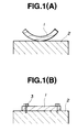
- Figs. 1(A), 1(B) and Figs. 2(A), 2(B) in the case where an electrode 1 is mounted on a baffle plate 2, assuming that the camber direction where the projecting surface of the electrode 1 is brought in press-contact with the baffle plate provided on the back surface side is specified as a positive direction and that a camber direction where the recessed surface of the electrode is brought in press-contact with the baffle plate 2 is specified as a negative direction, it is desired that the electrode 1 is cambered in the positive direction.
- the electrode may be formed of a known material, but to achieve the object of the present invention, it is preferably formed of metal silicon or a glassy carbon material.
- the glassy carbon material may be produced from a source material selected from cellulose, furfuryl alcohol, phenol resin, acetone, polycarbodiimide resin, furan resin, furfural resin, other thermosetting resins, and mixtures thereof.
- Metal silicon may be of either a single crystal type or a polycrystalline type.
- the entire electrode may be formed of metal silicon or a glassy carbon material.
- at least a portion to be consumed by plasma may be formed of metal silicon or a glassy carbon material.
- a portion other than the portion formed of metal silicon or a glassy carbon material can be formed of aluminum or graphite, although in terms of the material cost, it is preferably formed of a carbon material covered with a glassy carbon material.
- the surface, particularly, the surface to be in contact with plasma can be polished by, for example, lapping using abrasives, buffing, or electrolytic polishing.
- the plasma etching electrode of the present invention can be formed with a suitable number of through-holes for allowing a reaction gas to smoothly flow in a plasma region therethrough.
- a through-hole can be formed by ultrasonic machining, electric discharge machining, drilling, laser machining, or water jet machining.
- the plasma etching electrode of the present invention is most suitable for parallel flat type plasma etching, but it can be used for a general plasma etching process; and the plasma etching using such an electrode can be performed under normal conditions.
- An electrode sample having a flatness and a camber direction shown in Table 1 was prepared by slicing a single crystal silicon member doped with P-type boron into a thickness of 4 mm, forming holes (diameter: 0.8 mm, pitch: 3.175 mm) in the surface of the member by drilling, and polishing the surface of the member using a lapping machine.
- An electrode sample having a flatness and a camber direction shown in Table 1 was also prepared by drilling and surface-finishing a glassy carbon plate (concentration of impurity: 2 ppm, thickness: 4 mm) in the same manner as described above.
- Each of the above electrode samples was mounted on a baffle plate and set into a plasma etching system, and an oxide film on a silicon wafer (diameter: 6 inch (15cm)) was etched by plasma using a mixed gas of trifluoromethane as a reaction gas, argon and oxygen. After this etching, the number of particles (particle size: 0.3 ⁇ m or more) adhering on the surface of the wafer was counted. The results were shown in Table 1.
- a plasma etching electrode according to the present invention can significantly reduce the number of particles at the etching step and enables high precise etching at a high yield.
- Table 1 material camber direction flatness number of particles Example 1 silicon + 0.001 1 2 silicon + 0.05 1 3 silicon + 0.1 1 4 silicon + 0.5 2 5 silicon + 1.9 2 6 glassy carbon + 0.001 3 7 glassy carbon + 0.05 4 8 glassy carbon + 0.12 3 9 glassy carbon + 0.6 4 10 glassy carbon + 1.9 5 Comparative Example 1 silicon - 0.1 30 2 silicon - 1 80 3 silicon + 5 *1) 4 glassy carbon - 0.1 28 5 glassy carbon - 1.3 100 6 glassy carbon + 5 *2) *1,2) cracking of electrode upon mounting on baffle plate
Landscapes
- Physics & Mathematics (AREA)
- Engineering & Computer Science (AREA)
- Plasma & Fusion (AREA)
- Chemical & Material Sciences (AREA)
- Analytical Chemistry (AREA)
- ing And Chemical Polishing (AREA)
- Drying Of Semiconductors (AREA)
- Gas-Filled Discharge Tubes (AREA)
Applications Claiming Priority (2)
| Application Number | Priority Date | Filing Date | Title |
|---|---|---|---|
| JP8124073A JPH09289196A (ja) | 1996-04-22 | 1996-04-22 | プラズマエッチング電極 |
| JP124073/96 | 1996-04-22 |
Publications (2)
| Publication Number | Publication Date |
|---|---|
| EP0803895A2 true EP0803895A2 (de) | 1997-10-29 |
| EP0803895A3 EP0803895A3 (de) | 1998-04-01 |
Family
ID=14876274
Family Applications (1)
| Application Number | Title | Priority Date | Filing Date |
|---|---|---|---|
| EP97302743A Ceased EP0803895A3 (de) | 1996-04-22 | 1997-04-22 | Elektrode für Plasmaätzen |
Country Status (5)
| Country | Link |
|---|---|
| US (1) | US6007672A (de) |
| EP (1) | EP0803895A3 (de) |
| JP (1) | JPH09289196A (de) |
| KR (1) | KR970070242A (de) |
| TW (1) | TW349131B (de) |
Cited By (1)
| Publication number | Priority date | Publication date | Assignee | Title |
|---|---|---|---|---|
| EP0795889A3 (de) * | 1996-02-15 | 1998-06-10 | Tokai Carbon Company Ltd. | Elektrodenscheibe für Plasma-Ätzvorrichtung |
Families Citing this family (4)
| Publication number | Priority date | Publication date | Assignee | Title |
|---|---|---|---|---|
| JP3990867B2 (ja) * | 2000-01-31 | 2007-10-17 | キヤノン株式会社 | 堆積膜形成装置および堆積膜形成方法 |
| US6638359B2 (en) * | 2000-01-31 | 2003-10-28 | Canon Kabushiki Kaisha | Deposited film forming apparatus and deposited film forming method |
| US6576202B1 (en) * | 2000-04-21 | 2003-06-10 | Kin-Chung Ray Chiu | Highly efficient compact capacitance coupled plasma reactor/generator and method |
| TWI319610B (en) * | 2006-12-29 | 2010-01-11 | Winbond Electronics Corp | Method of manufacturing openings and via openings |
Citations (5)
| Publication number | Priority date | Publication date | Assignee | Title |
|---|---|---|---|---|
| US4132614A (en) * | 1977-10-26 | 1979-01-02 | International Business Machines Corporation | Etching by sputtering from an intermetallic target to form negative metallic ions which produce etching of a juxtaposed substrate |
| US5066381A (en) * | 1988-04-15 | 1991-11-19 | Sharp Kabushiki Kaisha | Target unit |
| US5074456A (en) * | 1990-09-18 | 1991-12-24 | Lam Research Corporation | Composite electrode for plasma processes |
| JPH06128762A (ja) * | 1992-10-21 | 1994-05-10 | Hitachi Chem Co Ltd | プラズマエッチング用電極板 |
| EP0795889A2 (de) * | 1996-02-15 | 1997-09-17 | Tokai Carbon Company Ltd. | Elektrodenscheibe für Plasma-Ätzvorrichtung |
Family Cites Families (7)
| Publication number | Priority date | Publication date | Assignee | Title |
|---|---|---|---|---|
| JPS61206225A (ja) * | 1985-03-11 | 1986-09-12 | Hitachi Ltd | 温度制御装置 |
| JPS63131518A (ja) * | 1986-11-21 | 1988-06-03 | Toshiba Corp | ドライエツチング装置 |
| EP0290093A1 (de) * | 1987-05-07 | 1988-11-09 | Koninklijke Philips Electronics N.V. | Mit einer Flüssigkeit gefüllte elektroskopische Anzeigevorrichtung und Herstellungsverfahren |
| JPH07114198B2 (ja) * | 1989-10-02 | 1995-12-06 | 東海カーボン株式会社 | プラズマエッチング用電極板 |
| JPH0629249A (ja) * | 1991-10-08 | 1994-02-04 | Ulvac Japan Ltd | プラズマエッチング装置 |
| US5252196A (en) * | 1991-12-05 | 1993-10-12 | Shipley Company Inc. | Copper electroplating solutions and processes |
| US5681195A (en) * | 1993-09-30 | 1997-10-28 | Matsushita Electric Industrial Co., Ltd. | Flat display device and manufacturing method thereof |
-
1996
- 1996-04-22 JP JP8124073A patent/JPH09289196A/ja active Pending
-
1997
- 1997-04-17 TW TW086104968A patent/TW349131B/zh active
- 1997-04-18 US US08/839,366 patent/US6007672A/en not_active Expired - Lifetime
- 1997-04-22 KR KR1019970014840A patent/KR970070242A/ko not_active Ceased
- 1997-04-22 EP EP97302743A patent/EP0803895A3/de not_active Ceased
Patent Citations (5)
| Publication number | Priority date | Publication date | Assignee | Title |
|---|---|---|---|---|
| US4132614A (en) * | 1977-10-26 | 1979-01-02 | International Business Machines Corporation | Etching by sputtering from an intermetallic target to form negative metallic ions which produce etching of a juxtaposed substrate |
| US5066381A (en) * | 1988-04-15 | 1991-11-19 | Sharp Kabushiki Kaisha | Target unit |
| US5074456A (en) * | 1990-09-18 | 1991-12-24 | Lam Research Corporation | Composite electrode for plasma processes |
| JPH06128762A (ja) * | 1992-10-21 | 1994-05-10 | Hitachi Chem Co Ltd | プラズマエッチング用電極板 |
| EP0795889A2 (de) * | 1996-02-15 | 1997-09-17 | Tokai Carbon Company Ltd. | Elektrodenscheibe für Plasma-Ätzvorrichtung |
Non-Patent Citations (4)
| Title |
|---|
| JIS B 0021 (item 18, fIg. 62 and 63) & English translation * |
| Klein, Einführung in die DIN-Normen, Teubner 1985 (pages 306-309) * |
| PATENT ABSTRACTS OF JAPAN vol. 018, no. 430 (C - 1236) 11 August 1994 (1994-08-11) * |
| S.M. Sze, VLSI Technology, 2nd Edition, McGraw Hill 1988 * |
Cited By (1)
| Publication number | Priority date | Publication date | Assignee | Title |
|---|---|---|---|---|
| EP0795889A3 (de) * | 1996-02-15 | 1998-06-10 | Tokai Carbon Company Ltd. | Elektrodenscheibe für Plasma-Ätzvorrichtung |
Also Published As
| Publication number | Publication date |
|---|---|
| EP0803895A3 (de) | 1998-04-01 |
| US6007672A (en) | 1999-12-28 |
| TW349131B (en) | 1999-01-01 |
| JPH09289196A (ja) | 1997-11-04 |
| KR970070242A (ko) | 1997-11-07 |
Similar Documents
| Publication | Publication Date | Title |
|---|---|---|
| EP0803897A2 (de) | Elektrode für Plasmaätzen | |
| EP1081749B1 (de) | Schutzelement für die innere oberfläche einer kammer und plasmabehandlungsvorrichtung | |
| US7646581B2 (en) | Electrostatic chuck | |
| US5993597A (en) | Plasma etching electrode | |
| KR20060043193A (ko) | 플라즈마 처리장치 및 플라즈마 처리방법 | |
| JP4905855B2 (ja) | プラズマエッチング用フォーカスリングおよびシールドリング | |
| EP0803895A2 (de) | Elektrode für Plasmaätzen | |
| CN100382230C (zh) | 硅电极及其生产方法、生产硅部件及加工半导体晶片方法 | |
| EP0803896B1 (de) | Plasmabehandlungsvorrichtung und Schutzteil dafür | |
| EP0743677A2 (de) | Blindscheibe | |
| JP3444089B2 (ja) | プラズマエッチング電極 | |
| JP2000049144A (ja) | プラズマ処理装置用電極板 | |
| JPH11281307A (ja) | 電極板、電極板の製造方法およびその小径孔内壁表面粗さの測定方法 | |
| JPH09289195A (ja) | プラズマエッチング電極 | |
| JPH06128762A (ja) | プラズマエッチング用電極板 | |
| US7344652B2 (en) | Plasma etching method | |
| JP2000306886A (ja) | プラズマエッチング電極 | |
| EP0663687B1 (de) | Vorrichtung und Verfahren zur Herstellung von Halbleitern | |
| JPH09289199A (ja) | プラズマエッチング電極 | |
| EP0600365A1 (de) | Elektrode zum Einsatz beim Plasmaätzen | |
| JPH08134667A (ja) | プラズマエッチング用陽極電極板 | |
| JPH07273094A (ja) | プラズマエッチング用電極板 | |
| JPH1022275A (ja) | プラズマエッチング電極の製造方法 | |
| EP0795889A2 (de) | Elektrodenscheibe für Plasma-Ätzvorrichtung | |
| KR19980076734A (ko) | 플라즈마 처리 장치 |
Legal Events
| Date | Code | Title | Description |
|---|---|---|---|
| PUAI | Public reference made under article 153(3) epc to a published international application that has entered the european phase |
Free format text: ORIGINAL CODE: 0009012 |
|
| AK | Designated contracting states |
Kind code of ref document: A2 Designated state(s): DE FR GB |
|
| PUAL | Search report despatched |
Free format text: ORIGINAL CODE: 0009013 |
|
| AK | Designated contracting states |
Kind code of ref document: A3 Designated state(s): DE FR GB |
|
| 17P | Request for examination filed |
Effective date: 19980429 |
|
| 17Q | First examination report despatched |
Effective date: 19991214 |
|
| STAA | Information on the status of an ep patent application or granted ep patent |
Free format text: STATUS: THE APPLICATION HAS BEEN REFUSED |
|
| 18R | Application refused |
Effective date: 20010419 |