EP0807925A1 - Magnetkopf mit unter der Spalte angeordnetem Halbleiterfelddetektor - Google Patents
Magnetkopf mit unter der Spalte angeordnetem Halbleiterfelddetektor Download PDFInfo
- Publication number
- EP0807925A1 EP0807925A1 EP97400867A EP97400867A EP0807925A1 EP 0807925 A1 EP0807925 A1 EP 0807925A1 EP 97400867 A EP97400867 A EP 97400867A EP 97400867 A EP97400867 A EP 97400867A EP 0807925 A1 EP0807925 A1 EP 0807925A1
- Authority
- EP
- European Patent Office
- Prior art keywords
- detector
- magnetic
- air gap
- magnetic head
- current
- Prior art date
- Legal status (The legal status is an assumption and is not a legal conclusion. Google has not performed a legal analysis and makes no representation as to the accuracy of the status listed.)
- Withdrawn
Links
- 239000004065 semiconductor Substances 0.000 title claims abstract description 20
- 230000010287 polarization Effects 0.000 claims description 4
- 230000004907 flux Effects 0.000 abstract description 6
- 238000004804 winding Methods 0.000 abstract description 4
- 229910001030 Iron–nickel alloy Inorganic materials 0.000 abstract 1
- 239000010409 thin film Substances 0.000 abstract 1
- 230000005355 Hall effect Effects 0.000 description 4
- XUIMIQQOPSSXEZ-UHFFFAOYSA-N Silicon Chemical compound [Si] XUIMIQQOPSSXEZ-UHFFFAOYSA-N 0.000 description 2
- 230000003321 amplification Effects 0.000 description 2
- 238000005259 measurement Methods 0.000 description 2
- 238000003199 nucleic acid amplification method Methods 0.000 description 2
- 229910052710 silicon Inorganic materials 0.000 description 2
- 239000010703 silicon Substances 0.000 description 2
- 230000000903 blocking effect Effects 0.000 description 1
- 238000001514 detection method Methods 0.000 description 1
- UGKDIUIOSMUOAW-UHFFFAOYSA-N iron nickel Chemical compound [Fe].[Ni] UGKDIUIOSMUOAW-UHFFFAOYSA-N 0.000 description 1
- 229920006395 saturated elastomer Polymers 0.000 description 1
- 238000000926 separation method Methods 0.000 description 1
- 239000000758 substrate Substances 0.000 description 1
Images


Classifications
-
- G—PHYSICS
- G11—INFORMATION STORAGE
- G11B—INFORMATION STORAGE BASED ON RELATIVE MOVEMENT BETWEEN RECORD CARRIER AND TRANSDUCER
- G11B5/00—Recording by magnetisation or demagnetisation of a record carrier; Reproducing by magnetic means; Record carriers therefor
- G11B5/127—Structure or manufacture of heads, e.g. inductive
- G11B5/33—Structure or manufacture of flux-sensitive heads, i.e. for reproduction only; Combination of such heads with means for recording or erasing only
- G11B5/37—Structure or manufacture of flux-sensitive heads, i.e. for reproduction only; Combination of such heads with means for recording or erasing only using galvano-magnetic devices, e.g. Hall-effect devices using Hall or Hall-related effect, e.g. planar-Hall effect or pseudo-Hall effect
- G11B5/376—Structure or manufacture of flux-sensitive heads, i.e. for reproduction only; Combination of such heads with means for recording or erasing only using galvano-magnetic devices, e.g. Hall-effect devices using Hall or Hall-related effect, e.g. planar-Hall effect or pseudo-Hall effect in semi-conductors
- G11B5/378—Integrated structures
-
- G—PHYSICS
- G11—INFORMATION STORAGE
- G11B—INFORMATION STORAGE BASED ON RELATIVE MOVEMENT BETWEEN RECORD CARRIER AND TRANSDUCER
- G11B5/00—Recording by magnetisation or demagnetisation of a record carrier; Reproducing by magnetic means; Record carriers therefor
- G11B5/127—Structure or manufacture of heads, e.g. inductive
- G11B5/33—Structure or manufacture of flux-sensitive heads, i.e. for reproduction only; Combination of such heads with means for recording or erasing only
-
- G—PHYSICS
- G11—INFORMATION STORAGE
- G11B—INFORMATION STORAGE BASED ON RELATIVE MOVEMENT BETWEEN RECORD CARRIER AND TRANSDUCER
- G11B5/00—Recording by magnetisation or demagnetisation of a record carrier; Reproducing by magnetic means; Record carriers therefor
- G11B5/127—Structure or manufacture of heads, e.g. inductive
- G11B5/33—Structure or manufacture of flux-sensitive heads, i.e. for reproduction only; Combination of such heads with means for recording or erasing only
- G11B5/37—Structure or manufacture of flux-sensitive heads, i.e. for reproduction only; Combination of such heads with means for recording or erasing only using galvano-magnetic devices, e.g. Hall-effect devices using Hall or Hall-related effect, e.g. planar-Hall effect or pseudo-Hall effect
Definitions
- the present invention relates to a magnetic head with a semiconductor field detector placed under the air gap.
- the invention finds an application in the recording of information on disc, tape, etc.
- a magnetic field detector head generally comprises, as shown in the appended FIG. 1, a semiconductor substrate 12, a lower magnetic part 14, two magnetic pillars 16 1 , 16 2 , a conductive winding 18, two flux concentrators 20 1 , 20 2 and two pole pieces 22 1 , 22 2 separated by an air gap 24.
- the detector for measuring the reading field can be placed in an air gap dividing the lower magnetic piece 14, as described in French patent FR-A- 2,700,633 or at intervals in the pillars. However, it may be preferable to place it between one of the concentrators 20 1 , 20 2 and one of the pole pieces 22 1 , 22 2 , as shown in the figure where it bears the reference 30. Being placed closer to the air gap 24, the detector receives more magnetic flux and is therefore more efficient.
- the present invention aims precisely to solve this problem and aims all the same the semiconductor detector under the gap to benefit from better efficiency.
- the invention first proposes to use a semiconductor detector of a particular type.
- a semiconductor detector for example with HALL effect, consists of suitable semiconductor layers traversed by a so-called bias current.
- the device For a detector operating in voltage, the device has a square shape. Current is injected between two opposite sides of the square and the voltage is drawn between the other two opposite sides of the square. This voltage is proportional to the product of the bias current by the component of the magnetic field perpendicular to the plane of the layers.
- the read signal would be zero, for the reasons indicated above.
- the invention recommends the use of another type of detector, operating in current and no longer in voltage, and which has an elongated shape with two symmetrical parts. If these two parts are placed under the two pole pieces, symmetrically with respect to the median plane of the air gap, and if the detector operates as usual, the current delivered remains zero. But if we reverse the bias current in one of the two parts, the measurement signal is no longer zero and takes a value proportional to the absolute value of the vertical component of the magnetic field.
- the present invention therefore relates to a magnetic head comprising a magnetic circuit with two pole pieces separated by an air gap and a semiconductor magnetic field detector, characterized in that this detector is placed under the air gap and comprises two elongated symmetrical parts arranged under the pole pieces and traversed by equal polarization currents but opposite in direction.
- the two parts of the detector can be supplied separately by two polarization sources, it seems simpler to supply them in series by the same source. It then suffices to link one of the parts to the other.
- the detector also comprises a thin magnetic layer intended to channel the magnetic field.
- HALL detectors appear to be the most advantageous.
- FIG 2 the part of the magnetic head located around the air gap.
- the magnetic field lines under the air gap are represented schematically by the arrowed lines 36. These lines are supposed to start from the pole piece 22 1 and end up on the pole piece 22 2 .
- the field is therefore substantially directed downwards under the first pole piece and upwards under the second.
- the field is horizontal in the plane of symmetry of the air gap.
- FIG. 3 shows an elongated HALL effect detector used in accordance with the invention.
- a detector comprises suitable semiconductor layers 42 etched in the form of a rectangle and a double pair of electrical contacts for current input and output, namely the contacts 44a and 44b for the input and 44c and 44d for the output.
- a current loop 46 placed on any one of the four input or output connections, delivers a voltage V sensitive not to the bias current, which is continuous, but at its variation Ih / 2.
- the voltage V across the loop therefore constitutes the measurement signal.
- the polarization current is reversed in one of the two parts of the detector, for example in the right part according to the representation in FIG. 8.
- the current lines then tilt to the left , like the current lines on the left.
- the easiest way to reverse the current on the right side is to connect series the two parts, which is easily obtained by connecting the contact 44c to the contact 44d.
- the HALL current can still be detected by a turn as in Figure 6 or by an inductor.
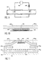
- a possible assembly is illustrated in FIG. 9, where we see a current generator 46 supplying the two halves of the detector in parallel and a winding 48 disposed anywhere in the circuit. As the bias current is continuous and the magnetic flux to be measured is at high frequency, the blocking inductor 48 will give at its terminals a voltage V proportional to the high frequency current.
- the detector of the invention has only two outputs instead of the conventional four, which significantly simplifies its mounting and connection.
- FIG. 10 shows a variant in which a thin magnetic layer 50, for example made of iron-nickel, of thickness between 30 and 200 nanometers, is placed under the detector 40. This layer channels the horizontal component of the field and increases the flux passing through the detector 40. This layer is thin enough to be saturated with writing.
- a thin magnetic layer 50 for example made of iron-nickel, of thickness between 30 and 200 nanometers
- FIG. 11 finally shows a complete magnetic head equipped according to the invention with a semiconductor field detector placed under the air gap.
- the numerical references are the same as in FIG. 1.
- the magnetic circuit is highly reluctant thanks to a separation between the concentrators 20 1 , 20 2 , and the pole pieces 22 1 , 22 2 .
Landscapes
- Engineering & Computer Science (AREA)
- Manufacturing & Machinery (AREA)
- Magnetic Heads (AREA)
- Measuring Magnetic Variables (AREA)
Applications Claiming Priority (2)
| Application Number | Priority Date | Filing Date | Title |
|---|---|---|---|
| FR9606083 | 1996-05-15 | ||
| FR9606083A FR2748843B1 (fr) | 1996-05-15 | 1996-05-15 | Tete magnetique a detecteur de champ a semiconducteur place sous l'entrefer |
Publications (1)
| Publication Number | Publication Date |
|---|---|
| EP0807925A1 true EP0807925A1 (de) | 1997-11-19 |
Family
ID=9492175
Family Applications (1)
| Application Number | Title | Priority Date | Filing Date |
|---|---|---|---|
| EP97400867A Withdrawn EP0807925A1 (de) | 1996-05-15 | 1997-04-21 | Magnetkopf mit unter der Spalte angeordnetem Halbleiterfelddetektor |
Country Status (3)
| Country | Link |
|---|---|
| EP (1) | EP0807925A1 (de) |
| JP (1) | JPH1074309A (de) |
| FR (1) | FR2748843B1 (de) |
Families Citing this family (1)
| Publication number | Priority date | Publication date | Assignee | Title |
|---|---|---|---|---|
| JP3604617B2 (ja) * | 2000-06-12 | 2004-12-22 | 富士通株式会社 | 磁気検出素子 |
Citations (9)
| Publication number | Priority date | Publication date | Assignee | Title |
|---|---|---|---|---|
| AU447091B1 (en) * | 1970-03-19 | 1972-06-08 | Amalgamated Wireless (Australasia) Limited | Magnetic field sensor |
| JPS55125688A (en) * | 1979-03-23 | 1980-09-27 | Toshiba Corp | Hall effect device |
| JPS57107087A (en) * | 1980-12-25 | 1982-07-03 | Toshiba Corp | Hall effect device |
| EP0406051A1 (de) * | 1989-06-27 | 1991-01-02 | Thomson-Csf | Hall-Effekt Magnetwiedergabekopf |
| JPH0393018A (ja) * | 1989-09-05 | 1991-04-18 | Hitachi Ltd | 磁気ヘッドおよびそれを用いた磁気記憶装置 |
| EP0443941A1 (de) * | 1990-02-21 | 1991-08-28 | Commissariat A L'energie Atomique | Horizontaler Magnetkopf mit Halleffekt und sein Herstellungsverfahren |
| JPH0644534A (ja) * | 1992-07-28 | 1994-02-18 | Tosoh Corp | 磁気ヘッド |
| FR2700633A1 (fr) * | 1993-01-20 | 1994-07-22 | Silmag Sa | Procédé de réalisation d'une tête magnétique à détecteur de champ à semiconducteur et tête obtenue par ce procédé. |
| JPH0817017A (ja) * | 1994-06-28 | 1996-01-19 | Japan Energy Corp | 薄膜積層型磁気ヘッド |
-
1996
- 1996-05-15 FR FR9606083A patent/FR2748843B1/fr not_active Expired - Fee Related
-
1997
- 1997-04-21 EP EP97400867A patent/EP0807925A1/de not_active Withdrawn
- 1997-05-14 JP JP9137986A patent/JPH1074309A/ja not_active Withdrawn
Patent Citations (10)
| Publication number | Priority date | Publication date | Assignee | Title |
|---|---|---|---|---|
| AU447091B1 (en) * | 1970-03-19 | 1972-06-08 | Amalgamated Wireless (Australasia) Limited | Magnetic field sensor |
| JPS55125688A (en) * | 1979-03-23 | 1980-09-27 | Toshiba Corp | Hall effect device |
| JPS57107087A (en) * | 1980-12-25 | 1982-07-03 | Toshiba Corp | Hall effect device |
| EP0406051A1 (de) * | 1989-06-27 | 1991-01-02 | Thomson-Csf | Hall-Effekt Magnetwiedergabekopf |
| JPH0393018A (ja) * | 1989-09-05 | 1991-04-18 | Hitachi Ltd | 磁気ヘッドおよびそれを用いた磁気記憶装置 |
| EP0443941A1 (de) * | 1990-02-21 | 1991-08-28 | Commissariat A L'energie Atomique | Horizontaler Magnetkopf mit Halleffekt und sein Herstellungsverfahren |
| JPH0644534A (ja) * | 1992-07-28 | 1994-02-18 | Tosoh Corp | 磁気ヘッド |
| FR2700633A1 (fr) * | 1993-01-20 | 1994-07-22 | Silmag Sa | Procédé de réalisation d'une tête magnétique à détecteur de champ à semiconducteur et tête obtenue par ce procédé. |
| EP0608173A1 (de) * | 1993-01-20 | 1994-07-27 | Silmag | Verfahren zur Herstellung eines Magnetkopfes mit Halbleiter-Feld-Detektor und auf diese Weise hergestellter Kopf |
| JPH0817017A (ja) * | 1994-06-28 | 1996-01-19 | Japan Energy Corp | 薄膜積層型磁気ヘッド |
Non-Patent Citations (6)
| Title |
|---|
| PATENT ABSTRACTS OF JAPAN vol. 004, no. 185 (E - 038) 19 December 1980 (1980-12-19) * |
| PATENT ABSTRACTS OF JAPAN vol. 006, no. 200 (E - 135) 9 October 1982 (1982-10-09) * |
| PATENT ABSTRACTS OF JAPAN vol. 015, no. 274 (P - 1226) 11 July 1991 (1991-07-11) * |
| PATENT ABSTRACTS OF JAPAN vol. 018, no. 278 (P - 1743) 26 May 1994 (1994-05-26) * |
| PATENT ABSTRACTS OF JAPAN vol. 96, no. 001 * |
| S.S. HEGEDUS: "Pezoresistive stress independant hall device", IBM TECHNICAL DISCLOSURE BULLETIN, vol. 22, no. 9, February 1980 (1980-02-01), ARMONK, N.Y., US, pages 4006 - 4008, XP002020670 * |
Also Published As
| Publication number | Publication date |
|---|---|
| FR2748843A1 (fr) | 1997-11-21 |
| FR2748843B1 (fr) | 1998-07-17 |
| JPH1074309A (ja) | 1998-03-17 |
Similar Documents
| Publication | Publication Date | Title |
|---|---|---|
| US7936631B2 (en) | Non-volatile memory element and method of operation therefor | |
| EP1435101B1 (de) | Magnetoresistive hochleistungs-spinventilanordnung | |
| KR100295289B1 (ko) | 후방자속가이드로서의감지층을갖는자기터널접합부자기저항판독헤드 | |
| US8072713B2 (en) | Magnetic reading head and magnetic recording apparatus | |
| US5084794A (en) | Shorted dual element magnetoresistive reproduce head exhibiting high density signal amplification | |
| JPH0697531A (ja) | 磁気抵抗効果素子 | |
| CN1215878A (zh) | 具体作为磁通引导的读出层的磁性隧道结磁阻读出磁头 | |
| EP0418372A1 (de) | Lese-magnetkopf mit magnetowiderstand für senkrechte aufzeichnung und herstellungsverfahren eines derartigen kopfes. | |
| FR2539542A1 (fr) | Tete magnetique de lecture | |
| EP0608173B1 (de) | Verfahren zur Herstellung eines Magnetkopfes mit Halbleiter-Feld-Detektor und auf diese Weise hergestellter Kopf | |
| EP0061363A1 (de) | Magnetoresistiver Lesewandler für grosse Informationsdichtheit | |
| EP0046697A1 (de) | Integrierter Magnetwandler | |
| WO1999022368A2 (en) | Magnetic field sensor comprising a spin-tunnel junction | |
| EP0781448B1 (de) | Planarer magnetkopf mit longitudinalem mehrschichtmagnetowiderstand | |
| US5914839A (en) | MR Device with anti-ferro magnetic field anti-parallel to sense current magnetic field | |
| JP2798122B2 (ja) | コルビーノ構造を用いた非磁性磁気抵抗効果型再生ヘッド | |
| EP0807925A1 (de) | Magnetkopf mit unter der Spalte angeordnetem Halbleiterfelddetektor | |
| EP0497069B1 (de) | Herstellungsverfahren von magnetoresistiven Sensoren und nach diesem Verfahren hergestellte magnetische Vorrichtung | |
| FR2648941A1 (fr) | Tete de lecture magnetique a effet hall | |
| EP1419506B1 (de) | Steuereinrichtung zur umkehr der magnetisierungsrichtung ohne ein externes magnetfeld | |
| FR2494952A1 (fr) | Transducteur magnetoresistant de lecture d'un support d'enregistrement a haute densite d'informations | |
| FR2496952A1 (fr) | Tete de transducteur magnetique a effet de magneto-resistance | |
| EP0779610B1 (de) | Aufzeichnungsvorrichtung mit Mikrospitze mit mehrschichtigem magnetoresistivem Überzug | |
| US5985471A (en) | Magnetic sensor | |
| KR100488638B1 (ko) | 자기저항소자를구비한단일채널자기헤드 |
Legal Events
| Date | Code | Title | Description |
|---|---|---|---|
| PUAI | Public reference made under article 153(3) epc to a published international application that has entered the european phase |
Free format text: ORIGINAL CODE: 0009012 |
|
| AK | Designated contracting states |
Kind code of ref document: A1 Designated state(s): DE GB IT |
|
| STAA | Information on the status of an ep patent application or granted ep patent |
Free format text: STATUS: THE APPLICATION IS DEEMED TO BE WITHDRAWN |
|
| 18D | Application deemed to be withdrawn |
Effective date: 19980520 |