EP0443941A1 - Horizontaler Magnetkopf mit Halleffekt und sein Herstellungsverfahren - Google Patents
Horizontaler Magnetkopf mit Halleffekt und sein Herstellungsverfahren Download PDFInfo
- Publication number
- EP0443941A1 EP0443941A1 EP91400440A EP91400440A EP0443941A1 EP 0443941 A1 EP0443941 A1 EP 0443941A1 EP 91400440 A EP91400440 A EP 91400440A EP 91400440 A EP91400440 A EP 91400440A EP 0443941 A1 EP0443941 A1 EP 0443941A1
- Authority
- EP
- European Patent Office
- Prior art keywords
- magnetic
- pole piece
- hall effect
- pillars
- insulating layer
- Prior art date
- Legal status (The legal status is an assumption and is not a legal conclusion. Google has not performed a legal analysis and makes no representation as to the accuracy of the status listed.)
- Withdrawn
Links
- 230000005355 Hall effect Effects 0.000 title claims abstract description 40
- 238000004519 manufacturing process Methods 0.000 title claims description 10
- 125000006850 spacer group Chemical group 0.000 claims abstract description 7
- 238000004804 winding Methods 0.000 claims description 19
- 239000000758 substrate Substances 0.000 claims description 13
- 238000000034 method Methods 0.000 claims description 10
- 239000000463 material Substances 0.000 claims description 7
- 239000004065 semiconductor Substances 0.000 claims description 6
- 238000005530 etching Methods 0.000 claims description 5
- 239000000696 magnetic material Substances 0.000 claims description 4
- 239000004020 conductor Substances 0.000 claims description 3
- VYPSYNLAJGMNEJ-UHFFFAOYSA-N Silicium dioxide Chemical compound O=[Si]=O VYPSYNLAJGMNEJ-UHFFFAOYSA-N 0.000 description 10
- 229910002555 FeNi Inorganic materials 0.000 description 5
- 229910052681 coesite Inorganic materials 0.000 description 5
- 229910052906 cristobalite Inorganic materials 0.000 description 5
- 239000000377 silicon dioxide Substances 0.000 description 5
- 235000012239 silicon dioxide Nutrition 0.000 description 5
- 229910052682 stishovite Inorganic materials 0.000 description 5
- 229910052905 tridymite Inorganic materials 0.000 description 5
- 238000005868 electrolysis reaction Methods 0.000 description 3
- 238000004544 sputter deposition Methods 0.000 description 3
- XUIMIQQOPSSXEZ-UHFFFAOYSA-N Silicon Chemical compound [Si] XUIMIQQOPSSXEZ-UHFFFAOYSA-N 0.000 description 2
- 238000000151 deposition Methods 0.000 description 2
- 230000008021 deposition Effects 0.000 description 2
- 230000004069 differentiation Effects 0.000 description 2
- 238000005259 measurement Methods 0.000 description 2
- 239000002184 metal Substances 0.000 description 2
- 238000001465 metallisation Methods 0.000 description 2
- 238000000206 photolithography Methods 0.000 description 2
- 229910052710 silicon Inorganic materials 0.000 description 2
- 239000010703 silicon Substances 0.000 description 2
- 230000000694 effects Effects 0.000 description 1
- 238000005516 engineering process Methods 0.000 description 1
- WPYVAWXEWQSOGY-UHFFFAOYSA-N indium antimonide Chemical compound [Sb]#[In] WPYVAWXEWQSOGY-UHFFFAOYSA-N 0.000 description 1
- 230000001939 inductive effect Effects 0.000 description 1
- 230000010287 polarization Effects 0.000 description 1
- 239000011347 resin Substances 0.000 description 1
- 229920005989 resin Polymers 0.000 description 1
- 230000035945 sensitivity Effects 0.000 description 1
- 239000010409 thin film Substances 0.000 description 1
Images


Classifications
-
- G—PHYSICS
- G11—INFORMATION STORAGE
- G11B—INFORMATION STORAGE BASED ON RELATIVE MOVEMENT BETWEEN RECORD CARRIER AND TRANSDUCER
- G11B5/00—Recording by magnetisation or demagnetisation of a record carrier; Reproducing by magnetic means; Record carriers therefor
- G11B5/127—Structure or manufacture of heads, e.g. inductive
- G11B5/33—Structure or manufacture of flux-sensitive heads, i.e. for reproduction only; Combination of such heads with means for recording or erasing only
- G11B5/37—Structure or manufacture of flux-sensitive heads, i.e. for reproduction only; Combination of such heads with means for recording or erasing only using galvano-magnetic devices, e.g. Hall-effect devices using Hall or Hall-related effect, e.g. planar-Hall effect or pseudo-Hall effect
- G11B5/376—Structure or manufacture of flux-sensitive heads, i.e. for reproduction only; Combination of such heads with means for recording or erasing only using galvano-magnetic devices, e.g. Hall-effect devices using Hall or Hall-related effect, e.g. planar-Hall effect or pseudo-Hall effect in semi-conductors
- G11B5/378—Integrated structures
Definitions
- the subject of the present invention is a horizontal Hall effect magnetic head and its production method. It applies in particular to the reading of a recording on a magnetic medium, but also to the writing on such a medium.
- FIG. 1 The structure of a horizontal writing and reading head for longitudinal recording is recalled in FIG. 1.
- a semiconductor substrate 10 are deposited and etched various layers (whose relative dimensions have not been respected for greater clarity) to form a magnetic circuit 12 with air gap filled by a non-magnetic spacer 14 and a conductive winding 16.
- This winding 16 comprises two series of windings connected together by a link 18; each of these series is wound around a magnetic pillar 20, 21.
- These magnetic pillars 20, 21 connect the first and second horizontal pole pieces 22, 23 of the circuit 12.
- the coil 16 is connected at its two ends, by means of links 24, 26 passing through the substrate 10, to contact pads 28, 30 arranged on the underside of the substrate.
- the write and / or read track 32 scrolls above the air gap.
- Document FR 2 518 792 discloses a vertical magnetic head using a Hall effect sensor.
- a magnetic head is shown schematically in Figure 2.
- the Hall effect sensor 34 is arranged in a space between two pole pieces 36, 38. These pole pieces 36, 38 are placed vertically relative to the magnetic recording medium 32 and are separated at the level of the part of the head close to the medium by a non-magnetic spacer 40.
- Such a magnetic head only has a single Hall effect sensor; it therefore undergoes thermal or electronic drifts which must be compensated for elsewhere.
- FIG. 3 schematically represents another known vertical magnetic head and comprising a Hall effect sensor. This magnetic head is described in detail in document US 3,800,193.
- the pole pieces 36, 38 meet at each of their ends. They are separated on the one hand by a non-magnetic spacer 40 at the level of the part of the pole pieces facing the magnetic recording medium 32 and on the other hand by the Hall effect sensor 34.
- This magnetic head has the same drawbacks as the previous one.
- the object of the present invention is to provide a horizontal magnetic head which comprises at least one Hall effect sensor and which offers the possibility of overcoming these problems of drift by a simple differential measurement.
- the present invention relates to a horizontal magnetic head with effect Hall comprising, contained in a box formed in a semiconductor substrate, a first horizontal pole piece, a second horizontal pole piece in two parts separated by a non-magnetic spacer, a first magnetic pillar connecting the first pole piece to a part of the second pole piece , a second magnetic pillar connecting the first pole piece to the other part of the second pole piece, characterized in that at least one of the pillars comprises a Hall effect sensor.
- the position of the sensors in the height of the pillars is irrelevant for the functioning of the head.
- the magnetic head of the invention is horizontal: it has two magnetic pillars which can each integrate a Hall effect sensor.
- the presence of two sensors makes it possible to simply carry out a differential measurement of the signals for reading a recorded magnetic medium delivered by each of the sensors and to obtain a signal free of any drift.
- this signal is of twice the intensity of the signal delivered by a single sensor.
- each pillar comprises a Hall effect sensor
- these sensors are connected by outputs to the inputs of a differential circuit delivering a read signal on an output.
- the invention provides an additional advantage: it is possible to integrate on a single head both reading means (of which the Hall effect sensor or sensors are part) and writing means, these reading means and writing using the same magnetic circuit.
- the magnetic head according to the invention further comprises a conductive winding surrounding the two magnetic pillars.
- a conductive winding is also formed surrounding the two magnetic pillars during the step of producing the conductive pads.
- the conductive pads and the ends of the winding are connected by metal links to the outside of the substrate. These metal connections are obtained in a conventional manner either by etching the rear face of the substrate and the first insulating layer and metallization of the etched holes for example before the step of forming the conductive pads, or by etching the front face of the sixth, fifth and fourth insulating layers and metallization of the etched holes, at the end of the manufacturing process.
- FIG 4 there is shown a sectional view of a semiconductor substrate 10, for example of silicon, in which has been etched a box.
- a horizontal magnetic layer 42 for example made of FeNi, forms a first pole piece of the magnetic circuit, is grown at the bottom of this box, by electrolysis.
- the first pole piece 42 is covered with an insulating layer 44, for example made of SiO2.
- FIG. 5 represents a section of the head.
- first insulating layer 44 On the first insulating layer 44 are deposited, in the vicinity and preferably around each end of the first pole piece 42, four conductive pads (only the pads 46, 48 and 54, 56 are shown in the section) surrounded by the windings of a conductive winding. This winding is formed by two series of windings 62a and 62b connected together.
- the assembly is covered with a second insulating layer 64, for example made of SiO2, which is selectively etched in a conventional manner to form two openings, facing the ends of the first pole piece. These openings are filled, by electrolytic deposition for example, to form two magnetic half-pillars 66, 68, for example made of FeNi, flush with the surface of the second insulating layer 64.
- a second insulating layer 64 for example made of SiO2
- These openings are filled, by electrolytic deposition for example, to form two magnetic half-pillars 66, 68, for example made of FeNi, flush with the surface of the second insulating layer 64.
- the assembly is covered by an insulating layer 70, for example made of SiO2, of thickness X preferably small, for example 0.2 micrometer.
- FIG. 6 represents a partial top view of the device after carrying out the operations described above. It can be seen in this figure that the half-pillar 66 is surrounded by the conductive pads 46, 48, 50, 52 and that the half-pillar 68 is surrounded by the conductive pads 54, 56, 58, 60.
- the pads 48 and 54 inside the magnetic circuit have an elongated strip shape so as to allow contact to be made without having to pass through the first pole piece 42 as will be seen more precisely below.
- Each series 62a and 62b of the winding comprises ten windings for example.
- FIG. 7 shows the result of the following steps of the production method on a sectional view.
- openings are made in the insulating layers 64 and 70. These openings reach the conductive pads 46, 48, 50, 52, 54, 56, 58, 60.
- a layer 72 of Hall effect material for example InSb, of thickness Y equal, for example, to 1 micrometer. This deposition is carried out for example by sputtering.
- the shape of the sensors is defined by photolithography and etching.
- Figure 7 there is shown the resin mask 74, 76 for defining the shape of the sensors during etching.
- FIG. 8 schematically represents the result of the following steps of the production method.
- the sensors 78 and 80 are engraved so as to be integrated into the magnetic pillars. They are connected to the conductive pads on either side of the half-pillars 66, 68.
- a fourth insulating layer 82 for example made of SiO2, of thickness Z equal for example to 0.2 micrometer perpendicular to the sensors, is deposited on the assembly.
- FIG. 9 schematically represents a top view of a Hall effect sensor integrated in a magnetic pillar.
- the sensor 78 shown has dimensions substantially greater than the section of the half-pillar 66.
- the sensor 78 is furthermore provided with protruding tabs 84, 86, 88, 90 for contacts with the conductive pads 46, 52, 48 and 50, respectively.
- FIG. 10 schematically illustrates the result of the following steps of the method.
- the upper half-pillars 92 and 94 are produced directly above the half-pillars 66 and 68 respectively.
- the half-pillars are for example made of FeNi.
- These half-pillars 92 and 94 are made in openings made in a fifth insulating layer 96, for example in SiO2 previously deposited on the assembly, either by sputtering, for example FeNi in this fifth layer and surfacing, or by electrolysis.
- a conductive material is deposited beforehand on the fifth insulating layer provided with these openings, for example by sputtering, then an electrolysis of the magnetic material chosen is carried out using the conductive material as an electrode and finally a surfacing of the assembly in order to form the pillars.
- the total height L of the pillars is for example 10 micrometers.
- FIG. 11 shows diagrammatically in section, a magnetic head according to the invention at the end of the production process.
- An upper pole piece for example made of FeNi in two parts 98, 100 separated by a non-magnetic spacer 102 is produced for example according to the technique described in document EP-A-0 262 028 (FIGS. 5j, 5k, 5l, 5m).
- the substrate 10 and the first insulating layer 44 are pierced with openings (only two referenced 104 and 106 are visible in the sectional view) allowing access to the conductive pads from the rear of the head magnetic.
- openings allow the sensors 78, 80 to be connected in a conventional manner on the one hand to processing means such as a differential circuit and on the other hand to an electrical supply circuit.
- openings 105a and 105b are drilled to allow the connections between the winding and supply means (not shown).
- An example of how these connections are made is described in the document "Electrical connection through silicon wafer” published in the Journal of Electrochemical Society - Fall Meeting, Chicago, October 9 to 14, 1988.
- Hall effect sensors are only used for reading a magnetic signal recorded on a traveling medium parallel to the second horizontal pole piece.
- the sensors 78 and 80 are supplied with current by current generators 108, 110 respectively connected to the pads 50 and 58.
- the pads 52 and 60 are grounded.
- the Hall voltage due to the crossing of the sensors by the lines of the magnetic field B is measured between the pads 46, 48 for the sensor 78 and 54, 56 for the sensor 80. These voltages each include a Hall component due to the crossing of the sensors by magnetic field lines.
- the voltages also include a noise component which is added to the Hall component of one of the sensors and which is subtracted from the Hall component of the other of the sensors.
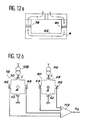
- the Hall voltage delivered by the sensor 80 is applied to the inputs (+) of a differential circuit 112.
- the Hall voltage delivered by the sensor 78 is applied to the inputs (-) of this circuit 112.
- the latter delivers a signal exit VS not only having a double amplitude of the signals delivered by each sensor but also free of any noise and in particular of any thermal drift or other eliminated during differentiation. These Hall components are equal but with opposite signs.
- This last figure represents a gain of around 20 compared to inductive heads using a read winding.
- the invention uses a winding, preferably with a small number of turns (for example 10) to obtain a reduced magnetic circuit in order to compensate for the losses in efficiency of the head at the writing due to the secondary air gaps made in the pillars to incorporate the Hall effect sensors.
- the magnetic Hall effect head can be used for reading but also for writing thanks to the winding 62a, 62b. To obtain a read head only, it suffices to omit this winding during the production process.
- the deposits of the various magnetic materials are here of the electrolytic type but any other type of deposit can be used.
- the device presented comprises two Hall effect sensors (one in each pillar), but a device comprising only one Hall effect sensor integrated in one of the two pillars belongs to the scope of the present invention.
Landscapes
- Engineering & Computer Science (AREA)
- Manufacturing & Machinery (AREA)
- Magnetic Heads (AREA)
- Hall/Mr Elements (AREA)
- Measuring Magnetic Variables (AREA)
Applications Claiming Priority (2)
| Application Number | Priority Date | Filing Date | Title |
|---|---|---|---|
| FR9002113 | 1990-02-21 | ||
| FR9002113A FR2658647B1 (fr) | 1990-02-21 | 1990-02-21 | Tete magnetique horizontale a effet hall et son procede de realisation. |
Publications (1)
| Publication Number | Publication Date |
|---|---|
| EP0443941A1 true EP0443941A1 (de) | 1991-08-28 |
Family
ID=9393970
Family Applications (1)
| Application Number | Title | Priority Date | Filing Date |
|---|---|---|---|
| EP91400440A Withdrawn EP0443941A1 (de) | 1990-02-21 | 1991-02-19 | Horizontaler Magnetkopf mit Halleffekt und sein Herstellungsverfahren |
Country Status (4)
| Country | Link |
|---|---|
| US (1) | US5166849A (de) |
| EP (1) | EP0443941A1 (de) |
| JP (1) | JPH04251418A (de) |
| FR (1) | FR2658647B1 (de) |
Cited By (5)
| Publication number | Priority date | Publication date | Assignee | Title |
|---|---|---|---|---|
| FR2700633A1 (fr) * | 1993-01-20 | 1994-07-22 | Silmag Sa | Procédé de réalisation d'une tête magnétique à détecteur de champ à semiconducteur et tête obtenue par ce procédé. |
| EP0801379A1 (de) * | 1996-04-12 | 1997-10-15 | Silmag | Herstellungsverfahren eines Magnetkopfes mit Halbleiter-Felddetektor und nach diesem Verfahren hergestellter Kopf |
| FR2747497A1 (fr) * | 1996-04-12 | 1997-10-17 | Silmag Sa | Tete magnetique a detecteur de champ optimise |
| EP0807925A1 (de) * | 1996-05-15 | 1997-11-19 | Silmag | Magnetkopf mit unter der Spalte angeordnetem Halbleiterfelddetektor |
| EP0811966A1 (de) * | 1996-06-06 | 1997-12-10 | Silmag | Magnetaufzeichnungs- und -wiedergabekopf mit Halbleiter-Feldsensor |
Families Citing this family (11)
| Publication number | Priority date | Publication date | Assignee | Title |
|---|---|---|---|---|
| US5251082A (en) * | 1991-06-13 | 1993-10-05 | Elliott Timothy J | Miniaturized disk file pluggable into a card terminal |
| US5378885A (en) * | 1991-10-29 | 1995-01-03 | Mars Incorporated | Unshielded magnetoresistive head with multiple pairs of sensing elements |
| US5358088A (en) * | 1992-11-25 | 1994-10-25 | Mars Incorporated | Horizontal magnetoresistive head apparatus and method for detecting magnetic data |
| US5543988A (en) * | 1993-04-30 | 1996-08-06 | International Business Machines Corporation | Hall sensor with high spatial resolution in two directions concurrently |
| FR2709855B1 (fr) * | 1993-09-06 | 1995-10-20 | Commissariat Energie Atomique | Tête magnétique de lecture et d'écriture à élément magnétorésistant compensé en écriture. |
| US5475590A (en) * | 1993-10-22 | 1995-12-12 | Ford Motor Company | Automatic transmission torque converter bypass clutch control using engine torque compensation |
| US6195228B1 (en) | 1997-01-06 | 2001-02-27 | Nec Research Institute, Inc. | Thin, horizontal-plane hall sensors for read-heads in magnetic recording |
| IL141859A0 (en) * | 1998-09-24 | 2002-03-10 | Materials Innovation Inc | Magnetoresistive device, giant magnetoresistive device and methods for making same |
| JP3955195B2 (ja) * | 2001-08-24 | 2007-08-08 | 株式会社日立グローバルストレージテクノロジーズ | 磁界センサー及び磁気ヘッド |
| EP2382661B1 (de) | 2008-12-30 | 2021-08-11 | STMicroelectronics Srl | Integrierte elektronische einrichtung mit sende-/empfangsantenne und magnetischer verbindung |
| US8107197B2 (en) | 2008-12-30 | 2012-01-31 | Hitachi Global Storage Technologies Netherlands B.V. | Slider with integrated writer and semiconductor heterostucture read sensor |
Citations (5)
| Publication number | Priority date | Publication date | Assignee | Title |
|---|---|---|---|---|
| GB970455A (en) * | 1962-02-02 | 1964-09-23 | Philips Electronic Associated | Improvements in or relating to magnetic playback heads |
| US3355727A (en) * | 1963-07-24 | 1967-11-28 | Donald C Gaubatz | Shield utilized as flux path for magnetic head |
| US3800193A (en) * | 1972-09-05 | 1974-03-26 | Ibm | Magnetic sensing device |
| EP0269129A2 (de) * | 1986-11-28 | 1988-06-01 | Nec Corporation | Dünnfilmmagnetkopf |
| EP0284495A2 (de) * | 1987-03-19 | 1988-09-28 | Commissariat A L'energie Atomique | Magnetkopf zum Lesen von Spuren mit sehr schmaler Breite und Herstellungverfahren |
Family Cites Families (1)
| Publication number | Priority date | Publication date | Assignee | Title |
|---|---|---|---|---|
| FR2461995A1 (fr) * | 1979-07-20 | 1981-02-06 | Lcc Cice Cie Europ Compo Elect | Transducteur magneto-electrique pour systeme d'enregistrement magnetique, et systeme d'enregistrement comportant un tel transducteur |
-
1990
- 1990-02-21 FR FR9002113A patent/FR2658647B1/fr not_active Expired - Lifetime
-
1991
- 1991-02-08 US US07/652,994 patent/US5166849A/en not_active Expired - Fee Related
- 1991-02-19 EP EP91400440A patent/EP0443941A1/de not_active Withdrawn
- 1991-02-21 JP JP3049248A patent/JPH04251418A/ja not_active Withdrawn
Patent Citations (5)
| Publication number | Priority date | Publication date | Assignee | Title |
|---|---|---|---|---|
| GB970455A (en) * | 1962-02-02 | 1964-09-23 | Philips Electronic Associated | Improvements in or relating to magnetic playback heads |
| US3355727A (en) * | 1963-07-24 | 1967-11-28 | Donald C Gaubatz | Shield utilized as flux path for magnetic head |
| US3800193A (en) * | 1972-09-05 | 1974-03-26 | Ibm | Magnetic sensing device |
| EP0269129A2 (de) * | 1986-11-28 | 1988-06-01 | Nec Corporation | Dünnfilmmagnetkopf |
| EP0284495A2 (de) * | 1987-03-19 | 1988-09-28 | Commissariat A L'energie Atomique | Magnetkopf zum Lesen von Spuren mit sehr schmaler Breite und Herstellungverfahren |
Non-Patent Citations (1)
| Title |
|---|
| IBM TECHNICAL DISCLOSURE BULLETIN. vol. 12, no. 12, mai 1970, ARMONK,N.Y.,USA page 2163 _T:W. COLLINS et al.: "ELIMINATION OF DC OFFSET POTENTIAL OF HALL EFFECT DEVICES" * |
Cited By (10)
| Publication number | Priority date | Publication date | Assignee | Title |
|---|---|---|---|---|
| FR2700633A1 (fr) * | 1993-01-20 | 1994-07-22 | Silmag Sa | Procédé de réalisation d'une tête magnétique à détecteur de champ à semiconducteur et tête obtenue par ce procédé. |
| EP0608173A1 (de) * | 1993-01-20 | 1994-07-27 | Silmag | Verfahren zur Herstellung eines Magnetkopfes mit Halbleiter-Feld-Detektor und auf diese Weise hergestellter Kopf |
| US5476804A (en) * | 1993-01-20 | 1995-12-19 | Silmag | Process for producing a semiconductor field detector magnetic head |
| EP0801379A1 (de) * | 1996-04-12 | 1997-10-15 | Silmag | Herstellungsverfahren eines Magnetkopfes mit Halbleiter-Felddetektor und nach diesem Verfahren hergestellter Kopf |
| FR2747498A1 (fr) * | 1996-04-12 | 1997-10-17 | Silmag Sa | Procede de realisation d'une tete magnetique a detecteur de champ a semiconducteur et tete obtenue par ce procede |
| FR2747497A1 (fr) * | 1996-04-12 | 1997-10-17 | Silmag Sa | Tete magnetique a detecteur de champ optimise |
| EP0807925A1 (de) * | 1996-05-15 | 1997-11-19 | Silmag | Magnetkopf mit unter der Spalte angeordnetem Halbleiterfelddetektor |
| FR2748843A1 (fr) * | 1996-05-15 | 1997-11-21 | Silmag Sa | Tete magnetique a detecteur de champ a semiconducteur place sous l'entrefer |
| EP0811966A1 (de) * | 1996-06-06 | 1997-12-10 | Silmag | Magnetaufzeichnungs- und -wiedergabekopf mit Halbleiter-Feldsensor |
| FR2749695A1 (fr) * | 1996-06-06 | 1997-12-12 | Silmag Sa | Tete magnetique d'ecriture et de lecture a detecteur de champ a semiconducteur |
Also Published As
| Publication number | Publication date |
|---|---|
| FR2658647B1 (fr) | 1992-04-30 |
| JPH04251418A (ja) | 1992-09-07 |
| FR2658647A1 (fr) | 1991-08-23 |
| US5166849A (en) | 1992-11-24 |
Similar Documents
| Publication | Publication Date | Title |
|---|---|---|
| FR2658647A1 (fr) | Tete magnetique horizontale a effet hall et son procede de realisation. | |
| EP0284495B1 (de) | Magnetkopf zum Lesen von Spuren mit sehr schmaler Breite und Herstellungverfahren | |
| EP0420755B1 (de) | Herstellungsverfahren eines Magnetaufzeichnungskopfes und nach diesem Verfahren erhaltener Kopf | |
| WO1990011594A1 (fr) | Tete magnetique de lecture a magnetoresistance pour enregistrement perpendiculaire et procede de realisation d'une telle tete | |
| FR2604021A1 (fr) | Procede de realisation de tetes magnetiques en couches minces et a structure planaire et tete obtenue par ce procede | |
| EP0467736B1 (de) | Magnetoresistiver Effekt verwendender Lesemagnetkopf | |
| FR2954854A1 (fr) | Photodetecteur a structure plasmon | |
| EP0046697B1 (de) | Integrierter Magnetwandler | |
| EP0642030B1 (de) | Flussleiter mit Zungen und magnetischer Sensor mit einem solchen Flussleiter | |
| EP0608173A1 (de) | Verfahren zur Herstellung eines Magnetkopfes mit Halbleiter-Feld-Detektor und auf diese Weise hergestellter Kopf | |
| EP0642181B1 (de) | Magnetoresistive Anordnung und Fühler mit wiederholenden geometrischen Strukturen | |
| EP0702358A1 (de) | Magnetkopf mit unterliegendem longitudinalem Mehrschicht-Magnetowiderstand | |
| WO2000036429A1 (fr) | Capteur de champ magnetique a magnetoresistance geante | |
| EP0781448B1 (de) | Planarer magnetkopf mit longitudinalem mehrschichtmagnetowiderstand | |
| EP0040994B1 (de) | Magnetwandler, der einen Spalt mit veränderbarer Grössen-Dimension aufweist, zur Wiedergabe oder zum Aufzeichnen von Informationen eines magnetischen Trägers | |
| EP0406051A1 (de) | Hall-Effekt Magnetwiedergabekopf | |
| EP0497069B1 (de) | Herstellungsverfahren von magnetoresistiven Sensoren und nach diesem Verfahren hergestellte magnetische Vorrichtung | |
| FR2575314A1 (fr) | Transducteur magnetique d'ecriture pour enregistrement transversal | |
| EP0269489B1 (de) | Herstellungsverfahren eines Magnetkopfes zur Vereinfachung der Herstellung von elektrischen Anschlüssen | |
| FR2802011A1 (fr) | Tete de lecture planaire a element magneto-resistif | |
| FR2761477A1 (fr) | Capteur de champ magnetique a magnetoresistance | |
| EP0658772A1 (de) | Magnetischer Fühler mit magnetoresistivem Effekt | |
| EP3646046B1 (de) | Vorrichtung zur messung schwacher magnetfelder | |
| FR2806826A1 (fr) | Tete magnetique integree pour l'enregistrement magnetique helicoidal sur bande et son procede de fabrication | |
| FR2880473A1 (fr) | Memoire vive magnetique |
Legal Events
| Date | Code | Title | Description |
|---|---|---|---|
| PUAI | Public reference made under article 153(3) epc to a published international application that has entered the european phase |
Free format text: ORIGINAL CODE: 0009012 |
|
| AK | Designated contracting states |
Kind code of ref document: A1 Designated state(s): BE CH DE GB IT LI NL |
|
| 17P | Request for examination filed |
Effective date: 19920205 |
|
| STAA | Information on the status of an ep patent application or granted ep patent |
Free format text: STATUS: THE APPLICATION IS DEEMED TO BE WITHDRAWN |
|
| 18D | Application deemed to be withdrawn |
Effective date: 19940830 |