EP0808060B1 - Circuit amplificateur avec filtre pour signaux numériques et analogiques - Google Patents
Circuit amplificateur avec filtre pour signaux numériques et analogiques Download PDFInfo
- Publication number
- EP0808060B1 EP0808060B1 EP97107281A EP97107281A EP0808060B1 EP 0808060 B1 EP0808060 B1 EP 0808060B1 EP 97107281 A EP97107281 A EP 97107281A EP 97107281 A EP97107281 A EP 97107281A EP 0808060 B1 EP0808060 B1 EP 0808060B1
- Authority
- EP
- European Patent Office
- Prior art keywords
- filter
- amplifier circuit
- digital
- signal
- analog
- Prior art date
- Legal status (The legal status is an assumption and is not a legal conclusion. Google has not performed a legal analysis and makes no representation as to the accuracy of the status listed.)
- Expired - Lifetime
Links
- 238000010897 surface acoustic wave method Methods 0.000 claims description 5
- 238000011161 development Methods 0.000 description 4
- 230000018109 developmental process Effects 0.000 description 4
- 238000010586 diagram Methods 0.000 description 3
- 108010076504 Protein Sorting Signals Proteins 0.000 description 1
- 230000009286 beneficial effect Effects 0.000 description 1
- 239000000969 carrier Substances 0.000 description 1
- 230000001934 delay Effects 0.000 description 1
- 230000001419 dependent effect Effects 0.000 description 1
- 238000000034 method Methods 0.000 description 1
- 238000003672 processing method Methods 0.000 description 1
- 230000001629 suppression Effects 0.000 description 1
Images


Classifications
-
- H—ELECTRICITY
- H04—ELECTRIC COMMUNICATION TECHNIQUE
- H04N—PICTORIAL COMMUNICATION, e.g. TELEVISION
- H04N5/00—Details of television systems
- H04N5/44—Receiver circuitry for the reception of television signals according to analogue transmission standards
- H04N5/4446—IF amplifier circuits specially adapted for B&W TV
-
- H—ELECTRICITY
- H04—ELECTRIC COMMUNICATION TECHNIQUE
- H04N—PICTORIAL COMMUNICATION, e.g. TELEVISION
- H04N21/00—Selective content distribution, e.g. interactive television or video on demand [VOD]
- H04N21/40—Client devices specifically adapted for the reception of or interaction with content, e.g. set-top-box [STB]; Operations thereof
- H04N21/41—Structure of client; Structure of client peripherals
- H04N21/426—Internal components of the client ; Characteristics thereof
-
- H—ELECTRICITY
- H04—ELECTRIC COMMUNICATION TECHNIQUE
- H04N—PICTORIAL COMMUNICATION, e.g. TELEVISION
- H04N5/00—Details of television systems
- H04N5/44—Receiver circuitry for the reception of television signals according to analogue transmission standards
- H04N5/46—Receiver circuitry for the reception of television signals according to analogue transmission standards for receiving on more than one standard at will
Definitions
- the invention is based on an amplifier circuit Filters for digital and analog signals according to the generic term of claim 1.
- the IF amplifier must be used for each standard select appropriate signals. The selection takes place in the ZF area on a fixed frequency.
- Filters are used for selection. With analog reception, a Nyquist edge needed to get a suitable signal. This is not necessary for a digital signal.
- EP-A 0 006 510 is an IF amplifier for multi-standard television receivers known.
- the known amplifier for all standards use the same surface acoustic wave filter.
- DE-A 44 27 396 describes a processing method known from digital and analog input signals. With this Procedures become dependent on whether digital or analog signals be received, a vibration generator different Components switched on.
- the invention has for its object with little Effort to create a circuit that is both analog as well digital signals processed. This task is accomplished by a Amplifier circuit according to claim 1 solved. Beneficial Further developments of the invention are in the subclaims specified.
- filters for digital and analog Signals used.
- the filters for digital signal reception are connected to the analog filters for analog signal reception.
- By connecting the digital filter in front of the analog one It is possible to filter in addition to Main selection required selection means for the analog signal to renounce.
- the analog Filter With digital signal reception, the analog Filter not activated because the digital signal requires the largest possible bandwidth, but the analog filter needs the would limit bandwidth.
- the filters for analog and digital Signal processing becomes a decoupling stage used.
- the decoupling stage is preferably as Emitter follower trained.
- the filters for analog and digital Signal processing is formed from surface wave filters.
- the filters are preferably arranged in cascade.
- the Surface wave filters amplitude frequency response and Group runtime characteristics designed independently of each other can be. By cascading a desired one Group delay for the analog signal output more flexible be designed. This is possible by overlaying the Group runtimes of the analog and digital Surface wave filter. Otherwise inevitable ripples in the Signal curve at the output of the analog surface wave filter can by the cascade connection and its antiphase Signal curve from the digital surface wave filter HS2 be compensated.
- the desired group runtime of the analog surface wave filter can be matched by the appropriate Course of the digital surface wave filter can be achieved.
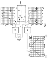
- Fig. 1 shows a known amplifier circuit.
- the IF signal from the tuner which is not shown here, passes through point A in analog path 1 and in digital path 2.
- Analog path 1 is formed from selection means ZS and the Surface wave filter HS1.
- the digital path is formed through the surface wave filter HS2.
- the switch S the Signal processing stage IC switches the signal for the analog Reception or digital reception for further processing in the Signal processing stage IC through.
- At point B is the signal shown, which is characterized by the surface wave filter HS2 results.
- the signal is shown, which is characterized by the additional selection means ZS and the Surface wave filter HS1 results.
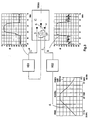
- the IF signal of the tuner passes from point A via the Surface wave filter HS2 at point B. Arrived from point B. the signal to input 4 of switch S in the IC signal processing stage. The signal comes from point B. continue via the emitter follower EF to the Surface wave filter HS1. From the surface wave filter HS1 the signal arrives at input 3 of the via point C * Switch S.
- the switch S switches depending on the type of received signal to input 3 for analog signals or input 4 for digital signals. Switching the Switch S is done by the signal processing stage IC. The Distinguish whether a digital or analog signal is received is determined, the signal processing stage IC from the Signal sequence.
- the user can program the received transmitter of the signal processing stage IC notifies whether it is an analog or digital receive signal.
- the Signal processing level that selected under this Program position an analog or digital signal is received, and the switch is accordingly in switch position 3 or 4 switched.
- the deleted selection means ZS were used for Suppression of unwanted signals like neighboring carriers.
- the Surface wave filter HS2 has a pass band that is larger than that of the surface acoustic wave filter HS1. This will make the Passband of filter HS1 not affected. Outside the passband is an additional selection reached.
- the selection means ZS are therefore no longer necessary, since the two surface wave filters are cascaded HS2 and HS1 an overall selection is achieved for the analog signal processing can be used.
- FIG. 3 shows a further development of the invention Solution.
- the emitter follower EF is in the signal processing stage IC has been integrated.
- the circuit works otherwise as below Fig. 2 described.
- HS2 amplitude frequency response and group delay characteristics can be designed independently.
- Cascading can create a desired group delay at the point C * (Fig. 2, 3) by superimposing the group delays in the surface wave filters HS1, HS2 can be made more flexible. Otherwise unavoidable ripples in the output signal of the Surface wave filter HS1 (Fig. 1, point C) can by Cascade connection due to its phase opposition from the Surface wave filter HS2 can be compensated (Fig. 2.3 point C *).
- the desired group runtime in the Surface wave filter HS1 can by the adapted course of the surface wave filter HS2 can be obtained.
- FIG. 4 shows a further development of the invention Circuit.
- the modules are summarized in the circuit diagram and been marked as blocks in the previous figures are shown. How it works and how it works Components have been explained using the block diagrams. It it can be clearly seen that there is only one signal input A.
- the surface wave filter HS2 is located after this signal input A. for the digital signal path.
- the signal then arrives at Emitter follower EF and via pins 4 and 5 in the integrated IC circuit.
- the measuring point B was in the block diagrams the emitter follower and also the signal was before the emitter follower tapped. In this built-up circuit, the signal tapped behind the emitter follower, so this filter too can still be used for the digital part.
- the Signal curve at point B is identical to the signal curve of the previous point B from Fig. 2 and 3.
- the signal goes to the analog surface wave filter HS1.
- the analog part is divided into picture and sound and marked through the outputs C1 "analog vision" and C2 "analog sound".
- Advantageous and different from FIGS. 2 and 3 is that the Emitter follower EF for both the digital and the analog part is used.
Landscapes
- Engineering & Computer Science (AREA)
- Multimedia (AREA)
- Signal Processing (AREA)
- Superheterodyne Receivers (AREA)
- Amplifiers (AREA)
- Noise Elimination (AREA)
- Analogue/Digital Conversion (AREA)
Claims (7)
- Circuit amplificateur pour des signaux à fréquence intermédiaire de différentes normes pour le traitement au choix de signaux numériques et analogiques,caratérisé en ce que la sortie du premier filtre (HS2) est reliée à l'entrée du deuxième filtre (HS1),avec une entrée (A) pour la réception au choix de signaux numériques et analogiques,avec un premier chemin (2), qui présente un premier filtre (HS2), pour le traitement de signaux numériques,avec un deuxième chemin (1), qui présente un deuxième filtre (HS1), pour le traitement de signaux analogiques,en ce qu'un dispositif de commutation (S) est prévu, sa première entrée (4) étant reliée à la sortie du premier filtre (HS2), sa deuxième entrée (3) étant reliée à la sortie du premier filtre (HS1) et sa sortie fournit un signal pour le traitement ultérieur, eten ce que le dispositif de commutation (S) est commandé de sorte que, lors de la réception de signaux numériques, la deuxième sortie (3) du dispositif de commutation (S) est reliée à sa sortie.
- Circuit amplificateur conforme à la revendication 1, caractérisé en ce que les filtres (HS1, HS2) sont constitués comme des filtres d'ondes de surface.
- Circuit amplificateur conforme à la revendication 1, caractérisé en ce que les filtres (HS1, HS2) sont montés en cascade.
- Circuit amplificateur conforme à la revendication 1, caractérisé en ce que les filtres (HS1, HS2) sont reliés entre eux via un étage de découplage (EF).
- Circuit amplificateur conforme à la revendication 4, caractérisé en ce que l'étage de découplage (EF) est constitué comme un émetteur-suiveur.
- Circuit amplificateur conforme à la revendication 1, caractérisé en ce que la totalité de la courbe du temps de propagation de groupe est modifiable par le temps de propagation de groupe des filtres d'ondes de surface (HS1, HS2).
- Circuit amplificateur conforme à la revendication 1, caractérisé en ce que la totalité de la courbe de réponse en fréquences d'amplitude est modifiable par la réponse en fréquences d'amplitude des filtres d'ondes de surface (HS1, HS2).
Applications Claiming Priority (2)
| Application Number | Priority Date | Filing Date | Title |
|---|---|---|---|
| DE19619750 | 1996-05-15 | ||
| DE19619750A DE19619750A1 (de) | 1996-05-15 | 1996-05-15 | Verstärkerschaltung mit Filter für digitale und analoge Signale |
Publications (3)
| Publication Number | Publication Date |
|---|---|
| EP0808060A2 EP0808060A2 (fr) | 1997-11-19 |
| EP0808060A3 EP0808060A3 (fr) | 1999-02-24 |
| EP0808060B1 true EP0808060B1 (fr) | 2001-12-12 |
Family
ID=7794476
Family Applications (1)
| Application Number | Title | Priority Date | Filing Date |
|---|---|---|---|
| EP97107281A Expired - Lifetime EP0808060B1 (fr) | 1996-05-15 | 1997-05-02 | Circuit amplificateur avec filtre pour signaux numériques et analogiques |
Country Status (4)
| Country | Link |
|---|---|
| EP (1) | EP0808060B1 (fr) |
| JP (1) | JP4050354B2 (fr) |
| CN (1) | CN1083639C (fr) |
| DE (2) | DE19619750A1 (fr) |
Families Citing this family (5)
| Publication number | Priority date | Publication date | Assignee | Title |
|---|---|---|---|---|
| AU4477500A (en) * | 1999-04-20 | 2000-11-02 | Thomson Licensing S.A. | If signal processing apparatus |
| US7202910B1 (en) | 1999-04-20 | 2007-04-10 | Thomson Licensing | Signal processing apparatus |
| DE10163798A1 (de) * | 2001-12-22 | 2003-07-03 | Philips Intellectual Property | Fernsehsignal-Empfänger mit universalem Ausgang für verschiedenartige Oberflächenwellenfilter |
| CN104618666B (zh) | 2013-11-05 | 2018-04-10 | 南宁富桂精密工业有限公司 | 音频信号控制电路 |
| CN105978533A (zh) * | 2016-06-18 | 2016-09-28 | 南通尚青医疗科技有限公司 | 一种复合滤波器 |
Family Cites Families (8)
| Publication number | Priority date | Publication date | Assignee | Title |
|---|---|---|---|---|
| DE3120050A1 (de) * | 1981-05-20 | 1982-12-09 | Licentia Patent-Verwaltungs-Gmbh, 6000 Frankfurt | Zf-verstaerker fuer einen mehrnormen-fernsehempfaenger |
| US4868516A (en) * | 1988-04-14 | 1989-09-19 | John Fluke Mfg. Co., Inc. | Alternating current amplifier with digitally controlled frequency response |
| US5283653A (en) * | 1992-05-22 | 1994-02-01 | Zenith Electronics Corp. | Dual HDTV/NTSC receiver using sequentially synthesized HDTV and NTSC co-channel carrier frequencies |
| JPH07176912A (ja) * | 1993-12-17 | 1995-07-14 | Sanyo Electric Co Ltd | 高周波フィルタ |
| JPH07255016A (ja) * | 1994-03-15 | 1995-10-03 | Toshiba Corp | アナログ・デジタル放送共用受信装置 |
| JP2905094B2 (ja) * | 1994-07-01 | 1999-06-14 | 富士通株式会社 | 分波器パッケージ |
| DE4427396A1 (de) * | 1994-08-03 | 1996-02-08 | Thomson Brandt Gmbh | Verfahren zur Verarbeitung von digitalen und analogen Eingangssignalen |
| EP0696854A1 (fr) * | 1994-08-08 | 1996-02-14 | THOMSON multimedia S.A. | Récepteur de radiodiffusion pour signaux analogiques et numériques |
-
1996
- 1996-05-15 DE DE19619750A patent/DE19619750A1/de not_active Withdrawn
-
1997
- 1997-05-02 DE DE59705730T patent/DE59705730D1/de not_active Expired - Lifetime
- 1997-05-02 EP EP97107281A patent/EP0808060B1/fr not_active Expired - Lifetime
- 1997-05-12 CN CN97111153A patent/CN1083639C/zh not_active Expired - Lifetime
- 1997-05-14 JP JP12399197A patent/JP4050354B2/ja not_active Expired - Lifetime
Also Published As
| Publication number | Publication date |
|---|---|
| EP0808060A3 (fr) | 1999-02-24 |
| JP4050354B2 (ja) | 2008-02-20 |
| DE19619750A1 (de) | 1997-11-20 |
| EP0808060A2 (fr) | 1997-11-19 |
| JPH1084298A (ja) | 1998-03-31 |
| CN1083639C (zh) | 2002-04-24 |
| DE59705730D1 (de) | 2002-01-24 |
| CN1166089A (zh) | 1997-11-26 |
Similar Documents
| Publication | Publication Date | Title |
|---|---|---|
| DE3889328T2 (de) | Fernsehkanalschalter. | |
| DE3120050C2 (fr) | ||
| EP0808060B1 (fr) | Circuit amplificateur avec filtre pour signaux numériques et analogiques | |
| EP0246698B1 (fr) | Configuration de circuit pour un récepteur de télévision avec décodeur de vidéotexte | |
| EP0889646B1 (fr) | Récepteur de signal de télévision | |
| EP0367864B1 (fr) | Dispositif à ondes acoustiques de surface à bande passante variable | |
| EP1657917A1 (fr) | Procédé et montage de circuit pour le filtrage de canal de signaux TV à modulation analogique ou numérique | |
| DE4103061C2 (de) | Rundfunkempfänger | |
| EP0105998A1 (fr) | Circuit intégré d'un filtre numérique pour le canal de luminance d'appareils de télévision en couleurs | |
| WO1995003650A1 (fr) | Systeme de filtrage fi pour signaux de reception fm | |
| DE19509567A1 (de) | Hochfrequenz-Empfangsstufe | |
| EP0678981A2 (fr) | Etage de réception à haute fréquence | |
| DE2163247C3 (de) | Vorrichtung zur Beseitigung der in einem Eingangssignal enthaltenen Störsignale | |
| DE3701134A1 (de) | Extrem breitbandiger funkempfaenger | |
| DE19731012B4 (de) | Anordnung zum Erzeugen eines restseitenband-modulierten Videosignals mit Restträger für einen Fernsehsender | |
| DE3321709C2 (fr) | ||
| DE4019579C2 (de) | Schaltkreis zur Verarbeitung von Videosignalen und automatischen Feinabstimmungssignalen passend zu jeweiligen Rundfunk-Sendesystem | |
| DE1012326B (de) | Einrichtung zur Verzoegerung von Zeichenspannungen | |
| EP0642713B1 (fr) | Circuit pour la derivation d'un signal indicateur d'interferences dans un signal stereo multiplex de reception | |
| DE3808917C2 (fr) | ||
| DE3525556A1 (de) | Abstimmschaltung | |
| DE3823124C2 (fr) | ||
| DE2738068C2 (de) | Rundfunk- oder Fernsehempfänger | |
| EP0748059A2 (fr) | Circuit d'entrée en radiofréquence | |
| DE2927772A1 (de) | Empfaengerschaltung fuer fernsehgeraete |
Legal Events
| Date | Code | Title | Description |
|---|---|---|---|
| PUAI | Public reference made under article 153(3) epc to a published international application that has entered the european phase |
Free format text: ORIGINAL CODE: 0009012 |
|
| AK | Designated contracting states |
Kind code of ref document: A2 Designated state(s): DE FR GB IT |
|
| PUAL | Search report despatched |
Free format text: ORIGINAL CODE: 0009013 |
|
| AK | Designated contracting states |
Kind code of ref document: A3 Designated state(s): DE FR GB IT |
|
| 17P | Request for examination filed |
Effective date: 19990710 |
|
| 17Q | First examination report despatched |
Effective date: 19990901 |
|
| GRAG | Despatch of communication of intention to grant |
Free format text: ORIGINAL CODE: EPIDOS AGRA |
|
| GRAG | Despatch of communication of intention to grant |
Free format text: ORIGINAL CODE: EPIDOS AGRA |
|
| GRAH | Despatch of communication of intention to grant a patent |
Free format text: ORIGINAL CODE: EPIDOS IGRA |
|
| GRAH | Despatch of communication of intention to grant a patent |
Free format text: ORIGINAL CODE: EPIDOS IGRA |
|
| GRAA | (expected) grant |
Free format text: ORIGINAL CODE: 0009210 |
|
| AK | Designated contracting states |
Kind code of ref document: B1 Designated state(s): DE FR GB IT |
|
| REG | Reference to a national code |
Ref country code: GB Ref legal event code: IF02 |
|
| GBT | Gb: translation of ep patent filed (gb section 77(6)(a)/1977) |
Effective date: 20011212 |
|
| REG | Reference to a national code |
Ref country code: GB Ref legal event code: 746 Effective date: 20011217 |
|
| REF | Corresponds to: |
Ref document number: 59705730 Country of ref document: DE Date of ref document: 20020124 |
|
| ET | Fr: translation filed | ||
| PLBE | No opposition filed within time limit |
Free format text: ORIGINAL CODE: 0009261 |
|
| REG | Reference to a national code |
Ref country code: FR Ref legal event code: D6 |
|
| STAA | Information on the status of an ep patent application or granted ep patent |
Free format text: STATUS: NO OPPOSITION FILED WITHIN TIME LIMIT |
|
| 26N | No opposition filed | ||
| REG | Reference to a national code |
Ref country code: FR Ref legal event code: PLFP Year of fee payment: 20 |
|
| PGFP | Annual fee paid to national office [announced via postgrant information from national office to epo] |
Ref country code: DE Payment date: 20160512 Year of fee payment: 20 Ref country code: GB Payment date: 20160520 Year of fee payment: 20 |
|
| PGFP | Annual fee paid to national office [announced via postgrant information from national office to epo] |
Ref country code: FR Payment date: 20160519 Year of fee payment: 20 Ref country code: IT Payment date: 20160524 Year of fee payment: 20 |
|
| REG | Reference to a national code |
Ref country code: DE Ref legal event code: R071 Ref document number: 59705730 Country of ref document: DE |
|
| REG | Reference to a national code |
Ref country code: GB Ref legal event code: PE20 Expiry date: 20170501 |
|
| PG25 | Lapsed in a contracting state [announced via postgrant information from national office to epo] |
Ref country code: GB Free format text: LAPSE BECAUSE OF EXPIRATION OF PROTECTION Effective date: 20170501 |