EP0810649A2 - Fügemethode für Substrate und Struktur - Google Patents
Fügemethode für Substrate und Struktur Download PDFInfo
- Publication number
- EP0810649A2 EP0810649A2 EP97107710A EP97107710A EP0810649A2 EP 0810649 A2 EP0810649 A2 EP 0810649A2 EP 97107710 A EP97107710 A EP 97107710A EP 97107710 A EP97107710 A EP 97107710A EP 0810649 A2 EP0810649 A2 EP 0810649A2
- Authority
- EP
- European Patent Office
- Prior art keywords
- substrate
- conductive
- adhesive
- vias
- conductive adhesive
- Prior art date
- Legal status (The legal status is an assumption and is not a legal conclusion. Google has not performed a legal analysis and makes no representation as to the accuracy of the status listed.)
- Granted
Links
Images
Classifications
-
- H—ELECTRICITY
- H10—SEMICONDUCTOR DEVICES; ELECTRIC SOLID-STATE DEVICES NOT OTHERWISE PROVIDED FOR
- H10W—GENERIC PACKAGES, INTERCONNECTIONS, CONNECTORS OR OTHER CONSTRUCTIONAL DETAILS OF DEVICES COVERED BY CLASS H10
- H10W70/00—Package substrates; Interposers; Redistribution layers [RDL]
- H10W70/60—Insulating or insulated package substrates; Interposers; Redistribution layers
- H10W70/62—Insulating or insulated package substrates; Interposers; Redistribution layers characterised by their interconnections
- H10W70/63—Vias, e.g. via plugs
- H10W70/635—Through-vias
-
- H—ELECTRICITY
- H10—SEMICONDUCTOR DEVICES; ELECTRIC SOLID-STATE DEVICES NOT OTHERWISE PROVIDED FOR
- H10W—GENERIC PACKAGES, INTERCONNECTIONS, CONNECTORS OR OTHER CONSTRUCTIONAL DETAILS OF DEVICES COVERED BY CLASS H10
- H10W70/00—Package substrates; Interposers; Redistribution layers [RDL]
- H10W70/60—Insulating or insulated package substrates; Interposers; Redistribution layers
- H10W70/67—Insulating or insulated package substrates; Interposers; Redistribution layers characterised by their insulating layers or insulating parts
- H10W70/68—Shapes or dispositions thereof
- H10W70/682—Shapes or dispositions thereof comprising holes having chips therein
-
- H—ELECTRICITY
- H10—SEMICONDUCTOR DEVICES; ELECTRIC SOLID-STATE DEVICES NOT OTHERWISE PROVIDED FOR
- H10W—GENERIC PACKAGES, INTERCONNECTIONS, CONNECTORS OR OTHER CONSTRUCTIONAL DETAILS OF DEVICES COVERED BY CLASS H10
- H10W70/00—Package substrates; Interposers; Redistribution layers [RDL]
- H10W70/60—Insulating or insulated package substrates; Interposers; Redistribution layers
- H10W70/67—Insulating or insulated package substrates; Interposers; Redistribution layers characterised by their insulating layers or insulating parts
- H10W70/68—Shapes or dispositions thereof
- H10W70/685—Shapes or dispositions thereof comprising multiple insulating layers
-
- H—ELECTRICITY
- H10—SEMICONDUCTOR DEVICES; ELECTRIC SOLID-STATE DEVICES NOT OTHERWISE PROVIDED FOR
- H10W—GENERIC PACKAGES, INTERCONNECTIONS, CONNECTORS OR OTHER CONSTRUCTIONAL DETAILS OF DEVICES COVERED BY CLASS H10
- H10W72/00—Interconnections or connectors in packages
- H10W72/01—Manufacture or treatment
- H10W72/012—Manufacture or treatment of bump connectors, dummy bumps or thermal bumps
- H10W72/01204—Manufacture or treatment of bump connectors, dummy bumps or thermal bumps using temporary auxiliary members, e.g. using sacrificial coatings or handle substrates
-
- H—ELECTRICITY
- H10—SEMICONDUCTOR DEVICES; ELECTRIC SOLID-STATE DEVICES NOT OTHERWISE PROVIDED FOR
- H10W—GENERIC PACKAGES, INTERCONNECTIONS, CONNECTORS OR OTHER CONSTRUCTIONAL DETAILS OF DEVICES COVERED BY CLASS H10
- H10W72/00—Interconnections or connectors in packages
- H10W72/071—Connecting or disconnecting
- H10W72/072—Connecting or disconnecting of bump connectors
- H10W72/07231—Techniques
- H10W72/07236—Soldering or alloying
-
- H—ELECTRICITY
- H10—SEMICONDUCTOR DEVICES; ELECTRIC SOLID-STATE DEVICES NOT OTHERWISE PROVIDED FOR
- H10W—GENERIC PACKAGES, INTERCONNECTIONS, CONNECTORS OR OTHER CONSTRUCTIONAL DETAILS OF DEVICES COVERED BY CLASS H10
- H10W72/00—Interconnections or connectors in packages
- H10W72/071—Connecting or disconnecting
- H10W72/073—Connecting or disconnecting of die-attach connectors
-
- H—ELECTRICITY
- H10—SEMICONDUCTOR DEVICES; ELECTRIC SOLID-STATE DEVICES NOT OTHERWISE PROVIDED FOR
- H10W—GENERIC PACKAGES, INTERCONNECTIONS, CONNECTORS OR OTHER CONSTRUCTIONAL DETAILS OF DEVICES COVERED BY CLASS H10
- H10W72/00—Interconnections or connectors in packages
- H10W72/071—Connecting or disconnecting
- H10W72/073—Connecting or disconnecting of die-attach connectors
- H10W72/07331—Connecting techniques
-
- H—ELECTRICITY
- H10—SEMICONDUCTOR DEVICES; ELECTRIC SOLID-STATE DEVICES NOT OTHERWISE PROVIDED FOR
- H10W—GENERIC PACKAGES, INTERCONNECTIONS, CONNECTORS OR OTHER CONSTRUCTIONAL DETAILS OF DEVICES COVERED BY CLASS H10
- H10W72/00—Interconnections or connectors in packages
- H10W72/20—Bump connectors, e.g. solder bumps or copper pillars; Dummy bumps; Thermal bumps
- H10W72/251—Materials
-
- H—ELECTRICITY
- H10—SEMICONDUCTOR DEVICES; ELECTRIC SOLID-STATE DEVICES NOT OTHERWISE PROVIDED FOR
- H10W—GENERIC PACKAGES, INTERCONNECTIONS, CONNECTORS OR OTHER CONSTRUCTIONAL DETAILS OF DEVICES COVERED BY CLASS H10
- H10W72/00—Interconnections or connectors in packages
- H10W72/20—Bump connectors, e.g. solder bumps or copper pillars; Dummy bumps; Thermal bumps
- H10W72/251—Materials
- H10W72/252—Materials comprising solid metals or solid metalloids, e.g. PbSn, Ag or Cu
-
- H—ELECTRICITY
- H10—SEMICONDUCTOR DEVICES; ELECTRIC SOLID-STATE DEVICES NOT OTHERWISE PROVIDED FOR
- H10W—GENERIC PACKAGES, INTERCONNECTIONS, CONNECTORS OR OTHER CONSTRUCTIONAL DETAILS OF DEVICES COVERED BY CLASS H10
- H10W72/00—Interconnections or connectors in packages
- H10W72/20—Bump connectors, e.g. solder bumps or copper pillars; Dummy bumps; Thermal bumps
- H10W72/251—Materials
- H10W72/253—Materials not comprising solid metals or solid metalloids, e.g. polymers or ceramics
-
- H—ELECTRICITY
- H10—SEMICONDUCTOR DEVICES; ELECTRIC SOLID-STATE DEVICES NOT OTHERWISE PROVIDED FOR
- H10W—GENERIC PACKAGES, INTERCONNECTIONS, CONNECTORS OR OTHER CONSTRUCTIONAL DETAILS OF DEVICES COVERED BY CLASS H10
- H10W72/00—Interconnections or connectors in packages
- H10W72/30—Die-attach connectors
- H10W72/321—Structures or relative sizes of die-attach connectors
- H10W72/325—Die-attach connectors having a filler embedded in a matrix
-
- H—ELECTRICITY
- H10—SEMICONDUCTOR DEVICES; ELECTRIC SOLID-STATE DEVICES NOT OTHERWISE PROVIDED FOR
- H10W—GENERIC PACKAGES, INTERCONNECTIONS, CONNECTORS OR OTHER CONSTRUCTIONAL DETAILS OF DEVICES COVERED BY CLASS H10
- H10W72/00—Interconnections or connectors in packages
- H10W72/30—Die-attach connectors
- H10W72/351—Materials of die-attach connectors
- H10W72/352—Materials of die-attach connectors comprising metals or metalloids, e.g. solders
-
- H—ELECTRICITY
- H10—SEMICONDUCTOR DEVICES; ELECTRIC SOLID-STATE DEVICES NOT OTHERWISE PROVIDED FOR
- H10W—GENERIC PACKAGES, INTERCONNECTIONS, CONNECTORS OR OTHER CONSTRUCTIONAL DETAILS OF DEVICES COVERED BY CLASS H10
- H10W72/00—Interconnections or connectors in packages
- H10W72/30—Die-attach connectors
- H10W72/351—Materials of die-attach connectors
- H10W72/353—Materials of die-attach connectors not comprising solid metals or solid metalloids, e.g. ceramics
- H10W72/354—Materials of die-attach connectors not comprising solid metals or solid metalloids, e.g. ceramics comprising polymers
-
- H—ELECTRICITY
- H10—SEMICONDUCTOR DEVICES; ELECTRIC SOLID-STATE DEVICES NOT OTHERWISE PROVIDED FOR
- H10W—GENERIC PACKAGES, INTERCONNECTIONS, CONNECTORS OR OTHER CONSTRUCTIONAL DETAILS OF DEVICES COVERED BY CLASS H10
- H10W90/00—Package configurations
- H10W90/701—Package configurations characterised by the relative positions of pads or connectors relative to package parts
- H10W90/721—Package configurations characterised by the relative positions of pads or connectors relative to package parts of bump connectors
- H10W90/724—Package configurations characterised by the relative positions of pads or connectors relative to package parts of bump connectors between a chip and a stacked insulating package substrate, interposer or RDL
Definitions
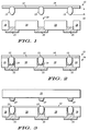
- FIG. 1 illustrates an enlarged cross-sectional view of an adhesive interposer structure or adhesive bump preform structure 11 and a printed circuit board, substrate, or base substrate 18 at an early stage of processing according to the present invention.
- Adhesive interposer structure 11 includes a non-conductive adhesive or encapsulant portion 12 and a plurality of conductive adhesive bumps, portions, or dots 13, which are coupled to non-conductive adhesive portion 12.
- Adhesive interposer structure 11 is also referred to as an adhesive bump preform or an "Area Bonding Conductive (ABC)" film adhesive.
- adhesive interposer structure 11 comprises a novolac-type resin
- it is first tacked to substrate 18 by applying a pressure on the order of 2-4 psi and heating the structure for approximately 1 to 2 seconds at about 80°C to 100°C to dry out solvent present in the resin.
- the heat may cause partial curing (or B-staging) of the resin.
- intermediate assembly structure 24 can be conveniently loaded into a carrier (e.g., a reel carrier, waffle pack, or the like) for storage.
- a carrier e.g., a reel carrier, waffle pack, or the like
- This is a significant advantage over the prior art because the manufacturer of substrate 18 for example, can apply adhesive interposer structure 11 to substrate 18, partially cure the interposer, and package the resulting intermediate assembly for shipment to a semiconductor chip supplier or manufacturer. This greatly simplifies the processing that is required of the semiconductor chip supplier.
- support film 14 is removed as shown in FIG. 3.
- support film 14 is removed before the substrate assembly is placed in a carrier device as described above.
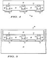
- Semiconductor device 26 includes a plurality of conductive bumps, portions, or raised portions 27 for electrically coupling to conductive metal pads 21.
- substrate module 28 is stored until it is coupled to the next level of assembly such as a card body, device, or substrate 29 shown in FIG. 5, which illustrates a simplified cross-sectional view of a smartcard device or assembly with an embedded substrate module 28.
- Substrate module 28 is conveniently stored in a tape and reel carrier or waffle pack carrier to support automation at the next level of assembly.
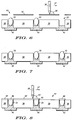
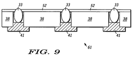
- FIGs. 6-9 illustrate enlarged cross-sectional views of an alternative method for forming a substrate structure according to the present invention.
- FIG. 6 illustrates a substrate 38 having a plurality of vias 39 and a plurality of metal contact pads 41.
- a screen mask or stencil 42 having openings 43 is used to selectively deposit or place a conductive adhesive bump 33 in each of vias 39.
- a blade device 36 is used to spread a bulk conductive adhesive material 34 across (as represented by arrow 37) screen mask 42 to selectively deposit conductive adhesive material 34 in each of vias 39 to provide the structure shown in FIG. 7.
- conductive adhesive material 34 comprises a B-stageable epoxy such as 1873-14, which is available from Merix Corporation.
Landscapes
- Wire Bonding (AREA)
- Combinations Of Printed Boards (AREA)
- Structures For Mounting Electric Components On Printed Circuit Boards (AREA)
Applications Claiming Priority (2)
| Application Number | Priority Date | Filing Date | Title |
|---|---|---|---|
| US654466 | 1996-05-28 | ||
| US08/654,466 US6022761A (en) | 1996-05-28 | 1996-05-28 | Method for coupling substrates and structure |
Publications (3)
| Publication Number | Publication Date |
|---|---|
| EP0810649A2 true EP0810649A2 (de) | 1997-12-03 |
| EP0810649A3 EP0810649A3 (de) | 1998-12-23 |
| EP0810649B1 EP0810649B1 (de) | 2003-11-05 |
Family
ID=24624967
Family Applications (1)
| Application Number | Title | Priority Date | Filing Date |
|---|---|---|---|
| EP97107710A Expired - Lifetime EP0810649B1 (de) | 1996-05-28 | 1997-05-12 | Fügemethode für Substrate und Struktur |
Country Status (4)
| Country | Link |
|---|---|
| US (1) | US6022761A (de) |
| EP (1) | EP0810649B1 (de) |
| JP (1) | JP3962449B2 (de) |
| DE (1) | DE69725926T2 (de) |
Cited By (10)
| Publication number | Priority date | Publication date | Assignee | Title |
|---|---|---|---|---|
| EP0954021A1 (de) * | 1998-04-30 | 1999-11-03 | SCHLUMBERGER Systèmes | Verfahren zum Herstellen eines elektronischen Bauelementes und elektronisches Bauelement |
| GB2339332A (en) * | 1998-07-08 | 2000-01-19 | Infrared Integrated Syst Ltd | Assembling planar electrical components |
| EP0994508A1 (de) * | 1998-10-12 | 2000-04-19 | Shinko Electric Industries Co. Ltd. | Halbleiteranordnung mit Kontakthöckern |
| WO2001075970A3 (en) * | 2000-03-31 | 2002-02-28 | Heinze Dyconex Patente | Element and method for connecting constituents of an electronic assembly |
| US6429516B1 (en) * | 1997-02-28 | 2002-08-06 | Fujitsu, Limited | Structure for mounting a bare chip using an interposer |
| EP1122781A3 (de) * | 2000-02-01 | 2003-05-02 | Mitsubishi Denki Kabushiki Kaisha | Hochdicht-montiertes Element mit Klebefolie |
| KR100392406B1 (ko) * | 1998-09-17 | 2003-07-22 | 후지쯔 가부시끼가이샤 | 반도체 시험장치 및 방법 |
| EP1137066A3 (de) * | 2000-03-24 | 2004-12-22 | Shinko Electric Industries Co. Ltd. | Halbleiter und seine Herstellung |
| FR2894070A1 (fr) * | 2005-11-30 | 2007-06-01 | 3D Plus Sa Sa | Module electronique 3d |
| EP1212791A4 (de) * | 1999-07-30 | 2008-05-28 | Micron Technology Inc | Methode und struktur für die verarbeitung von halbleitergehäusen mit hoher ausbeute |
Families Citing this family (40)
| Publication number | Priority date | Publication date | Assignee | Title |
|---|---|---|---|---|
| EP0817548B1 (de) * | 1996-01-11 | 2006-04-05 | Ibiden Co., Ltd. | Gedruckte schaltungsplatte und verfahren zu deren herstellung |
| WO1998004000A1 (fr) * | 1996-07-22 | 1998-01-29 | Honda Giken Kogyo Kabushiki Kaisha | Unite de commande electronique de type enfichable, structure de connexion entre un tableau de connexion et des fiches, unite de connexion entre des pieces electroniques et un tableau de connexion et procede de montage de pieces electroniques |
| US6981317B1 (en) * | 1996-12-27 | 2006-01-03 | Matsushita Electric Industrial Co., Ltd. | Method and device for mounting electronic component on circuit board |
| US6168972B1 (en) * | 1998-12-22 | 2001-01-02 | Fujitsu Limited | Flip chip pre-assembly underfill process |
| US6288905B1 (en) * | 1999-04-15 | 2001-09-11 | Amerasia International Technology Inc. | Contact module, as for a smart card, and method for making same |
| WO2001026147A1 (en) * | 1999-10-04 | 2001-04-12 | Seiko Epson Corporation | Semiconductor device, method of manufacture thereof, circuit board, and electronic device |
| JP3973340B2 (ja) * | 1999-10-05 | 2007-09-12 | Necエレクトロニクス株式会社 | 半導体装置、配線基板、及び、それらの製造方法 |
| KR100587389B1 (ko) * | 2000-12-23 | 2006-06-08 | 앰코 테크놀로지 코리아 주식회사 | 적층형 반도체 패키지 |
| KR100565766B1 (ko) * | 2001-01-03 | 2006-03-29 | 앰코 테크놀로지 코리아 주식회사 | 반도체 칩 패키지 및 그 제조방법 |
| US6648213B1 (en) | 2001-03-05 | 2003-11-18 | Saturn Electronics & Engineering, Inc. | Manufacturing method for attaching components to a substrate |
| US7115986B2 (en) * | 2001-05-02 | 2006-10-03 | Micron Technology, Inc. | Flexible ball grid array chip scale packages |
| US7218527B1 (en) * | 2001-08-17 | 2007-05-15 | Alien Technology Corporation | Apparatuses and methods for forming smart labels |
| SG122743A1 (en) * | 2001-08-21 | 2006-06-29 | Micron Technology Inc | Microelectronic devices and methods of manufacture |
| SG104293A1 (en) | 2002-01-09 | 2004-06-21 | Micron Technology Inc | Elimination of rdl using tape base flip chip on flex for die stacking |
| SG115459A1 (en) * | 2002-03-04 | 2005-10-28 | Micron Technology Inc | Flip chip packaging using recessed interposer terminals |
| SG115456A1 (en) | 2002-03-04 | 2005-10-28 | Micron Technology Inc | Semiconductor die packages with recessed interconnecting structures and methods for assembling the same |
| US6975035B2 (en) * | 2002-03-04 | 2005-12-13 | Micron Technology, Inc. | Method and apparatus for dielectric filling of flip chip on interposer assembly |
| SG115455A1 (en) | 2002-03-04 | 2005-10-28 | Micron Technology Inc | Methods for assembly and packaging of flip chip configured dice with interposer |
| SG111935A1 (en) * | 2002-03-04 | 2005-06-29 | Micron Technology Inc | Interposer configured to reduce the profiles of semiconductor device assemblies and packages including the same and methods |
| SG121707A1 (en) * | 2002-03-04 | 2006-05-26 | Micron Technology Inc | Method and apparatus for flip-chip packaging providing testing capability |
| US20030183332A1 (en) * | 2002-03-26 | 2003-10-02 | Simila Charles E. | Screen printed thermal expansion standoff |
| US20040036170A1 (en) * | 2002-08-20 | 2004-02-26 | Lee Teck Kheng | Double bumping of flexible substrate for first and second level interconnects |
| TW563233B (en) * | 2002-09-11 | 2003-11-21 | Advanced Semiconductor Eng | Process and structure for semiconductor package |
| US20050012225A1 (en) * | 2002-11-15 | 2005-01-20 | Choi Seung-Yong | Wafer-level chip scale package and method for fabricating and using the same |
| US6839965B2 (en) * | 2003-02-06 | 2005-01-11 | R-Tec Corporation | Method of manufacturing a resistor connector |
| DE10339609A1 (de) * | 2003-08-28 | 2005-03-24 | Forschungszentrum Karlsruhe Gmbh | Oligonukleotid, Verfahren und System zur Detektion von Antibiotikaresistenz-vermittelnden Genen in Mikroorganismen mittels der Echtzeit-PCR |
| US7208346B2 (en) * | 2004-06-14 | 2007-04-24 | David Lee | Methods of forming interposers on surfaces of dies of a wafer |
| KR100601762B1 (ko) * | 2004-11-09 | 2006-07-19 | 삼성전자주식회사 | 비전도성 접착제를 사용하는 플립 칩 본딩 제조 방법 |
| TWI261325B (en) * | 2005-03-25 | 2006-09-01 | Advanced Semiconductor Eng | Package structure of semiconductor and wafer-level formation thereof |
| US7749806B2 (en) * | 2005-09-22 | 2010-07-06 | Chipmos Technologies Inc. | Fabricating process of a chip package structure |
| US7847414B2 (en) | 2005-09-22 | 2010-12-07 | Chipmos Technologies Inc. | Chip package structure |
| US7960214B2 (en) * | 2005-09-22 | 2011-06-14 | Chipmos Technologies Inc. | Chip package |
| US7651758B2 (en) * | 2005-10-18 | 2010-01-26 | Endres Machining Innovations Llc | System for improving the wearability of a surface and related method |
| TWI299554B (en) * | 2006-06-21 | 2008-08-01 | Advanced Semiconductor Eng | Substrate structure and method for manufacturing the same |
| US20090159709A1 (en) * | 2007-12-24 | 2009-06-25 | Dynamics Inc. | Advanced dynamic credit cards |
| US7666709B1 (en) * | 2008-12-10 | 2010-02-23 | Stats Chippac, Ltd. | Semiconductor device and method of placing semiconductor die on a temporary carrier using fiducial patterns |
| US8603862B2 (en) * | 2010-05-14 | 2013-12-10 | International Business Machines Corporation | Precise-aligned lock-and-key bonding structures |
| JP5686009B2 (ja) * | 2011-03-18 | 2015-03-18 | 富士通株式会社 | 基板ユニット、及び、基板ユニットの製造方法 |
| IT201700073501A1 (it) * | 2017-06-30 | 2018-12-30 | St Microelectronics Srl | Prodotto a semiconduttore e corrispondente procedimento |
| US20210103949A1 (en) | 2019-10-06 | 2021-04-08 | Dynamics Inc. | Scalable loyalty processing apparatus and methods of processing loyalty data |
Family Cites Families (16)
| Publication number | Priority date | Publication date | Assignee | Title |
|---|---|---|---|---|
| US4067104A (en) * | 1977-02-24 | 1978-01-10 | Rockwell International Corporation | Method of fabricating an array of flexible metallic interconnects for coupling microelectronics components |
| US4427715A (en) * | 1978-07-03 | 1984-01-24 | National Semiconductor Corporation | Method of forming expanded pad structure |
| JPS58215057A (ja) * | 1982-06-09 | 1983-12-14 | Hitachi Ltd | バンプ形成装置 |
| JPS595637A (ja) * | 1982-07-02 | 1984-01-12 | Hitachi Ltd | 半導体素子の実装構造および実装方法 |
| JPS601849A (ja) * | 1983-06-17 | 1985-01-08 | Sharp Corp | 電子部品の接続方法 |
| FR2584235B1 (fr) * | 1985-06-26 | 1988-04-22 | Bull Sa | Procede de montage d'un circuit integre sur un support, dispositif en resultant et son application a une carte a microcircuits electroniques |
| JPS63150931A (ja) * | 1986-12-15 | 1988-06-23 | Nec Corp | 半導体装置 |
| US5014111A (en) * | 1987-12-08 | 1991-05-07 | Matsushita Electric Industrial Co., Ltd. | Electrical contact bump and a package provided with the same |
| US5504035A (en) * | 1989-08-28 | 1996-04-02 | Lsi Logic Corporation | Process for solder ball interconnecting a semiconductor device to a substrate using a noble metal foil embedded interposer substrate |
| FR2653601B1 (fr) * | 1989-10-20 | 1993-10-22 | Sgs Thomson Microelectronics Sa | Electronique portable connectable a puces. |
| US5074947A (en) * | 1989-12-18 | 1991-12-24 | Epoxy Technology, Inc. | Flip chip technology using electrically conductive polymers and dielectrics |
| US5086558A (en) * | 1990-09-13 | 1992-02-11 | International Business Machines Corporation | Direct attachment of semiconductor chips to a substrate with a substrate with a thermoplastic interposer |
| US5667884A (en) * | 1993-04-12 | 1997-09-16 | Bolger; Justin C. | Area bonding conductive adhesive preforms |
| DE4325458A1 (de) * | 1993-07-29 | 1995-02-09 | Orga Bond Technik Gmbh | Trägerelement für einen IC-Baustein |
| US5548091A (en) * | 1993-10-26 | 1996-08-20 | Tessera, Inc. | Semiconductor chip connection components with adhesives and methods for bonding to the chip |
| KR0146063B1 (ko) * | 1995-03-28 | 1998-08-01 | 문정환 | 반도체 패키지 및 그 제조방법 |
-
1996
- 1996-05-28 US US08/654,466 patent/US6022761A/en not_active Expired - Lifetime
-
1997
- 1997-05-12 DE DE69725926T patent/DE69725926T2/de not_active Expired - Fee Related
- 1997-05-12 EP EP97107710A patent/EP0810649B1/de not_active Expired - Lifetime
- 1997-05-15 JP JP14327697A patent/JP3962449B2/ja not_active Expired - Fee Related
Cited By (16)
| Publication number | Priority date | Publication date | Assignee | Title |
|---|---|---|---|---|
| US6429516B1 (en) * | 1997-02-28 | 2002-08-06 | Fujitsu, Limited | Structure for mounting a bare chip using an interposer |
| EP0954021A1 (de) * | 1998-04-30 | 1999-11-03 | SCHLUMBERGER Systèmes | Verfahren zum Herstellen eines elektronischen Bauelementes und elektronisches Bauelement |
| FR2778308A1 (fr) * | 1998-04-30 | 1999-11-05 | Schlumberger Systems & Service | Procede de realisation d'un composant electronique et composant electronique |
| US6281048B1 (en) | 1998-04-30 | 2001-08-28 | Schlumberger Systemes | Method of making an electronic component, and an electronic component |
| GB2339332B (en) * | 1998-07-08 | 2000-07-26 | Infrared Integrated Syst Ltd | Processes for assembly of planar electrical components |
| GB2339332A (en) * | 1998-07-08 | 2000-01-19 | Infrared Integrated Syst Ltd | Assembling planar electrical components |
| KR100392406B1 (ko) * | 1998-09-17 | 2003-07-22 | 후지쯔 가부시끼가이샤 | 반도체 시험장치 및 방법 |
| EP0994508A1 (de) * | 1998-10-12 | 2000-04-19 | Shinko Electric Industries Co. Ltd. | Halbleiteranordnung mit Kontakthöckern |
| US6344695B1 (en) | 1998-10-12 | 2002-02-05 | Shinko Electric Industries Co., Ltd. | Semiconductor device to be mounted on main circuit board and process for manufacturing same device |
| EP1212791A4 (de) * | 1999-07-30 | 2008-05-28 | Micron Technology Inc | Methode und struktur für die verarbeitung von halbleitergehäusen mit hoher ausbeute |
| EP1122781A3 (de) * | 2000-02-01 | 2003-05-02 | Mitsubishi Denki Kabushiki Kaisha | Hochdicht-montiertes Element mit Klebefolie |
| EP1137066A3 (de) * | 2000-03-24 | 2004-12-22 | Shinko Electric Industries Co. Ltd. | Halbleiter und seine Herstellung |
| WO2001075970A3 (en) * | 2000-03-31 | 2002-02-28 | Heinze Dyconex Patente | Element and method for connecting constituents of an electronic assembly |
| FR2894070A1 (fr) * | 2005-11-30 | 2007-06-01 | 3D Plus Sa Sa | Module electronique 3d |
| WO2007063113A1 (fr) * | 2005-11-30 | 2007-06-07 | 3D Plus | Module electronique 3d |
| US8264853B2 (en) | 2005-11-30 | 2012-09-11 | 3D Plus | 3D electronic module |
Also Published As
| Publication number | Publication date |
|---|---|
| DE69725926T2 (de) | 2004-05-06 |
| EP0810649A3 (de) | 1998-12-23 |
| US6022761A (en) | 2000-02-08 |
| DE69725926D1 (de) | 2003-12-11 |
| JPH1070362A (ja) | 1998-03-10 |
| JP3962449B2 (ja) | 2007-08-22 |
| EP0810649B1 (de) | 2003-11-05 |
Similar Documents
| Publication | Publication Date | Title |
|---|---|---|
| US6022761A (en) | Method for coupling substrates and structure | |
| US5949142A (en) | Chip size package and method of manufacturing the same | |
| KR950012658B1 (ko) | 반도체 칩 실장방법 및 기판 구조체 | |
| US5147210A (en) | Polymer film interconnect | |
| US6821878B2 (en) | Area-array device assembly with pre-applied underfill layers on printed wiring board | |
| US6541872B1 (en) | Multi-layered adhesive for attaching a semiconductor die to a substrate | |
| KR100265616B1 (ko) | 도전성 폴리머 및 유전체를 이용한 플립칩 | |
| US5742100A (en) | Structure having flip-chip connected substrates | |
| US5747101A (en) | Direct chip attachment (DCA) with electrically conductive adhesives | |
| US6905961B2 (en) | Land grid array stiffener for use with flexible chip carriers | |
| US6331679B1 (en) | Multi-layer circuit board using anisotropic electro-conductive adhesive layer | |
| US7981725B2 (en) | Fabricating process of a chip package structure | |
| KR20010072583A (ko) | 적층화 집적 회로 패키지 | |
| US5972739A (en) | Method of manufacturing a tab semiconductor device | |
| US6528889B1 (en) | Electronic circuit device having adhesion-reinforcing pattern on a circuit board for flip-chip mounting an IC chip | |
| US5303862A (en) | Single step electrical/mechanical connection process for connecting I/O pins and creating multilayer structures | |
| KR100295731B1 (ko) | 전자패키지의제조방법 | |
| US6544818B2 (en) | Method of manufacturing semiconductor device | |
| US7960214B2 (en) | Chip package | |
| US20090079068A1 (en) | Methods for attaching a flip chip integrated circuit assembly to a substrate | |
| JPH03129745A (ja) | 半導体装置の実装方法 | |
| JP4635836B2 (ja) | シート状電子回路モジュール | |
| JP3457547B2 (ja) | 半導体装置およびその製造方法ならびにフィルムキャリア | |
| JPH09139560A (ja) | 回路基板装置およびその製造方法 | |
| KR100650492B1 (ko) | 플립칩의 실장구조 및 그 실장방법 |
Legal Events
| Date | Code | Title | Description |
|---|---|---|---|
| PUAI | Public reference made under article 153(3) epc to a published international application that has entered the european phase |
Free format text: ORIGINAL CODE: 0009012 |
|
| AK | Designated contracting states |
Kind code of ref document: A2 Designated state(s): DE FR IT NL |
|
| PUAL | Search report despatched |
Free format text: ORIGINAL CODE: 0009013 |
|
| AK | Designated contracting states |
Kind code of ref document: A3 Designated state(s): DE FR IT NL |
|
| 17P | Request for examination filed |
Effective date: 19990623 |
|
| 17Q | First examination report despatched |
Effective date: 20000809 |
|
| GRAH | Despatch of communication of intention to grant a patent |
Free format text: ORIGINAL CODE: EPIDOS IGRA |
|
| GRAS | Grant fee paid |
Free format text: ORIGINAL CODE: EPIDOSNIGR3 |
|
| GRAA | (expected) grant |
Free format text: ORIGINAL CODE: 0009210 |
|
| AK | Designated contracting states |
Kind code of ref document: B1 Designated state(s): DE FR IT NL |
|
| REF | Corresponds to: |
Ref document number: 69725926 Country of ref document: DE Date of ref document: 20031211 Kind code of ref document: P |
|
| ET | Fr: translation filed | ||
| PLBE | No opposition filed within time limit |
Free format text: ORIGINAL CODE: 0009261 |
|
| STAA | Information on the status of an ep patent application or granted ep patent |
Free format text: STATUS: NO OPPOSITION FILED WITHIN TIME LIMIT |
|
| 26N | No opposition filed |
Effective date: 20040806 |
|
| NLS | Nl: assignments of ep-patents |
Owner name: FREESCALE SEMICONDUCTOR, INC. Effective date: 20051028 |
|
| PGFP | Annual fee paid to national office [announced via postgrant information from national office to epo] |
Ref country code: IT Payment date: 20060531 Year of fee payment: 10 |
|
| REG | Reference to a national code |
Ref country code: FR Ref legal event code: TP |
|
| PGFP | Annual fee paid to national office [announced via postgrant information from national office to epo] |
Ref country code: DE Payment date: 20080530 Year of fee payment: 12 |
|
| PGFP | Annual fee paid to national office [announced via postgrant information from national office to epo] |
Ref country code: NL Payment date: 20080410 Year of fee payment: 12 |
|
| PG25 | Lapsed in a contracting state [announced via postgrant information from national office to epo] |
Ref country code: IT Free format text: LAPSE BECAUSE OF NON-PAYMENT OF DUE FEES Effective date: 20070512 |
|
| NLV4 | Nl: lapsed or anulled due to non-payment of the annual fee |
Effective date: 20091201 |
|
| PG25 | Lapsed in a contracting state [announced via postgrant information from national office to epo] |
Ref country code: NL Free format text: LAPSE BECAUSE OF NON-PAYMENT OF DUE FEES Effective date: 20091201 |
|
| REG | Reference to a national code |
Ref country code: FR Ref legal event code: ST Effective date: 20100129 |
|
| PG25 | Lapsed in a contracting state [announced via postgrant information from national office to epo] |
Ref country code: FR Free format text: LAPSE BECAUSE OF NON-PAYMENT OF DUE FEES Effective date: 20090602 |
|
| PGFP | Annual fee paid to national office [announced via postgrant information from national office to epo] |
Ref country code: FR Payment date: 20080424 Year of fee payment: 12 |
|
| PG25 | Lapsed in a contracting state [announced via postgrant information from national office to epo] |
Ref country code: DE Free format text: LAPSE BECAUSE OF NON-PAYMENT OF DUE FEES Effective date: 20091201 |