EP0810733A2 - IC für den Betrieb bei unterschiedlichen Versorgungsspannungen - Google Patents
IC für den Betrieb bei unterschiedlichen Versorgungsspannungen Download PDFInfo
- Publication number
- EP0810733A2 EP0810733A2 EP97303436A EP97303436A EP0810733A2 EP 0810733 A2 EP0810733 A2 EP 0810733A2 EP 97303436 A EP97303436 A EP 97303436A EP 97303436 A EP97303436 A EP 97303436A EP 0810733 A2 EP0810733 A2 EP 0810733A2
- Authority
- EP
- European Patent Office
- Prior art keywords
- power
- input buffer
- input
- threshold
- buffer
- Prior art date
- Legal status (The legal status is an assumption and is not a legal conclusion. Google has not performed a legal analysis and makes no representation as to the accuracy of the status listed.)
- Withdrawn
Links
Images

Classifications
-
- G—PHYSICS
- G11—INFORMATION STORAGE
- G11C—STATIC STORES
- G11C7/00—Arrangements for writing information into, or reading information out from, a digital store
-
- H—ELECTRICITY
- H03—ELECTRONIC CIRCUITRY
- H03K—PULSE TECHNIQUE
- H03K19/00—Logic circuits, i.e. having at least two inputs acting on one output; Inverting circuits
- H03K19/0021—Modifications of threshold
- H03K19/0027—Modifications of threshold in field effect transistor circuits
-
- H—ELECTRICITY
- H03—ELECTRONIC CIRCUITRY
- H03K—PULSE TECHNIQUE
- H03K19/00—Logic circuits, i.e. having at least two inputs acting on one output; Inverting circuits
- H03K19/0175—Coupling arrangements; Interface arrangements
- H03K19/0185—Coupling arrangements; Interface arrangements using field effect transistors only
- H03K19/018585—Coupling arrangements; Interface arrangements using field effect transistors only programmable
Definitions
- the present invention relates to a multiple-power IC device such as a multiple-power semiconductor integrated circuit which has an input buffer compatible with a plurality of powers.
- the input terminal of a semiconductor IC device has an input buffer which functions as an interface.
- This input buffer allows signals to be sent from the input terminal to the internal circuit of an semiconductor IC device based on a threshold according to the voltage supplied to the input buffer.
- This type of IC device is usually built on a printed circuit board.
- a printed circuit board to be used as a TTL logic circuit two types of power, 3V and 5V, are supplied in most cases. And, depending upon the environment in which this IC device is used, a 3V or 5V power is selected for use in the input buffer of the IC device built on the circuit board.
- CMOS Complementary Metal Oxide Semiconductor
- this CMOS buffer Upon receiving an input signal, this CMOS buffer sends an output signal to the internal circuit according to its threshold.
- This threshold is determined by two factors: one is the ratio between the p-channel MOSFET gate width and the n-channel MOSFET gate width of the CMOS buffer and the other is the voltage of the power supplied to the buffer. And, by matching the threshold of this buffer to the median between the L (low) level and the H (high) level of the input signal, a sufficient noise margin is provided for each of both the L level and the H level of the input signal.
- the buffer when a TTL-level signal with an amplitude of about 3V is sent to the buffer with the power voltage of 5V and when the threshold of the buffer is 1.5V which is about the median of the input signal level, it is possible for the buffer to match threshold to the median of the L level and H level of the input signal. In this case, a sufficient margin is provided for each of the L level noise and the H level noise.
- the threshold of the conventional multiple-power IC circuit varies according to the driving power of the input buffer, resulting in a variation in the input signal noise margin.
- the present invention has the following configuration.
- a multiple-power IC device comprises: an input buffer to which one of a plurality of power voltages may be applied; an internal circuit connected to the input buffer; and a switching terminal connected to, and controlling, the input buffer, wherein the input buffer sends output signals, corresponding to input signals, to the internal circuit according to a threshold and wherein the switching circuit holds the threshold of the input buffer at a desired voltage level regardless of the power voltage applied to the input buffer.
- a multiple-power IC device has the switching circuit set the threshold of the input buffer to an appropriate value, regardless of the voltage to be applied. This prevents the threshold from being changed even if the power voltage changes.
- the threshold is not affected by, and the input signal noise margin is not subject to, the selected power voltage.
- the threshold should be set approximately to the median between the L level and the H level of the input signal.
- the present invention is most suited to a multiple-power IC device to which TTL level signals are sent.
- the switching circuit may have a power voltage determination circuit, which checks the power voltage to control the input buffer operation automatically.
- the input buffer may comprise a plurality of input buffers. Upon receiving input signals, each buffer is capable of generating signals, with the same threshold, regardless of the differences among the power voltage levels.
- the switching circuit selects one of the input buffers according to the power voltage, thus preventing the threshold from being changed.
- the input buffer may comprise a CMOS buffer which comprises a p-channel MOSFET with a gate and an n-channel MOSFET with a gate and connected in series with the p-channel MOSFET; and an auxiliary MOSFET with a gate and with the same type of channel as that of one of the MOSFETs connected in parallel.
- CMOS buffer which comprises a p-channel MOSFET with a gate and an n-channel MOSFET with a gate and connected in series with the p-channel MOSFET; and an auxiliary MOSFET with a gate and with the same type of channel as that of one of the MOSFETs connected in parallel.
- the switching circuit turns on or off the voltage to be applied to the gate of the auxiliary MOSFET. Turning on or off the voltage of the gate of the auxiliary MOSFET effectively changes the gate width ratio between both MOSFETs constituting the CMOS buffer. A change in the gate width ratio allows the threshold of the input buffer to be fixed regardless of the power voltage.
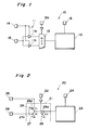
- Fig. 1 is a circuit diagram showing the first embodiment of the multiple-power IC device according to the present invention.
- Fig. 2 is a circuit diagram showing the second embodiment of the multiple-power IC device according to the present invention.
- Fig. 3 is a circuit diagram showing the third embodiment of the multiple-power IC device according to the present invention.
- Fig. 4 is a circuit diagram showing the fourth embodiment of the multiple-power IC device according to the present invention.
- Fig. 1 is a circuit diagram showing the first embodiment of the multiple-power IC device according to the present invention.
- the ground (GND) terminal and its associated wiring are not included in the figure.
- the multiple-power IC device 10 comprises the input buffers 11 (11a and 11b), switching circuit 12 for selecting one of the input buffers, and internal circuit 13 to which signals are sent from the input buffer 11.
- the multiple-power IC device 10 is built on a printed circuit board (not shown in the figure) to which one of two power voltages, for example, 3V and 5V, is supplied.
- the input buffer 11 typically comprises two CMOS buffers, 11a and 11b.
- the threshold is set to 1.5V which is the median of the TTL-level signal amplitude.
- the 3V power is applied to the other CMOS buffer, 11b, its threshold is set to 1.5V which is the same as that of the CMOS buffer 11a.
- the 3V or 5V power is supplied to the power voltage terminal 14 and, via that terminal, the 3V or 5V power voltage is supplied to the buffers 11a and 11b.
- TTL-level signals are sent to the buffers 11a and 11b via the common signal input terminal 15.
- the multiplexer 12 On the output side of the buffers 11a and 11b is provided the multiplexer 12 which connects these buffers to the internal circuit 13.
- the internal circuit 13 shown in the figure operates, for example, on the 3V power supplied to the power terminal 16.
- the multiplexer 12 located between the input buffer 11 and the internal circuit 13 comprises the switching circuit (MUX) sending signals from the buffers 11a or 11b to the internal circuit 13 as determined by the switching operation terminal 12a.
- MUX switching circuit
- the switching operation terminal 12a selects one of the buffers, 11a or 11b, according to the environment in which the circuit board containing the IC is used. That is, when the 5V power is selected for the input buffer 11, the switching operation terminal 12a selects the buffer 11a which is set up as a 5V TTL buffer; when the 3V power is selected for the input buffer 11, the switching operation terminal 12a selects the buffer 11b which is set up as a 3V TTL buffer. This allows the switching circuit12 to select the buffer 11a or 11b with an appropriate threshold according to the power voltage, thus always ensuring the effective TTL-level signal threshold of 1.5V.
- the multiple-power IC device 10 always sets the threshold to the median of the input signal amplitude regardless of which power voltage is selected, This makes the optimum noise margins always available for both the L level noises and H level noises of the input signals.
- the multiple-power IC device 20 comprises the input buffer 21, terminal 22 for controlling the operation of the input buffer 21, and internal circuit 23 to which signals are sent from the input buffer 21.
- the multiple-power IC device 20 is built on a printed circuit board (not shown in the figure) to which one of two power voltages, for example, 3V and 5V, is supplied for TTL-level signals.
- the internal circuit 23 operates, for example, on the 3V power applied to the power terminal 24.
- the input buffer 21 from which signals are sent to the internal circuit 23 has the p-channel MOSFET 26 and n-channel MOSFET 27, connected in series, between the power voltage terminal 25 and the ground, as in the conventional CMOS buffer.
- the inverted input signal is sent from the signal input terminal 28 to the gate 26a at the input of the MOSFET 26; the non-inverted input signal is sent from the signal input terminal 28 to the gate 27a at the input of the MOSFET 27.
- the n-channel MOSFET 27 is connected in parallel with the auxiliary n-channel MOSFET 29.
- the terminal 22 is connected to the gate 29a of this auxiliary MOSFET 29.
- This terminal 22 has the means for applying a gate voltage to the auxiliary MOSFET 29 to turn it on.
- turning off the gate voltage to the auxiliary MOSFET 29 turns off the auxiliary MOSFET 29. Therefore, turning on or off the gate voltage applied to the terminal 22 turns on or off the auxiliary MOSFET 29.
- the gate width ratio in the input buffer 21, that is, the gate width ratio between the MOSFET 26 and the MOSFET 27, is represented as Wp : Wn1, where Wp is the gate width of the p-channel MOSFET 26 and Wn1 is the gate width of the n-channel MOSFET 27.
- Wp the gate width ratio in the input buffer 21
- Wn the gate width ratio in the input buffer 21
- the threshold of the input buffer 21 with the auxiliary MOSFET 29 turned on is 1.5V; when the 3V power is supplied to terminal 25, the threshold of the input buffer 21 with the auxiliary MOSFET 29 turned off is 1.5V regardless of a variation in the power voltage.
- Fig. 2 shows the multiple-power IC device 20 containing the n-channel MOSFET 27 and the auxiliary MOSFET 29 connected in parallel.
- the p-channel MOSFET 26 may be connected in parallel with another p-channel MOSFET which functions as an auxiliary MOSFET.
- the multiple-power IC device 30 shown in Fig. 3 comprises the multiple-power IC device shown in the first embodiment plus the power voltage determination circuit 31.
- the power voltage determination circuit 31 activates the switching circuit12 according to the applied voltage. More specifically, upon detecting that the 5V power is supplied to the CMOS buffers 11a and 11b, the switching circuit12 selects the input buffer 11a for the 5V TTL signals and, upon detecting that the 3V power is supplied, selects the CMOS buffer 11b for 3V TTL signals.
- the multiple-power IC device 30 eliminates the need for manually operating the switching operation terminal 12a. Instead, regardless of whether the voltage of the power voltage terminal 14 is 3V or 5V, the power voltage determination circuit 31 automatically determines the voltage to assign the input buffer 11 an appropriate threshold value. This prevents setting errors on the switching operation terminal 12a, such as those caused by the operator, and also prevents variations in the noise margins introduced by setting errors.
- the multiple-power IC device 40 shown in Fig. 4 comprises the multiple-power IC device shown in the second embodiment plus the power voltage determination circuit 41.
- the power voltage terminal 25 applies a voltage to the power voltage determination circuit 41.
- the power voltage determination circuit 41 checks the voltage applied by the power voltage terminal 25 to control the gate voltage application terminal 22, which functions as the switching circuit, according to the applied voltage. More specifically, upon detecting that the 5V power is supplied from the power voltage terminal 25 to activate the input buffer 21, the terminal 22 turns on the auxiliary MOSFET 29 to make the input buffer 21 available for use as the 5V TTL buffer.
- the multiple-power IC device 40 uses the power voltage determination circuit 41 to determine the voltage automatically and assigns the input buffer 11 an appropriate threshold value. This prevents setting errors as well as variations in the noise margins introduced by setting errors.
- the multiple-power IC device has the switching circuit to set the threshold of the input buffer to an appropriate value, regardless of the voltage to be applied. This allows the input buffer to have a fixed threshold regardless of the differences among the voltage to be applied to the input buffer. This, in turn, allows the multiple-power IC device to have a constant input signal noise margin.
Landscapes
- Engineering & Computer Science (AREA)
- Computer Hardware Design (AREA)
- Physics & Mathematics (AREA)
- Computing Systems (AREA)
- General Engineering & Computer Science (AREA)
- Mathematical Physics (AREA)
- Logic Circuits (AREA)
- Semiconductor Integrated Circuits (AREA)
- Dram (AREA)
Applications Claiming Priority (2)
| Application Number | Priority Date | Filing Date | Title |
|---|---|---|---|
| JP8133373A JPH09321603A (ja) | 1996-05-28 | 1996-05-28 | 多電源半導体集積回路 |
| JP133373/96 | 1996-05-28 |
Publications (2)
| Publication Number | Publication Date |
|---|---|
| EP0810733A2 true EP0810733A2 (de) | 1997-12-03 |
| EP0810733A3 EP0810733A3 (de) | 1998-08-19 |
Family
ID=15103219
Family Applications (1)
| Application Number | Title | Priority Date | Filing Date |
|---|---|---|---|
| EP97303436A Withdrawn EP0810733A3 (de) | 1996-05-28 | 1997-05-20 | IC für den Betrieb bei unterschiedlichen Versorgungsspannungen |
Country Status (6)
| Country | Link |
|---|---|
| US (1) | US6034550A (de) |
| EP (1) | EP0810733A3 (de) |
| JP (1) | JPH09321603A (de) |
| KR (1) | KR970076811A (de) |
| CN (1) | CN1167372A (de) |
| TW (1) | TW399367B (de) |
Families Citing this family (6)
| Publication number | Priority date | Publication date | Assignee | Title |
|---|---|---|---|---|
| US6380762B1 (en) * | 1997-03-27 | 2002-04-30 | Cypress Semiconductor Corporation | Multi-level programmable voltage control and output buffer with selectable operating voltage |
| JP2006013166A (ja) * | 2004-06-25 | 2006-01-12 | Sharp Corp | 発光ダイオード駆動回路、及びそれを備えた光送信デバイス、並びに電子機器 |
| KR100743624B1 (ko) * | 2004-12-29 | 2007-07-27 | 주식회사 하이닉스반도체 | 전력 소모를 줄인 반도체 장치 |
| KR100610020B1 (ko) * | 2005-01-13 | 2006-08-08 | 삼성전자주식회사 | 반도체 메모리 장치에서의 셀 파워 스위칭 회로와 그에따른 셀 파워 전압 인가방법 |
| US7770037B2 (en) * | 2006-04-20 | 2010-08-03 | Advanced Micro Devices, Inc. | Power ok distribution for multi-voltage chips |
| US10033388B1 (en) * | 2017-03-21 | 2018-07-24 | Xilinx, Inc. | Circuit for and method of enabling the selection of a circuit |
Family Cites Families (12)
| Publication number | Priority date | Publication date | Assignee | Title |
|---|---|---|---|---|
| KR910005609B1 (ko) * | 1988-07-19 | 1991-07-31 | 삼성전자 주식회사 | 복수전압 ic용 입력신호 로직 판별회로 |
| JPH07114359B2 (ja) * | 1989-07-28 | 1995-12-06 | 株式会社東芝 | 半導体集積回路 |
| IT1243676B (it) * | 1990-07-19 | 1994-06-21 | Sgs Thomson Microelectronics | Stadio d'ingresso pluricompatibile particolarmente per porte logiche in circuiti integrati |
| JP2758259B2 (ja) * | 1990-09-27 | 1998-05-28 | 株式会社東芝 | バッファ回路 |
| EP0590326A1 (de) * | 1992-09-29 | 1994-04-06 | Siemens Aktiengesellschaft | CMOS-Eingangsstufe |
| US5341045A (en) * | 1992-11-06 | 1994-08-23 | Intel Corporation | Programmable input buffer |
| US5430400A (en) * | 1993-08-03 | 1995-07-04 | Schlumberger Technologies Inc. | Driver circuits for IC tester |
| KR0130037B1 (ko) * | 1993-12-18 | 1998-04-06 | 김광호 | 동작전압의 변동에 대응 가능한 반도체집적회로의 입력버퍼회로 |
| US5477172A (en) * | 1994-12-12 | 1995-12-19 | Advanced Micro Devices, Inc. | Configurable input buffer dependent on supply voltage |
| US5668483A (en) * | 1995-06-21 | 1997-09-16 | Micron Quantum Devices, Inc. | CMOS buffer having stable threshold voltage |
| KR0157886B1 (ko) * | 1995-07-22 | 1999-03-20 | 문정환 | 반도체 메모리의 입력 버퍼 회로 |
| US5801548A (en) * | 1996-04-11 | 1998-09-01 | Xilinx Inc | Configurable performance-optimized programmable logic device |
-
1996
- 1996-05-28 JP JP8133373A patent/JPH09321603A/ja not_active Withdrawn
-
1997
- 1997-05-20 EP EP97303436A patent/EP0810733A3/de not_active Withdrawn
- 1997-05-22 US US08/861,623 patent/US6034550A/en not_active Expired - Fee Related
- 1997-05-24 TW TW086107016A patent/TW399367B/zh not_active IP Right Cessation
- 1997-05-26 CN CN97105525A patent/CN1167372A/zh active Pending
- 1997-05-26 KR KR1019970020743A patent/KR970076811A/ko not_active Withdrawn
Also Published As
| Publication number | Publication date |
|---|---|
| JPH09321603A (ja) | 1997-12-12 |
| US6034550A (en) | 2000-03-07 |
| KR970076811A (ko) | 1997-12-12 |
| CN1167372A (zh) | 1997-12-10 |
| EP0810733A3 (de) | 1998-08-19 |
| TW399367B (en) | 2000-07-21 |
Similar Documents
| Publication | Publication Date | Title |
|---|---|---|
| US6040714A (en) | Method for providing two modes of I/O pad termination | |
| EP0768671A2 (de) | Schaltungen, Systeme und Verfahren zur Reduzierung der Verlustleistung während einer Datenübertragung in einer stromführenden Leitung | |
| US20010012190A1 (en) | Input stage protection circuit for a receiver | |
| US6970024B1 (en) | Over-voltage protection of integrated circuit I/O pins | |
| EP0258808B1 (de) | Integrierte komplementäre MOS-Schaltung | |
| US6037803A (en) | Integrated circuit having two modes of I/O pad termination | |
| US6034550A (en) | Multi-power IC device | |
| US7368951B2 (en) | Data transmission circuit and data transmission method with two transmission modes | |
| US7378896B2 (en) | Single pin for multiple functional control purposes | |
| CA2302939C (en) | Variable impedance data transmission device | |
| US6956401B1 (en) | Differential input buffers with elevated power supplies | |
| JP4054727B2 (ja) | 出力バッファ回路及び出力バッファ回路を使用したインタフェース回路 | |
| US5914617A (en) | Output driver for sub-micron CMOS | |
| US6480051B2 (en) | Voltage supply discriminator and method | |
| US4894558A (en) | Power saving input buffer for use with a gate array | |
| US6496036B2 (en) | Input-output buffer circuit | |
| US20030141895A1 (en) | Programmable termination for CML I/O | |
| US5819099A (en) | Voltage converting I/O driver circuit | |
| US6456147B1 (en) | Output interface circuit | |
| US6239617B1 (en) | Mixed voltage output driver with automatic impedance adjustment | |
| US11652476B2 (en) | Pad-tracking circuit design to prevent leakage current during power ramp up or ramp down of output buffer | |
| JPH06268505A (ja) | 半導体集積回路 | |
| JP2001339285A (ja) | パワーオフ検出回路 | |
| JP3923397B2 (ja) | レベルトランスレータ回路 | |
| JP2500775B2 (ja) | 半導体集積回路 |
Legal Events
| Date | Code | Title | Description |
|---|---|---|---|
| PUAI | Public reference made under article 153(3) epc to a published international application that has entered the european phase |
Free format text: ORIGINAL CODE: 0009012 |
|
| AK | Designated contracting states |
Kind code of ref document: A2 Designated state(s): DE FR GB NL |
|
| PUAL | Search report despatched |
Free format text: ORIGINAL CODE: 0009013 |
|
| AK | Designated contracting states |
Kind code of ref document: A3 Designated state(s): DE FR GB NL |
|
| STAA | Information on the status of an ep patent application or granted ep patent |
Free format text: STATUS: THE APPLICATION IS DEEMED TO BE WITHDRAWN |
|
| 18D | Application deemed to be withdrawn |
Effective date: 19990220 |