EP0813245A2 - Aluminium-Zwischenverbindungen - Google Patents
Aluminium-Zwischenverbindungen Download PDFInfo
- Publication number
- EP0813245A2 EP0813245A2 EP97303858A EP97303858A EP0813245A2 EP 0813245 A2 EP0813245 A2 EP 0813245A2 EP 97303858 A EP97303858 A EP 97303858A EP 97303858 A EP97303858 A EP 97303858A EP 0813245 A2 EP0813245 A2 EP 0813245A2
- Authority
- EP
- European Patent Office
- Prior art keywords
- aluminum
- oxide
- layer
- insulator layer
- surface roughness
- Prior art date
- Legal status (The legal status is an assumption and is not a legal conclusion. Google has not performed a legal analysis and makes no representation as to the accuracy of the status listed.)
- Withdrawn
Links
Images


Classifications
-
- H—ELECTRICITY
- H10—SEMICONDUCTOR DEVICES; ELECTRIC SOLID-STATE DEVICES NOT OTHERWISE PROVIDED FOR
- H10W—GENERIC PACKAGES, INTERCONNECTIONS, CONNECTORS OR OTHER CONSTRUCTIONAL DETAILS OF DEVICES COVERED BY CLASS H10
- H10W20/00—Interconnections in chips, wafers or substrates
- H10W20/40—Interconnections external to wafers or substrates, e.g. back-end-of-line [BEOL] metallisations or vias connecting to gate electrodes
- H10W20/41—Interconnections external to wafers or substrates, e.g. back-end-of-line [BEOL] metallisations or vias connecting to gate electrodes characterised by their conductive parts
- H10W20/44—Conductive materials thereof
- H10W20/4403—Conductive materials thereof based on metals, e.g. alloys, metal silicides
- H10W20/4405—Conductive materials thereof based on metals, e.g. alloys, metal silicides the principal metal being aluminium
- H10W20/4407—Aluminium alloys
-
- H—ELECTRICITY
- H10—SEMICONDUCTOR DEVICES; ELECTRIC SOLID-STATE DEVICES NOT OTHERWISE PROVIDED FOR
- H10W—GENERIC PACKAGES, INTERCONNECTIONS, CONNECTORS OR OTHER CONSTRUCTIONAL DETAILS OF DEVICES COVERED BY CLASS H10
- H10W20/00—Interconnections in chips, wafers or substrates
- H10W20/01—Manufacture or treatment
- H10W20/031—Manufacture or treatment of conductive parts of the interconnections
-
- H—ELECTRICITY
- H10—SEMICONDUCTOR DEVICES; ELECTRIC SOLID-STATE DEVICES NOT OTHERWISE PROVIDED FOR
- H10W—GENERIC PACKAGES, INTERCONNECTIONS, CONNECTORS OR OTHER CONSTRUCTIONAL DETAILS OF DEVICES COVERED BY CLASS H10
- H10W20/00—Interconnections in chips, wafers or substrates
- H10W20/01—Manufacture or treatment
- H10W20/071—Manufacture or treatment of dielectric parts thereof
-
- H—ELECTRICITY
- H10—SEMICONDUCTOR DEVICES; ELECTRIC SOLID-STATE DEVICES NOT OTHERWISE PROVIDED FOR
- H10W—GENERIC PACKAGES, INTERCONNECTIONS, CONNECTORS OR OTHER CONSTRUCTIONAL DETAILS OF DEVICES COVERED BY CLASS H10
- H10W20/00—Interconnections in chips, wafers or substrates
- H10W20/01—Manufacture or treatment
- H10W20/071—Manufacture or treatment of dielectric parts thereof
- H10W20/092—Manufacture or treatment of dielectric parts thereof by smoothing the dielectric parts
-
- Y—GENERAL TAGGING OF NEW TECHNOLOGICAL DEVELOPMENTS; GENERAL TAGGING OF CROSS-SECTIONAL TECHNOLOGIES SPANNING OVER SEVERAL SECTIONS OF THE IPC; TECHNICAL SUBJECTS COVERED BY FORMER USPC CROSS-REFERENCE ART COLLECTIONS [XRACs] AND DIGESTS
- Y10—TECHNICAL SUBJECTS COVERED BY FORMER USPC
- Y10S—TECHNICAL SUBJECTS COVERED BY FORMER USPC CROSS-REFERENCE ART COLLECTIONS [XRACs] AND DIGESTS
- Y10S438/00—Semiconductor device manufacturing: process
- Y10S438/927—Electromigration resistant metallization
Definitions
- the present invention generally relates to the manufacture of microelectronic systems and, more particularly, to enhancement of the interconnect properties of aluminum and aluminum alloy electrical conductors.
- Aluminum-based interconnects are commonly used in the industry due to their low resistivity and ease of fabrication. However, such interconnects are less reliable than either tungsten or copper-based interconnects since they are subject to electromigration, where electrical current induces damage in paths such as grain boundaries. Many different types of grain boundaries can form between aluminum grains, depending on their orientations, and different types of grain boundaries have been shown to produce enhanced or degraded reliability. See for example H. P. Longworth and C. V. Thompson, MRS Symp. Proc., Vol. 265, 1992, pp. 95-100.
- the "texture" of an aluminum film describes the distribution of grain orientations in a film, and hence indicates whether fewer or more types of grain boundaries exist in a film. More types of grain boundaries increase the likelihood that "weak" boundaries will be incorporated in an interconnect after patterning. Hence, the degree of texture in a film is an indication of how well the film will resist electromigration damage. See D. B. Knorr and K. P. Rodbell, SPIE Vol. 1805 Submicrometer Metalization 1992, pp. 120-221.
- the invention provides a method of making an aluminum-based interconnection on a semiconductor substrate in which the interconnection resists electromigration, comprising the steps of:
- said insulator layer is formed in step (a) with a mean surface roughness R ms of less than 10 nm, and advantageously with a mean surface roughness R ms of less than 5 nm.
- the insulator layer may be formed in step (a) by the substeps of: (i) depositing a first insulator layer, and (ii) planarizing said first insulator layer to form a second insulator layer with reduced thickness and a mean surface roughness R ms of less than 10 nm. Said planarizing is preferably performed by anistropic dry etching or by chemical-mechanical polishing (CMP) .
- CMP chemical-mechanical polishing
- Such an approach provides enhanced aluminum interconnect properties in very fine metalization patterns interconnecting integrated circuits, by enhancing the texture and electromigration resistance of aluminum thin films in layered interconnects by appropriate control of the surface roughness of the underlying insulator layer, typically an oxide layer.
- enhanced performance may be obtained in aluminum interconnects by endowing an underlying insulator layer with reduced surface roughness.
- This can be accomplished by various techniques, such as by choice of insulator film material and film formation mode per se and/or by surface conditioning (e.g., planarization) of a previously deposited insulator film in an appropriate manner to impart the requisite surface smoothness, followed by aluminum or aluminum alloy layered structure formation and refining the aluminum microstructure formed thereon by hot deposition or ex-situ heat treatment.
- the planarity of the insulator underlying the aluminum film in terms of mean surface roughness, R ms , as measured by atomic force microscopy (AFM), generally is below the 10 nm level, preferably below the 5 nm level, to impart a qualitative improvement in the texture and electromigration resistance to the aluminum or aluminum alloy thin films subsequently formed thereon.
- R ms mean surface roughness
- the aluminum thin films can be pure aluminum, or alloys of aluminum, such as aluminum alloyed with a transition or refractory metal to enhance the reliability of the interconnect.
- Aluminum alloys may be prepared by planar dc-magnetron sputtering and anealing methods.
- Exemplary alumnium alloys include Al 3 Ti, Al-Ti, Al-Ti-Si, Al-Cu, Al-Si, Al-Si-Cu, Ti/Al-Cu, and the like.
- the insulator layer may be an oxide type.
- the oxide layer may be formed by techniques including oxidation of silane to form silane oxide such as by using either oxygen or nitrous oxide oxidants in APCVD or LPCVD systems operated at about 450°C; formation of sub-atmospheric undoped silicon glass (SAUSG); pyrolytic oxidation of an alkoxysilane in CVD such as by oxidation of tetraethylorthosilane (TEOS) in a PECVD system at temperatures as low as about 300°C; forming high density plasma (HDP) deposited oxide; and thermally growing oxides, e.g., growing thermal oxides of silicon as formed by maintaining a silicon surface in an elevated temperature in an oxidizing environment (e.g., dry oxygen or water vapor).
- SAUSG sub-atmospheric undoped silicon glass
- TEOS tetraethylorthosilane
- HDP high density plasma
- thermally growing oxides e.g., growing thermal oxides of silicon as
- FIG. 1 there is shown a graph showing the distributions of (111) grains for a hot aluminum film layer stack with various underlying insulator oxides.
- the insulator oxides investigated were silane oxide (i.e., a plasma silane), sub-atmospheric undoped silicon glass (SAUSG), plasma tetraethylorthosilane (i.e., plasma TEOS), and high density plasma oxide (i.e., HDP oxide), which are formed with increasing amounts of bombardment resulting in increasingly smooth insulator layer surfaces.
- silane oxide i.e., a plasma silane
- SAUSG sub-atmospheric undoped silicon glass
- plasma TEOS plasma tetraethylorthosilane
- HDP oxide high density plasma oxide
- the oxide film deposition parameters viz., the substrate temperature T sub , chamber pressure, and source gases, used to form each of these various oxide layers on a silicon substrate and the respective surface roughnesses measured for each oxide layer formed are summarized in Table 1.
- the thickness of each of the silane oxide, SAUSG, plasma TEOS, and HDP oxide layers formed was from about 1,000 to about 1,500 ⁇ .
- the surface roughness of each oxide film was determined by atomic force microscopy (AFM).
- an aluminum alloy/Ti layered structure was formed on its surface.
- the sputtering system had a base pressure of about 2 x 10 -8 Torr.
- the X-ray plots in FIG. 1 show that the smoother the underlying insulator film is, the better the texture of the overlying aluminum alloy layer formed; i.e., narrower, more intense peak at 0° tilt and lower intensity at intermediate angles that correspond to randomly oriented grains.
- each aluminum alloy film was determined by atomic force microscopy (AFM).
- AFM atomic force microscopy
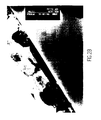
- the aluminum texture and morphology was assessed visually from photomicrographs taken of cross-sections of the stack, such as shown in FIG. 2A (silane oxide, i.e., plasma silane), where the Al 3 Ti layer has a sightly undulated, yet smooth surface as can be seen, and FIG. 2B (HDP oxide), where the Al 3 Ti layer has a very smooth surface contour.
- the oxide layer is the bulk layer occupying the lower right-hand corner.
- enhanced aluminum alloy film texture is accompanied by reduced film resistivity, better film planarity, and a smoother TiAl 3 morphology (larger process window) useful in preventing agglomeration of the hot aluminum stack, as shown in Figures 2A and 2B for the examples of silane oxide and high density plasma (HDP) oxide, respectively.
- Table 2 also indicates that film reflectivity is a quick and useful in-line measurement technique for these benefits.
- Table 3 shows the reflectivities and resistivities of hot aluminum films deposited on silane oxide and plasma TEOS oxide layers as surface treated (i.e., planarized) by chemical-mechanical polishing (CMP) and two oxide etch processes.
- CMP chemical-mechanical polishing
- silane oxide samples 1-4 6450 ⁇ of silane oxide was formed for each sample under the same conditions described in Table 1 for forming "Silane Oxide" in a LPCVD system.
- TEOS samples 1-4 a 6450 ⁇ thick silicon oxide layer was formed for each sample by pyrolytic oxidation of tetraethylorthosilane (TEOS) in a PECVD system under the same conditions described for forming "Plasma TEOS" in Table 1.
- TEOS tetraethylorthosilane
- the oxide films, after formation and before metal deposition thereon, were either etched according to etch condition M1 or C1, or chemical-mechanical planarized, to remove 1000 to 1500 ⁇ of surface oxide.
- etch condition M1 used to planarize Silane Oxide 1 and Plasma TEOS Oxide 1 the oxide layer was dry etched in a plasma reactor with a plasma formed from 20 SCCM CHF 3 , 60 SCCM CF 4 , 500 SCCM Argon and 10 Torr helium for 15 seconds at 240 mTorr, 1300 W, with an upper electrode at 40°C and lower electrode at 15°C and spacing of 1 cm.
- etch condition C1 used to planarize Silane Oxide 2 and Plasma TEOS Oxide 2 the oxide layer was dry etched in a plasma formed in a reactive ion etcher from 10 SCCM C 4 F 8 , 50 SCCM CO, and 200 SCCM Argon for 25 seconds at 40 mTorr, 2000 W, with a 60°C wall and 0°C wafer and a spacing of 30 cm.
- the CMP was carried out with fused silica base slurry and the down force was 7.5 psi.
- metal lines were formed on each type of oxide studied.
- the metal lines were formed in the same manner on each oxide substrate by sequential sputter-deposition of a 200 ⁇ titanium layer; then a 2000 ⁇ AlCuSi alloy (50°C), and finally a 5500 ⁇ AlCu (525°C) layer, in that sequence, using a multichamber dc-magnetron sputtering system having a base pressure of about 2 x 10 -8 Torr.
- the metal lines patterns were formed by conventional photolithographic methods.
- the insulator/metal film structures were annealed at 400°C in flowing N 2 (90%)/H 2 (10%) ambient for 20 minutes.
- TEOS derived-oxides silane oxides, high density plasma oxides
- oxide forming techniques can be utilised, such as thermally grown oxide.
- other insulator substrate materials, and not merely oxides, that can be imbued with smooth surfaces can also be used as the underlayer for the aluminum films to yield similar results in favorably controlling the aluminum texture for elctromigration performance and metal line reliability in an aluminum (alloy) layered interconnection.
Landscapes
- Internal Circuitry In Semiconductor Integrated Circuit Devices (AREA)
Applications Claiming Priority (2)
| Application Number | Priority Date | Filing Date | Title |
|---|---|---|---|
| US661160 | 1996-06-10 | ||
| US08/661,160 US6200894B1 (en) | 1996-06-10 | 1996-06-10 | Method for enhancing aluminum interconnect properties |
Publications (2)
| Publication Number | Publication Date |
|---|---|
| EP0813245A2 true EP0813245A2 (de) | 1997-12-17 |
| EP0813245A3 EP0813245A3 (de) | 2000-01-05 |
Family
ID=24652458
Family Applications (1)
| Application Number | Title | Priority Date | Filing Date |
|---|---|---|---|
| EP97303858A Withdrawn EP0813245A3 (de) | 1996-06-10 | 1997-06-05 | Aluminium-Zwischenverbindungen |
Country Status (3)
| Country | Link |
|---|---|
| US (1) | US6200894B1 (de) |
| EP (1) | EP0813245A3 (de) |
| JP (1) | JPH1056011A (de) |
Cited By (1)
| Publication number | Priority date | Publication date | Assignee | Title |
|---|---|---|---|---|
| US5928967A (en) * | 1996-06-10 | 1999-07-27 | International Business Machines Corporation | Selective oxide-to-nitride etch process using C4 F8 /CO/Ar |
Families Citing this family (7)
| Publication number | Priority date | Publication date | Assignee | Title |
|---|---|---|---|---|
| SE513809C2 (sv) * | 1999-04-13 | 2000-11-06 | Ericsson Telefon Ab L M | Avstämbara mikrovågsanordningar |
| KR100399066B1 (ko) * | 2000-12-28 | 2003-09-26 | 주식회사 하이닉스반도체 | 반도체소자의 알루미늄 합금 박막 제조 방법 |
| JP2007053133A (ja) * | 2005-08-15 | 2007-03-01 | Toshiba Corp | 半導体装置及びその製造方法 |
| KR100732861B1 (ko) | 2005-12-27 | 2007-06-27 | 동부일렉트로닉스 주식회사 | 반도체 배선 및 그 형성 방법 |
| US20080135827A1 (en) * | 2006-09-25 | 2008-06-12 | Stmicroelectronics Crolles 2 Sas | MIM transistor |
| WO2009055156A1 (en) * | 2007-10-26 | 2009-04-30 | Hvvi Semiconductors, Inc. | Semiconductor structure and method of manufacture |
| CN120225576A (zh) | 2022-12-27 | 2025-06-27 | 电化株式会社 | 共聚物、其制造方法及包含共聚物的固化体 |
Family Cites Families (10)
| Publication number | Priority date | Publication date | Assignee | Title |
|---|---|---|---|---|
| US4017890A (en) | 1975-10-24 | 1977-04-12 | International Business Machines Corporation | Intermetallic compound layer in thin films for improved electromigration resistance |
| US4438450A (en) | 1979-11-30 | 1984-03-20 | Bell Telephone Laboratories, Incorporated | Solid state device with conductors having chain-shaped grain structure |
| US4352239A (en) | 1980-04-17 | 1982-10-05 | Fairchild Camera And Instrument | Process for suppressing electromigration in conducting lines formed on integrated circuits by control of crystalline boundary orientation |
| DE3164742D1 (en) * | 1980-09-22 | 1984-08-16 | Tokyo Shibaura Electric Co | Method of smoothing an insulating layer formed on a semiconductor body |
| US4922320A (en) | 1985-03-11 | 1990-05-01 | Texas Instruments Incorporated | Integrated circuit metallization with reduced electromigration |
| US5001541A (en) | 1989-03-22 | 1991-03-19 | Texas Instruments Incorporated | Advanced electromigration resistant interconnect structure and process |
| US5240880A (en) | 1992-05-05 | 1993-08-31 | Zilog, Inc. | Ti/TiN/Ti contact metallization |
| US5360995A (en) | 1993-09-14 | 1994-11-01 | Texas Instruments Incorporated | Buffered capped interconnect for a semiconductor device |
| US5851602A (en) * | 1993-12-09 | 1998-12-22 | Applied Materials, Inc. | Deposition of high quality conformal silicon oxide thin films for the manufacture of thin film transistors |
| US5494854A (en) * | 1994-08-17 | 1996-02-27 | Texas Instruments Incorporated | Enhancement in throughput and planarity during CMP using a dielectric stack containing HDP-SiO2 films |
-
1996
- 1996-06-10 US US08/661,160 patent/US6200894B1/en not_active Expired - Fee Related
-
1997
- 1997-06-04 JP JP9146805A patent/JPH1056011A/ja active Pending
- 1997-06-05 EP EP97303858A patent/EP0813245A3/de not_active Withdrawn
Non-Patent Citations (2)
| Title |
|---|
| ONODA H E.A.: "Effects of insulator surface roughness on Al-alloy film crystallographic orientation in Al-alloy/Ti/insulator structure" JAPANESE JOURNAL OF APPLIED PHYSICS PART 2 LETTERS,15 August 1995, pages l1037-l1040, XP002110474 Japan * |
| RODBELL K P E.A.: "Film crystallographic texture and substrate surface roughness in layered aluminium metallization" MATERIALS RELIABILITY IN MICROELECTRONICS VI. SYMPOSIUM, SAN FRANCISCO, CA, USA, 8-12 APRIL 1996, MATER. RES. SOC, PITTSBURGH, USA, XP002110475 * |
Cited By (1)
| Publication number | Priority date | Publication date | Assignee | Title |
|---|---|---|---|---|
| US5928967A (en) * | 1996-06-10 | 1999-07-27 | International Business Machines Corporation | Selective oxide-to-nitride etch process using C4 F8 /CO/Ar |
Also Published As
| Publication number | Publication date |
|---|---|
| US6200894B1 (en) | 2001-03-13 |
| EP0813245A3 (de) | 2000-01-05 |
| JPH1056011A (ja) | 1998-02-24 |
Similar Documents
| Publication | Publication Date | Title |
|---|---|---|
| EP0721216B1 (de) | Weicher Metallleiter und Herstellungsverfahren | |
| US6261951B1 (en) | Plasma treatment to enhance inorganic dielectric adhesion to copper | |
| US6391777B1 (en) | Two-stage Cu anneal to improve Cu damascene process | |
| US6436825B1 (en) | Method of copper barrier layer formation | |
| US6554914B1 (en) | Passivation of copper in dual damascene metalization | |
| US6255733B1 (en) | Metal-alloy interconnections for integrated circuits | |
| US6465376B2 (en) | Method and structure for improving electromigration of chip interconnects | |
| EP0552968A2 (de) | Halbleiteranordnung mit einer Leiterschicht | |
| JPH077077A (ja) | 半導体装置及びその製造方法 | |
| US6306761B1 (en) | Method of manufacturing semiconductor device | |
| JPH0752733B2 (ja) | 配線構造体の形成方法 | |
| JPH1041247A (ja) | 自己調心超薄膜を用いたcvdアルミニウムのブランケット選択的堆積及び反射率の改善 | |
| JPH0653163A (ja) | 集積回路障壁構造体とその製法 | |
| US5747879A (en) | Interface between titanium and aluminum-alloy in metal stack for integrated circuit | |
| JP2951636B2 (ja) | メタライゼーション構造を製造する方法 | |
| JP4949551B2 (ja) | 銅相互接続の電気移動耐性が改善されるように調整されたバリヤー層 | |
| KR100331906B1 (ko) | 반도체 장치의 제조 방법 | |
| US6077782A (en) | Method to improve the texture of aluminum metallization | |
| EP0813245A2 (de) | Aluminium-Zwischenverbindungen | |
| US6468908B1 (en) | Al-Cu alloy sputtering method with post-metal quench | |
| US20030008494A1 (en) | Multi-step planarizing method for forming a patterned thermally extrudable material layer | |
| US6876082B2 (en) | Refractory metal nitride barrier layer with gradient nitrogen concentration | |
| US6448172B1 (en) | Manufacturing method of forming interconnection in semiconductor device | |
| US6045892A (en) | Metal wiring structures for integrated circuits including seed layer | |
| JPH11511593A (ja) | 専用チャンバによる2層のチタン薄層を有する集積回路用金属スタック |
Legal Events
| Date | Code | Title | Description |
|---|---|---|---|
| PUAI | Public reference made under article 153(3) epc to a published international application that has entered the european phase |
Free format text: ORIGINAL CODE: 0009012 |
|
| AK | Designated contracting states |
Kind code of ref document: A2 Designated state(s): DE FR GB |
|
| PUAL | Search report despatched |
Free format text: ORIGINAL CODE: 0009013 |
|
| AK | Designated contracting states |
Kind code of ref document: A3 Designated state(s): AT BE CH DE DK ES FI FR GB GR IE IT LI LU MC NL PT SE |
|
| AKX | Designation fees paid |
Free format text: DE FR GB |
|
| STAA | Information on the status of an ep patent application or granted ep patent |
Free format text: STATUS: THE APPLICATION IS DEEMED TO BE WITHDRAWN |
|
| 18D | Application deemed to be withdrawn |
Effective date: 20000706 |