EP0816892A2 - Katadioptrisches Linsensystem - Google Patents
Katadioptrisches Linsensystem Download PDFInfo
- Publication number
- EP0816892A2 EP0816892A2 EP97110124A EP97110124A EP0816892A2 EP 0816892 A2 EP0816892 A2 EP 0816892A2 EP 97110124 A EP97110124 A EP 97110124A EP 97110124 A EP97110124 A EP 97110124A EP 0816892 A2 EP0816892 A2 EP 0816892A2
- Authority
- EP
- European Patent Office
- Prior art keywords
- lens system
- lens
- catadioptric
- refractive
- reticle
- Prior art date
- Legal status (The legal status is an assumption and is not a legal conclusion. Google has not performed a legal analysis and makes no representation as to the accuracy of the status listed.)
- Withdrawn
Links
Images


Classifications
-
- G—PHYSICS
- G02—OPTICS
- G02B—OPTICAL ELEMENTS, SYSTEMS OR APPARATUS
- G02B17/00—Systems with reflecting surfaces, with or without refracting elements
- G02B17/08—Catadioptric systems
- G02B17/0892—Catadioptric systems specially adapted for the UV
-
- G—PHYSICS
- G02—OPTICS
- G02B—OPTICAL ELEMENTS, SYSTEMS OR APPARATUS
- G02B17/00—Systems with reflecting surfaces, with or without refracting elements
- G02B17/08—Catadioptric systems
-
- G—PHYSICS
- G03—PHOTOGRAPHY; CINEMATOGRAPHY; ANALOGOUS TECHNIQUES USING WAVES OTHER THAN OPTICAL WAVES; ELECTROGRAPHY; HOLOGRAPHY
- G03F—PHOTOMECHANICAL PRODUCTION OF TEXTURED OR PATTERNED SURFACES, e.g. FOR PRINTING, FOR PROCESSING OF SEMICONDUCTOR DEVICES; MATERIALS THEREFOR; ORIGINALS THEREFOR; APPARATUS SPECIALLY ADAPTED THEREFOR
- G03F7/00—Photomechanical, e.g. photolithographic, production of textured or patterned surfaces, e.g. printing surfaces; Materials therefor, e.g. comprising photoresists; Apparatus specially adapted therefor
- G03F7/20—Exposure; Apparatus therefor
- G03F7/2002—Exposure; Apparatus therefor with visible light or UV light, through an original having an opaque pattern on a transparent support, e.g. film printing, projection printing; by reflection of visible or UV light from an original such as a printed image
-
- G—PHYSICS
- G03—PHOTOGRAPHY; CINEMATOGRAPHY; ANALOGOUS TECHNIQUES USING WAVES OTHER THAN OPTICAL WAVES; ELECTROGRAPHY; HOLOGRAPHY
- G03F—PHOTOMECHANICAL PRODUCTION OF TEXTURED OR PATTERNED SURFACES, e.g. FOR PRINTING, FOR PROCESSING OF SEMICONDUCTOR DEVICES; MATERIALS THEREFOR; ORIGINALS THEREFOR; APPARATUS SPECIALLY ADAPTED THEREFOR
- G03F7/00—Photomechanical, e.g. photolithographic, production of textured or patterned surfaces, e.g. printing surfaces; Materials therefor, e.g. comprising photoresists; Apparatus specially adapted therefor
- G03F7/70—Microphotolithographic exposure; Apparatus therefor
- G03F7/70216—Mask projection systems
- G03F7/70225—Optical aspects of catadioptric systems, i.e. comprising reflective and refractive elements
-
- G—PHYSICS
- G03—PHOTOGRAPHY; CINEMATOGRAPHY; ANALOGOUS TECHNIQUES USING WAVES OTHER THAN OPTICAL WAVES; ELECTROGRAPHY; HOLOGRAPHY
- G03F—PHOTOMECHANICAL PRODUCTION OF TEXTURED OR PATTERNED SURFACES, e.g. FOR PRINTING, FOR PROCESSING OF SEMICONDUCTOR DEVICES; MATERIALS THEREFOR; ORIGINALS THEREFOR; APPARATUS SPECIALLY ADAPTED THEREFOR
- G03F7/00—Photomechanical, e.g. photolithographic, production of textured or patterned surfaces, e.g. printing surfaces; Materials therefor, e.g. comprising photoresists; Apparatus specially adapted therefor
- G03F7/70—Microphotolithographic exposure; Apparatus therefor
- G03F7/70216—Mask projection systems
- G03F7/7025—Size or form of projection system aperture, e.g. aperture stops, diaphragms or pupil obscuration; Control thereof
Definitions
- the present invention relates to the lens system in a projection exposure apparatus used for manufacturing semiconductor devices or liquid crystal devices and the like via photolithographic processing.
- the invention specifically relates to a catadioptric lens system which is capable of providing a photolithographic resolution of quarter micron levels in the ultraviolet band region by using a reflective mirror as an element of the lens system.
- a projection exposure apparatus In photolithographic processing for manufacturing semiconductor devices and the like, a projection exposure apparatus is used in which a semiconductor device pattern printed onto a photomask or reticle (hereafter both are referred to as reticle) is exposed via a projection lens system onto a substrate such as a wafer or glass plate (hereafter both are referred to as a wafer) coated with photoresist and the like.
- reticle a semiconductor device pattern printed onto a photomask or reticle
- a substrate such as a wafer or glass plate
- NA numerical aperture
- Various technologies have been proposed in order to meet the requirement in which a projection lens system is constructed with a so called "catadioptric lens system" which is a combination of a reflective system and a refractive system.
- Japanese patent kokai S63-163319 and kokai H5-25170 disclose a catadioptric lens system which uses an exposure region including light on the optical axis.
- kokai H7-111512 and US 4,779,966 use light on the exposure region of a ring field, rather than light on the optical axis.
- a beam splitter having a transmittive reflective surface is required for splitting the optical path.
- This lens system may easily generate light aberrations, causing flares or uneven illumination on the surface of a wafer. These light aberrations are generated from internal reflections from the wafer surface, from a refractive surface of the lens systems arranged behind the beam splitter, or from the transmittive reflective surface of a beam splitter and the like.
- a lens system with a larger numerical aperture requires a larger beam splitter and a longer exposure time due to the decrease in light intensity. This in turn, causes a decrease in throughput of the semiconductor manufacturing process.
- a reflection beam splitter is required to prevent loss of light intensity, however, it is very difficult to manufacture a large reflection beam splitter and its use gives unfavorable imaging performance due to the uneven film thickness of the transmittive reflective layer, which affects the deflection, absorption, and phase change of the light, etc.
- the first lens system including a concave mirror for forming an interim image is constructed with a lens system in perfect symmetry, and the size of the interim image remains the same as the real size of the reticle surface.
- the possibility of generating aberrations in the first imaging lens is reduced, however, this gives a heavier load onto the second imaging lens system.
- a large NA is required for the lens system, it is inevitable that the size and complexity of the second lens systemmust be increased.
- the present invention intends to resolve the problem by providing a catadioptric lens system whose entire size is essentially compact and is capable of providing a large numerical aperture in the ultraviolet band region to obtain the photolithographic resolution of quarter micron levels and is constructed with components of reduced sizes.
- the present invention provides a catadioptric lens system characterized by the fact that the catadioptric lens system comprises:
- the invention further relates to a catadioptric lens system comprising:
- the catadioptric lens system of the present invention is further characterized by a) a first lens system constructed with refractive members, b) a concave mirror, and c) a second lens system constructed with refractive members to project a semiconductor device pattern from a reticle surface onto a substrate wherein the first lens system comprises:
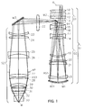
- Figure 1 shows a layout of a catadioptric lens system of embodiment 1.
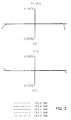
- Figure 2 shows an aberration diagram of a catadioptric lens system of embodiment 1.
- Figure 3 shows a layout of a catadioptric lens system of embodiment 2.
- Figure 4 shows an aberration diagram of a catadioptric lens system of embodiment 2.
- the chance of generating aberrations of high orders is reduced and the NA of the lens system is increased, thus preventing an increase in the complexity and size of the lens system.
- Changing the refractive surface from a spherical surface ideally bends light flux which exists around the lens surface. This makes it possible to correct aberrations of high orders without broadening the entire flux.
- Introducing aspherical refractive surfaces to the first lens system S1 prevents increasing the size of it.
- Introducing aspherical refractive surfaces to the second lens system S2 also prevents increasing the size of it.
- the first lens system S1 comprises a first lens group G1, in which light enters only once and a second lens group G2 in which light makes a round trip.
- the lens closest to the concave mirror M1 of the second lens group G2 is a negative lens LS.
- Light coming through the second lens group G2 images a semiconductor device pattern once before entering the second lens system S2. This configuration of the lens system especially allows decreasing the size of each of its component members.
- the configuration is very effective in reducing chromatic aberration on the axis wherein the configuration includes, in order in which light progresses, a negative lens LS which is closest to the concave mirror M1 in the second lens group G2, a concave mirror M1, and the second lens system S2 wherein the semiconductor device pattern is imaged once before light emitted from the second lens group G2 enters the second lens system S2.
- the second lens group G2 is constructed with a refractive member having at least two different negative refractive powers and a refractive member having at least two different positive refractive powers.
- the lens having negative refractive powers is effective in correcting coma or spherical aberrations and image curvature and the like.
- the lens having positive refractive powers is effective in not increasing the size of the lens system and provides a large NA or exposure region.
- each of the members have at least two lenses in order to reduce the load for correcting aberrations of the second lens systemS2.
- the first lens group G1 is constructed with refractive members having three different refractive powers. Lately, as the demand for higher resolution increases, more stringent specifications are demanded for correcting distortion, image curvature and the like. It is important for one to adjust these parameters during manufacturing to meet this demand. These adjustments for a lens positioned in the vicinity of the reticle surface work effectively.
- the second lens group G2 of the present invention is the lens system for both outgoing and incoming light, which is inappropriate for adjustment lenses. For this reason, constructing the first lens group G1 with lenses having at least three different refractive powers makes it possible to adjust distortion or curvature aberration during manufacturing of lens systems. Also, by utilizing the first lens group G1 in the aforementioned configuration, the working distance in the vicinity of the surface of the reticle R can be increased and a step and scan method of exposure is made possible.
- the second lens system S2 plays an important role in correcting mainly spherical or coma aberrations to allow the lens system to have a large NA.
- a second optical path reflection member M3 between the first lens system S1 and the second lens system S2 or in the second lens system S2. Also, it is possible to dispose the reflection member M3 in the second imaging lens system. By installing an optical path reflection member such as a mirror, the entire lens system can be bent, reducing its entire size.
- quartz or fluorite are preferable as the material for a refraction member. These minerals are excellent in illumination transmissivity, they are inexpensive, and they are easy to process.
- the concave mirror M1 can be formed aspherically. If a concave minor M1 is aspherical, the magnitude of the positive refractive power of the concave mirror M1 can be increased without generating aberrations of high orders which makes it possible to manufacture compact lens systems having a large NA and also allows correcting chromatic aberration over a wide bandwidth.
- the coherence factor ( ⁇ value) can be adjusted.
- a technique to increase focal depth and improve resolution is disclosed for example in Japanese patent kokai S62-50811 in which a phase shift technique is used to shift the phase of a predetermined portion of the reticle pattern from another portion.
- the present invention provides increased effect of the phase shift technique with adjustment of the coherence factor ( ⁇ value).
- the catadioptric lens system in each of the quantitative embodiments comprises, in order from the reticle R side (in the order that light progresses):
- NA 0.6 in each of the quantitative embodiments, and aberrations for the image height are corrected within the range of about 5 to about 18.6.
- the range for the aforementioned image height may be a ring field or may be a rectangle of 6 x 30 at a distance of 5 from the optical axis.
- r denotes surface curvature radius and d denotes a distance between surfaces.
- Glassy materials are denoted as SiO 2 for quartz and CaF 2 for fluorite in each of the tables.
- the refraction rates for quartz and fluorite for n, at 193.0 nm, and for 1/v, which is the dispersion value for those of ⁇ 0.1nm, are as follows: n 1 /v synthetic quartz: 1.56019 1780 fluorite 1.50138 2550
- an aspherical surface is shown by the following equation where:
- a first lens group G1 comprises, in order from the side of the surface of the reticle R, a biconvex lens 10, a biconcave lens 11, a meniscus lens 12 whose convexity points to the side of the surface of the reticle R, and parallel plane plates 13.
- the second lens group comprises, in order from the surface of the reticle R, a biconvex lens 14, a biconcave lens 15, a biconvex lens 16, a biconcave lens 17, a biconvex lens 18, a meniscus lens 19 whose concavity points to the side of the surface of the reticle R, a biconvex lens 20, a meniscus lens 21 whose convexity points to the side of the surface of the reticle R, and a negative meniscus lens LS whose concavity points to the surface of the reticle R and is formed with an aspherical surface AS1 on the side of the reticle R.
- Parallel plane plates 13 in the first lens group G1 comprise a plane mirror M2 which is made by polishing a part of the lens to function as a first optical path reflection member M2.
- the image of the reticle R is formed once in the vicinity of the plane mirror M2.
- the concave minor M1 is formed on an aspherical surface AS2.
- the second lens system S2 comprises, in order from the surface of the reticle R, a biconvex lens 22 (which can be arranged in the second lens system S2 or can be arranged between the first and second lens systems S1and S2 respectively), a meniscus lens 23 whose concavity points to the side of the surface of the reticle R, a biconvex lens 24, a meniscus lens 25 whose convexity points to the side of the surface of the reticle R, a biconvex lens 26, an aperture stop AP, a bioconvex lens 27, a meniscus lens 28 formed with an aspherical surface AS3 whose convexity points to the surface of the reticle R, a meniscus lens 29 whose convexity points to the side of the surface of the reticle R, a meniscus lens 30 whose convexity points to the side of the surface of the reticle R, a biconcave lens 31, a meniscus lens 32 whose concavity points to the side of the
- a plane mirror M3 is arranged optically between the first lens 22 and the second lens 23 of the second lens system S2 or in the second lens system S2 such that surfaces of a reticle R and a wafer W are arranged in parallel.
- the required parameters comprise a NA of 0.6, the image height Y of 18.6, and the diameter of about 20 for all optical members of the catadioptric lens system.
- a first lens group G1 of the first lens system comprises, in order from the surface of the reticle R, a meniscus lens 34 whose convexity points to the side of the surface of the reticle R, a biconvex lens 35, a biconcave lens 36, a meniscus lens 37 whose convexity points to the side of the surface of the reticle R, and parallel plane plate 38.
- the second lens group G2 of the first lens system comprises, in order from the surface of the reticle R, a biconvex lens 39, a meniscus lens 40 whose concavity points to the side of the surface of the reticle, a biconvex lens 41, a meniscus lens 42 whose convexity points to the side of the surface of the reticle R, biconcave lens 43, biconvex lens 44, a meniscus lens 45 whose convexity points to the side of the surface of the reticle R, a biconvex lens 46, a meniscus lens 47 whose concavity points to the side of the surface of the reticle R, and a negative meniscus lens LS whose concavity points to the surface of the reticle R.
- Parallel plane plates in the first lens group G1 comprises a plane mirror M2 which is made by polishing a surface of the lens to function as an optical reflection member.
- the image of the reticle R is formed once in the vicinity of the plane mirror M2.
- the concave mirror M1 is formed on an aspherical surface AS2.
- the second lens system S2 comprises, in order from the surface of the reticle R, a biconvex lens 48, a meniscus lens 49 whose convexity points to the side of the surface of the reticle R, (the biconvex lens 48 and the meniscus lens 49 may be arranged within the second lens system S2 or between the first and second lens systems S1 and S2 respectively), meniscus lens 50 whose convexity points to the side of the surface of the reticle R, a meniscus lens 51 whose concavity points to the side of the surface of the reticle R, an aperture stop P, a biconvex lens 52 whose surface on the side of the reticle R is formed with an aspherical surface AS2, a meniscus lens 53 whose convexity points to the side of the surface of the reticle R, a biconcave lens 54, a meniscus lens 55 whose convexity points to the side of the surface of the reticle R, a meniscus lens 56 whose convevex
- the required parameters comprise a NA of 0.6, an image height Y of 18.6, and a diameter of about 20 for all optical members of the catadioptric lens system.
- the present invention can provide a catadioptric lens system whose entire size is practically compact and is capable of providing a large numerical aperture in the ultraviolet band.
- the invention also provides photolithographic resolution of quarter micron levels and is easy to manufacture.
Landscapes
- Physics & Mathematics (AREA)
- General Physics & Mathematics (AREA)
- Optics & Photonics (AREA)
- Lenses (AREA)
- Exposure Of Semiconductors, Excluding Electron Or Ion Beam Exposure (AREA)
- Exposure And Positioning Against Photoresist Photosensitive Materials (AREA)
Applications Claiming Priority (3)
| Application Number | Priority Date | Filing Date | Title |
|---|---|---|---|
| JP8153770A JPH103039A (ja) | 1996-06-14 | 1996-06-14 | 反射屈折光学系 |
| JP153770/96 | 1996-06-14 | ||
| JP15377096 | 1996-06-14 |
Publications (2)
| Publication Number | Publication Date |
|---|---|
| EP0816892A2 true EP0816892A2 (de) | 1998-01-07 |
| EP0816892A3 EP0816892A3 (de) | 1999-06-09 |
Family
ID=15569767
Family Applications (1)
| Application Number | Title | Priority Date | Filing Date |
|---|---|---|---|
| EP97110124A Withdrawn EP0816892A3 (de) | 1996-06-14 | 1997-06-16 | Katadioptrisches Linsensystem |
Country Status (3)
| Country | Link |
|---|---|
| EP (1) | EP0816892A3 (de) |
| JP (1) | JPH103039A (de) |
| KR (1) | KR980005325A (de) |
Cited By (22)
| Publication number | Priority date | Publication date | Assignee | Title |
|---|---|---|---|---|
| EP0869383A3 (de) * | 1997-04-01 | 1999-09-08 | Nikon Corporation | Katadioptrisches optisches System |
| US6195213B1 (en) | 1998-06-08 | 2001-02-27 | Nikon Corporation | Projection exposure apparatus and method |
| WO2001050171A1 (de) * | 1999-12-29 | 2001-07-12 | Carl Zeiss | Projektionsobjektiv mit benachbart angeordneten asphärischen linsenoberflächen |
| EP1094350A3 (de) * | 1999-10-21 | 2001-08-16 | Carl Zeiss | Optisches Projektionslinsensystem |
| EP0989434A3 (de) * | 1998-07-29 | 2001-10-17 | Carl Zeiss | Catadioptrisches System und dieses verwendender Belichtungsapparat |
| US6366342B2 (en) | 2000-03-21 | 2002-04-02 | Nikon Corporation | Drive apparatus, exposure apparatus, and method of using the same |
| US6377338B1 (en) | 1998-08-18 | 2002-04-23 | Nikon Corporation | Exposure apparatus and method |
| US6509957B1 (en) | 1999-12-01 | 2003-01-21 | Nikon Corporation | Stage device and exposure apparatus |
| US6636350B2 (en) | 2000-01-14 | 2003-10-21 | Carl-Zeiss-Stiftung | Microlithographic reduction projection catadioptric objective |
| US6654100B2 (en) | 2000-03-09 | 2003-11-25 | Nikon Corporation | Stage device and exposure apparatus, and method of manufacturing a device |
| US6707616B1 (en) | 1998-04-07 | 2004-03-16 | Nikon Corporation | Projection exposure apparatus, projection exposure method and catadioptric optical system |
| US6985210B2 (en) | 1999-02-15 | 2006-01-10 | Carl Zeiss Smt Ag | Projection system for EUV lithography |
| US6995833B2 (en) | 2003-05-23 | 2006-02-07 | Canon Kabushiki Kaisha | Projection optical system, exposure apparatus, and device manufacturing method |
| US7151592B2 (en) | 1999-02-15 | 2006-12-19 | Carl Zeiss Smt Ag | Projection system for EUV lithography |
| US7190527B2 (en) | 2002-03-01 | 2007-03-13 | Carl Zeiss Smt Ag | Refractive projection objective |
| US7237915B2 (en) | 2000-01-14 | 2007-07-03 | Carl Zeiss Smt Ag | Catadioptric projection system for 157 nm lithography |
| US7339743B2 (en) | 2002-03-01 | 2008-03-04 | Carl Zeiss Smt Ag | Very-high aperture projection objective |
| US7830046B2 (en) | 2007-03-16 | 2010-11-09 | Nikon Corporation | Damper for a stage assembly |
| USRE42118E1 (en) * | 1999-02-15 | 2011-02-08 | Carl-Zeiss-Smt Ag | Projection system for EUV lithography |
| US8908269B2 (en) | 2004-01-14 | 2014-12-09 | Carl Zeiss Smt Gmbh | Immersion catadioptric projection objective having two intermediate images |
| US9726979B2 (en) | 2004-05-17 | 2017-08-08 | Carl Zeiss Smt Gmbh | Catadioptric projection objective with intermediate images |
| US9772478B2 (en) | 2004-01-14 | 2017-09-26 | Carl Zeiss Smt Gmbh | Catadioptric projection objective with parallel, offset optical axes |
Families Citing this family (25)
| Publication number | Priority date | Publication date | Assignee | Title |
|---|---|---|---|---|
| US20030155882A1 (en) | 2002-02-19 | 2003-08-21 | Nikon Corporation | Anti-gravity mount with air and magnets |
| SG2010050110A (en) | 2002-11-12 | 2014-06-27 | Asml Netherlands Bv | Lithographic apparatus and device manufacturing method |
| KR20170018113A (ko) | 2003-04-09 | 2017-02-15 | 가부시키가이샤 니콘 | 노광 방법 및 장치, 그리고 디바이스 제조 방법 |
| KR20180089562A (ko) | 2003-04-10 | 2018-08-08 | 가부시키가이샤 니콘 | 액침 리소그래피 장치용 진공 배출을 포함하는 환경 시스템 |
| EP3062152B1 (de) | 2003-04-10 | 2017-12-20 | Nikon Corporation | Umgebungssystem mit einer transportregion für eine immersionslithografievorrichtung |
| JP4315198B2 (ja) | 2003-04-11 | 2009-08-19 | 株式会社ニコン | 液浸液体を光学アセンブリ下に維持するリソグラフィ装置及び液浸液体維持方法並びにそれらを用いるデバイス製造方法 |
| TWI295414B (en) | 2003-05-13 | 2008-04-01 | Asml Netherlands Bv | Lithographic apparatus and device manufacturing method |
| DE602004024782D1 (de) | 2003-06-19 | 2010-02-04 | Nippon Kogaku Kk | Belichtungseinrichtung und bauelementeherstellungsverfahren |
| EP3179309A1 (de) | 2003-07-08 | 2017-06-14 | Nikon Corporation | Waferplatte für die immersionslithografie |
| TWI569308B (zh) | 2003-10-28 | 2017-02-01 | 尼康股份有限公司 | 照明光學裝置、曝光裝置、曝光方法以及元件製造 方法 |
| TWI512335B (zh) | 2003-11-20 | 2015-12-11 | 尼康股份有限公司 | 光束變換元件、光學照明裝置、曝光裝置、以及曝光方法 |
| US7589822B2 (en) | 2004-02-02 | 2009-09-15 | Nikon Corporation | Stage drive method and stage unit, exposure apparatus, and device manufacturing method |
| TWI505329B (zh) | 2004-02-06 | 2015-10-21 | 尼康股份有限公司 | 光學照明裝置、曝光裝置、曝光方法以及元件製造方法 |
| KR101504445B1 (ko) | 2004-03-25 | 2015-03-19 | 가부시키가이샤 니콘 | 노광 장치 및 디바이스 제조 방법 |
| US7324185B2 (en) | 2005-03-04 | 2008-01-29 | Asml Netherlands B.V. | Lithographic apparatus and device manufacturing method |
| US8248577B2 (en) | 2005-05-03 | 2012-08-21 | Asml Netherlands B.V. | Lithographic apparatus and device manufacturing method |
| KR101544336B1 (ko) | 2005-05-12 | 2015-08-12 | 가부시키가이샤 니콘 | 투영 광학계, 노광 장치 및 노광 방법 |
| US20080073563A1 (en) | 2006-07-01 | 2008-03-27 | Nikon Corporation | Exposure apparatus that includes a phase change circulation system for movers |
| JP5267029B2 (ja) | 2007-10-12 | 2013-08-21 | 株式会社ニコン | 照明光学装置、露光装置及びデバイスの製造方法 |
| US8379187B2 (en) | 2007-10-24 | 2013-02-19 | Nikon Corporation | Optical unit, illumination optical apparatus, exposure apparatus, and device manufacturing method |
| US9116346B2 (en) | 2007-11-06 | 2015-08-25 | Nikon Corporation | Illumination apparatus, illumination method, exposure apparatus, and device manufacturing method |
| EP2381310B1 (de) | 2010-04-22 | 2015-05-06 | ASML Netherlands BV | Flüssigkeitshandhabungsstruktur und lithographischer Apparat |
| US20130255414A1 (en) | 2010-09-09 | 2013-10-03 | Nikon Corporation | Parallel Linkage and Actuator Motor Coil Designs for Tube Carrier |
| US8572518B2 (en) | 2011-06-23 | 2013-10-29 | Nikon Precision Inc. | Predicting pattern critical dimensions in a lithographic exposure process |
| US9030057B2 (en) | 2011-06-24 | 2015-05-12 | Nikon Corporation | Method and apparatus to allow a plurality of stages to operate in close proximity |
Family Cites Families (6)
| Publication number | Priority date | Publication date | Assignee | Title |
|---|---|---|---|---|
| US5140459A (en) * | 1989-08-29 | 1992-08-18 | Texas Instruments | Apparatus and method for optical relay and reimaging |
| JPH04367213A (ja) * | 1991-06-13 | 1992-12-18 | Orc Mfg Co Ltd | 投影型露光装置 |
| EP0527043B1 (de) * | 1991-08-05 | 1997-01-22 | Nikon Corporation | Verkleinerndes katadioptrisches Projektionssystem |
| US5212593A (en) * | 1992-02-06 | 1993-05-18 | Svg Lithography Systems, Inc. | Broad band optical reduction system using matched multiple refractive element materials |
| EP0604093B1 (de) * | 1992-12-24 | 1997-11-19 | Nikon Corporation | Verkleinerndes katadioptrisches Projektionssystem |
| US5537260A (en) * | 1993-01-26 | 1996-07-16 | Svg Lithography Systems, Inc. | Catadioptric optical reduction system with high numerical aperture |
-
1996
- 1996-06-14 JP JP8153770A patent/JPH103039A/ja active Pending
-
1997
- 1997-05-28 KR KR1019970021291A patent/KR980005325A/ko not_active Withdrawn
- 1997-06-16 EP EP97110124A patent/EP0816892A3/de not_active Withdrawn
Cited By (43)
| Publication number | Priority date | Publication date | Assignee | Title |
|---|---|---|---|---|
| EP0869383A3 (de) * | 1997-04-01 | 1999-09-08 | Nikon Corporation | Katadioptrisches optisches System |
| EP1079253A4 (de) * | 1998-04-07 | 2004-09-01 | Nikon Corp | Vorrichtung und verfahren zur projektionsbelichtung, und optisches system mit reflektion und brechung |
| US6707616B1 (en) | 1998-04-07 | 2004-03-16 | Nikon Corporation | Projection exposure apparatus, projection exposure method and catadioptric optical system |
| US6195213B1 (en) | 1998-06-08 | 2001-02-27 | Nikon Corporation | Projection exposure apparatus and method |
| US6639732B2 (en) | 1998-06-08 | 2003-10-28 | Nikon Corporation | Projection exposure apparatus and method |
| US6362926B1 (en) | 1998-06-08 | 2002-03-26 | Nikon Corporation | Projection exposure apparatus and method |
| US6512641B2 (en) | 1998-06-08 | 2003-01-28 | Nikon Corporation | Projection exposure apparatus and method |
| EP0989434A3 (de) * | 1998-07-29 | 2001-10-17 | Carl Zeiss | Catadioptrisches System und dieses verwendender Belichtungsapparat |
| US6707601B2 (en) | 1998-08-18 | 2004-03-16 | Nikon Corporation | Exposure apparatus and method |
| US6452723B1 (en) | 1998-08-18 | 2002-09-17 | Nikon Corporation | Exposure apparatus and method |
| US6451507B1 (en) | 1998-08-18 | 2002-09-17 | Nikon Corporation | Exposure apparatus and method |
| US6377338B1 (en) | 1998-08-18 | 2002-04-23 | Nikon Corporation | Exposure apparatus and method |
| US6646797B2 (en) | 1998-08-18 | 2003-11-11 | Nikon Corporation | Exposure apparatus and method |
| US7355678B2 (en) | 1999-02-15 | 2008-04-08 | Carl Zeiss Smt Ag | Projection system for EUV lithography |
| US7151592B2 (en) | 1999-02-15 | 2006-12-19 | Carl Zeiss Smt Ag | Projection system for EUV lithography |
| US6985210B2 (en) | 1999-02-15 | 2006-01-10 | Carl Zeiss Smt Ag | Projection system for EUV lithography |
| USRE42118E1 (en) * | 1999-02-15 | 2011-02-08 | Carl-Zeiss-Smt Ag | Projection system for EUV lithography |
| US6560031B1 (en) | 1999-10-21 | 2003-05-06 | Carl-Ziess-Stiftung | Optical projection lens system |
| US6930837B2 (en) | 1999-10-21 | 2005-08-16 | Carl Zeiss Smt Ag | Optical projection lens system |
| US7450312B2 (en) | 1999-10-21 | 2008-11-11 | Carl Zeiss Smt Ag | Optical projection lens system |
| EP1094350A3 (de) * | 1999-10-21 | 2001-08-16 | Carl Zeiss | Optisches Projektionslinsensystem |
| US6721041B2 (en) | 1999-12-01 | 2004-04-13 | Nikon Corporation | Stage device and exposure apparatus |
| US6819404B2 (en) | 1999-12-01 | 2004-11-16 | Nikon Corporation | Stage device and exposure apparatus |
| US6509957B1 (en) | 1999-12-01 | 2003-01-21 | Nikon Corporation | Stage device and exposure apparatus |
| US7154678B2 (en) | 1999-12-29 | 2006-12-26 | Carl Zeiss Semiconductor Manufacturing Technologies Ag | Projection objective having adjacently mounted aspheric lens surfaces |
| WO2001050171A1 (de) * | 1999-12-29 | 2001-07-12 | Carl Zeiss | Projektionsobjektiv mit benachbart angeordneten asphärischen linsenoberflächen |
| US6646718B2 (en) | 1999-12-29 | 2003-11-11 | Carl Zeiss Semiconductor Manufacturing Technologies Ag | Projection objective having adjacently mounted aspheric lens surfaces |
| US7508581B2 (en) | 2000-01-14 | 2009-03-24 | Carl Zeiss Smt Ag | Catadioptric projection system for 157 nm lithography |
| US7237915B2 (en) | 2000-01-14 | 2007-07-03 | Carl Zeiss Smt Ag | Catadioptric projection system for 157 nm lithography |
| US6873476B2 (en) | 2000-01-14 | 2005-03-29 | Carl-Zeiss-Stiftung | Microlithographic reduction projection catadioptric objective |
| US6636350B2 (en) | 2000-01-14 | 2003-10-21 | Carl-Zeiss-Stiftung | Microlithographic reduction projection catadioptric objective |
| US7218445B2 (en) | 2000-01-14 | 2007-05-15 | Carl-Zeiss Stiftung | Microlithographic reduction projection catadioptric objective |
| US6654100B2 (en) | 2000-03-09 | 2003-11-25 | Nikon Corporation | Stage device and exposure apparatus, and method of manufacturing a device |
| US6366342B2 (en) | 2000-03-21 | 2002-04-02 | Nikon Corporation | Drive apparatus, exposure apparatus, and method of using the same |
| US7339743B2 (en) | 2002-03-01 | 2008-03-04 | Carl Zeiss Smt Ag | Very-high aperture projection objective |
| US7382540B2 (en) | 2002-03-01 | 2008-06-03 | Carl Zeiss Smt Ag | Refractive projection objective |
| US7190527B2 (en) | 2002-03-01 | 2007-03-13 | Carl Zeiss Smt Ag | Refractive projection objective |
| US6995833B2 (en) | 2003-05-23 | 2006-02-07 | Canon Kabushiki Kaisha | Projection optical system, exposure apparatus, and device manufacturing method |
| US7053986B2 (en) | 2003-05-23 | 2006-05-30 | Canon Kabushiki Kaisha | Projection optical system, exposure apparatus, and device manufacturing method |
| US8908269B2 (en) | 2004-01-14 | 2014-12-09 | Carl Zeiss Smt Gmbh | Immersion catadioptric projection objective having two intermediate images |
| US9772478B2 (en) | 2004-01-14 | 2017-09-26 | Carl Zeiss Smt Gmbh | Catadioptric projection objective with parallel, offset optical axes |
| US9726979B2 (en) | 2004-05-17 | 2017-08-08 | Carl Zeiss Smt Gmbh | Catadioptric projection objective with intermediate images |
| US7830046B2 (en) | 2007-03-16 | 2010-11-09 | Nikon Corporation | Damper for a stage assembly |
Also Published As
| Publication number | Publication date |
|---|---|
| EP0816892A3 (de) | 1999-06-09 |
| JPH103039A (ja) | 1998-01-06 |
| KR980005325A (ko) | 1998-03-30 |
Similar Documents
| Publication | Publication Date | Title |
|---|---|---|
| EP1069448B1 (de) | Katadioptrisches optisches System und Projektionsbelichtungsvorrichtung mit einem solchen System | |
| USRE39024E1 (en) | Exposure apparatus having catadioptric projection optical system | |
| US5650877A (en) | Imaging system for deep ultraviolet lithography | |
| EP0736789B1 (de) | Catadioptrisches System und dieses verwendender Belichtungsapparat | |
| JP3085481B2 (ja) | 反射屈折縮小投影光学系、及び該光学系を備えた露光装置 | |
| USRE39296E1 (en) | Catadioptric projection systems | |
| JPH103039A (ja) | 反射屈折光学系 | |
| EP1291695A2 (de) | Verkleinerndes katadioptrisches System mit hoher numerischer Apertur | |
| KR100315180B1 (ko) | 투영광학계및투영노광장치 | |
| JP3235077B2 (ja) | 露光装置、該装置を用いた露光方法、及び該装置を用いた半導体素子製造方法 | |
| JPH04234722A (ja) | 補償型光学システム | |
| JPH08171054A (ja) | 反射屈折光学系 | |
| KR20020089204A (ko) | 반사굴절 축소 렌즈 | |
| US5805357A (en) | Catadioptric system for photolithography | |
| US6424471B1 (en) | Catadioptric objective with physical beam splitter | |
| JPH1048526A (ja) | 高分解能高光度対物レンズ | |
| EP0869383A2 (de) | Katadioptrisches optisches System | |
| JPH08179216A (ja) | 反射屈折光学系 | |
| US8873151B2 (en) | Illumination system for a microlithgraphic exposure apparatus | |
| EP0902329A1 (de) | Verkleinerndes katadioptrisches System | |
| JPH1010431A (ja) | 反射屈折光学系 | |
| US7317571B2 (en) | Catadioptric projection optical system, exposure apparatus having the same, device fabrication method | |
| US7203010B2 (en) | Catadioptric projection objective | |
| US6208473B1 (en) | Catadioptric projection lens | |
| US7957069B2 (en) | Projection optical system |
Legal Events
| Date | Code | Title | Description |
|---|---|---|---|
| PUAI | Public reference made under article 153(3) epc to a published international application that has entered the european phase |
Free format text: ORIGINAL CODE: 0009012 |
|
| AK | Designated contracting states |
Kind code of ref document: A2 Designated state(s): AT BE CH DE DK ES FI FR GB GR IE IT LI LU MC NL PT SE |
|
| PUAL | Search report despatched |
Free format text: ORIGINAL CODE: 0009013 |
|
| AK | Designated contracting states |
Kind code of ref document: A3 Designated state(s): AT BE CH DE DK ES FI FR GB GR IE IT LI LU MC NL PT SE |
|
| AKX | Designation fees paid | ||
| REG | Reference to a national code |
Ref country code: DE Ref legal event code: 8566 |
|
| STAA | Information on the status of an ep patent application or granted ep patent |
Free format text: STATUS: THE APPLICATION IS DEEMED TO BE WITHDRAWN |
|
| 18D | Application deemed to be withdrawn |
Effective date: 19991210 |