EP0817240A2 - Bloc réfractaire pour supporter une capsule de lampe sans électrode - Google Patents
Bloc réfractaire pour supporter une capsule de lampe sans électrode Download PDFInfo
- Publication number
- EP0817240A2 EP0817240A2 EP97109526A EP97109526A EP0817240A2 EP 0817240 A2 EP0817240 A2 EP 0817240A2 EP 97109526 A EP97109526 A EP 97109526A EP 97109526 A EP97109526 A EP 97109526A EP 0817240 A2 EP0817240 A2 EP 0817240A2
- Authority
- EP
- European Patent Office
- Prior art keywords
- lamp
- recess
- substrate
- lamp capsule
- support block
- Prior art date
- Legal status (The legal status is an assumption and is not a legal conclusion. Google has not performed a legal analysis and makes no representation as to the accuracy of the status listed.)
- Granted
Links
Images

Classifications
-
- H—ELECTRICITY
- H01—ELECTRIC ELEMENTS
- H01J—ELECTRIC DISCHARGE TUBES OR DISCHARGE LAMPS
- H01J65/00—Lamps without any electrode inside the vessel; Lamps with at least one main electrode outside the vessel
- H01J65/04—Lamps in which a gas filling is excited to luminesce by an external electromagnetic field or by external corpuscular radiation, e.g. for indicating plasma display panels
- H01J65/042—Lamps in which a gas filling is excited to luminesce by an external electromagnetic field or by external corpuscular radiation, e.g. for indicating plasma display panels by an external electromagnetic field
Definitions
- This invention relates to electrodeless high intensity discharge lamps and, more particularly, to a refractory block for supporting an electrodeless lamp capsule above a substrate in an electrodeless high intensity discharge lamp.
- Electrodeless high intensity discharge (HID) lamps have been described extensively in the prior art.
- electrodeless HID lamps include an electrodeless lamp capsule containing a volatilizable fill material and a starting gas.
- the lamp capsule is mounted in a fixture which is designed for coupling high frequency power to the lamp capsule.
- the high frequency power produces a light-emitting plasma discharge within the lamp capsule.
- Recent advances in the application of microwave power to lamp capsules operating in the tens of watts range are disclosed in U.S. Patent No. 5,070,277, issued December 3, 1991, to Lapatovich; U.S. Patent No. 5, 113,121, issued May 12, 1992, to Lapatovich, et al.; U.S. Patent No.
- the above patents disclose small, cylindrical lamp capsules wherein high frequency energy is coupled to opposite ends of the lamp capsule with a 180° phase shift.
- the applied electric field is generally colinear with the axis of the lamp capsule and produces a substantially linear discharge within the lamp capsule.
- the fixture for coupling high frequency energy to the lamp capsule typically includes a planar transmission line, such as a microstrip transmission line, with electric field applicators, such as helices, cups or loops, positioned at opposite ends of the lamp capsule.
- the microstrip transmission line couples high frequency power to the electric field applicators with a 180° phase shift.
- the lamp capsule is typically positioned in a gap in the substrate of the microstrip transmission line and is spaced above the plane of the substrate by a few millimeters, so that the axis of the lamp capsule is colinear with the axes of the field applicators.
- the lamp capsule may be positioned relative to the field applicators by dielectric V-blocks, as disclosed in the aforementioned patent nos. 5,070,277 and 5,113,121.
- the lamp capsule is cemented to the V-block, and the V-block is cemented to the surface of the microstrip transmission line.
- the positioning of the V-block on the transmission line is imprecise, since it floats on a pad of adhesive.
- the V-block may interfere with the operation of the transmission line if it is located on or near a conductor of the transmission line.
- the size and geometry of the lamp assembly may not permit the V-block to be located so as to avoid interference with operation of the transmission line.
- an electrodeless lamp assembly comprises an electrodeless lamp capsule, a substrate having top and bottom surfaces and an edge, an applicator for coupling electrical energy to the lamp capsule, and a refractory support block.
- the support block includes a top wall having a recess and a side wall having a groove. The lamp capsule is affixed in the recess, and the edge of the substrate is secured in the groove. The lamp capsule is supported above the substrate by the support block.
- the support block preferably comprises a rectangular parallelepiped.
- the recess in the top wall may comprise a V-shaped notch or a semicircular notch.
- the longitudinal axis of the recess is perpendicular to the longitudinal axis of the groove.
- the support block is preferably fabricated of a heat-resistant, nonmetallic material.
- a refractory block for supporting a lamp capsule above a substrate.
- the refractory block comprises a parallelepiped fabricated of a refractory material and having a top wall and plural side walls.
- the top wall has a recess for receiving the lamp capsule, and one of the side walls has a groove for receiving an edge of the substrate.
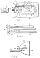
- FIG. 1 An example of an electrodeless, high-intensity discharge lamp system in accordance with the invention is shown in FIG. 1.
- the lamp system includes an electrodeless lamp assembly 10 and a high frequency source 12.
- High frequency power from the source 12 is coupled to the electrodeless lamp assembly 10 through a transmission line 14, which may for example be a coaxial cable.
- the electrodeless lamp assembly 10 includes a planar transmission line 16, electric field applicators 18 and 19, and a lamp capsule 20 having an enclosed volume containing a lamp fill material.
- the lamp capsule 20 contains a mixture of starting gas and chemical dopant material that is excitable by high frequency power to a state of luminous emission.
- the planar transmission line 16 includes a substrate 30 having a patterned conductor 34 coupled to a high frequency connector 36.
- the connector 36 is coupled via transmission line 14 to high frequency source 12.
- the conductor 34 interconnects the connector 36 and the electric field applicators 18 and 19.
- the conductor 34 is designed to provide a phase shift of 180° between applicators 18 and 19 at the frequency of source 12 and may including a tuning stub 35.
- the opposite surface of substrate 30 is covered with a conductive ground plane (not shown in FIG. 1).
- the substrate 30 is provided with a gap 38 in which the lamp capsule 20 is mounted.
- the lamp capsule 20 is spaced above the plane of substrate 30 and is aligned with the electric field applicators 18 and 19.
- Electrically conducive wires 40 and 42 may be connected between opposite sides of gap 38 to symmetrize the electric field in the region of lamp capsule 20.
- the lamp capsule 20 is mechanically supported above the surface of substrate 30 by a refractory support block 50.
- Lamp capsule 20 includes a discharge portion 52 and a lamp stem 54 that extends from one end of the discharge portion 52.
- the lamp stem 54 is cemented to support block 50, so that the lamp capsule 20 is spaced above substrate 30 in alignment with electric field applicators 18 and 19.
- the support block 50 is fabricated of a refractory material and may have the general form of a rectangular parallelepiped.
- the support block 50 includes a top surface 60 having a groove 62 and side walls 64, 65, 66 and 67.
- a groove 70 is formed in side wall 64.
- the groove 70 is dimensioned and shaped for receiving an edge 72 of substrate 30.
- the recess 62 is dimensioned and shaped for receiving lamp stem 54.
- edge 72 of substrate 30 is positioned in groove 70 and is cemented in position.
- the lamp stem 54 is cemented in recess 62 to form a rigid assembly.
- the support block 50 may be moved along the edge 72 of substrate 30 in a direction parallel to a longitudinal axis 76 of groove 70.
- lamp stem 54 may be moved parallel to a longitudinal axis 78 of recess 62 with respect to support block 50. This construction permits the position of the lamp capsule 20 to be adjusted before it is cemented into a fixed position.
- the longitudinal axis 76 of groove 70 is perpendicular to the longitudinal axis 78 of recess 62. It will be understood that at different configurations of the refractory support block 50 are included within the scope of the present invention.
- the longitudinal axis of the groove 70 may be parallel to the longitudinal axis of recess 62. In this configuration, groove 70 may be formed in one of the side walls 66 or 67.
- the relative positions of the recess 62 and groove 70 depend on the configuration of the substrate and the desired mounting position of lamp capsule 20.
- the spacing between groove 70 and recess 62 defines the spacing of lamp capsule 20 above substrate 30.
- the recess 62 may have any desired shape. In the example of FIG.
- recess 62 is formed as a V-shaped notch.
- a refractory support block 80 includes a recess 82 formed as a semicircular notch.
- the groove 70 has width W that is slightly larger than the thickness of substrate 30 and a depth D that is sufficient to permit secure attachment of the support block 50 to the edge 72 of substrate 30.
- the support block 50 is typically utilized with a planar substrate 30.
- the support block of the invention may be utilized with a substrate of any shape.
- the groove 70 is shaped to match the contour of substrate 30. For example, if the substrate has a radius of curvature, the groove 70 is provided with a matching radius of curvature.
- the support block of the present invention is fabricated of a heat-resistant, electrically-insulating material and may be required to withstand temperatures of up to 400°C.
- the support block can be made of a machinable ceramic, such as Macor, sintered from ceramic, such as polycrystalline alumina, ground from glass such as pyrex or fused silica, or molded or machined from a high temperature polymer such as Ultem.
- the refractory material should have good mechanical strength, be heat resistant, be nonmetallic and be formable.
- a preferred material is Macor, since it is easily machined. However, other materials may be used within the scope of the present invention.
- the refractory block has a width of about 0.2 inch, a thickness of about 0.125 inch and a height of about 0.28 inch.
- the groove 70 has a width W of 0.07 inch and a depth D of about 0.063 inch.
- the support block is used to support a 35 watt lamp capsule having a 2 mm interior diameter by 10 mm interior length with a support tubulation attached colinearly with the lamp axis.
- the lamp stem has a 1 mm inside diameter, a 2 mm outside diameter and is about 12 mm long.
- a transmission line includes a ground plane 90 and a microstrip line 92, each of which may be metal.
- the microstrip line 92 is spaced from ground plane 90 by an insulating support 94.
- An electrodeless lamp capsule 96 is positioned above microstrip line 92 by a refractory support block 98.
- a lamp stem 100 of lamp capsule 96 is cemented in a recess 102 in support block 98.
- An edge 104 of ground plane 92 is cemented in a groove 106 in support block 98.
- the support block 98 may have the construction shown in Figs. 2 and 3 and described above.
- FIG. 6 Yet another embodiment of the invention is illustrated in FIG. 6.
- An electrodeless lamp capsule 120 is positioned within a cavity defined by a reflector 122 and a wire mesh screen 124.
- a lamp stem 126 of lamp capsule 120 extends through reflector 122 to a support block 130.
- the lamp stem 126 is cemented in a recess in support block 130 as described above.
- Electrical energy is supplied to lamp capsule 120 by a coaxial transmission line 132 which terminates in a loop coupler 134.
- the support block 130 is secured to the edge of a substrate 136, which in turn is mounted to transmission line 132.
- the electric field applicators 18 and 19 may comprise helical couplers as disclosed in the aforementioned patent number 5,070,277; end cup applicators as disclosed in the aforementioned patent number 5,241,246; loop applicators as disclosed in the aforementioned patent number 5,130,612; or any other suitable electric field applicator.
- the electric field applicators produce a high intensity electric field within the enclosed volume of the lamp capsule, so that the applied high frequency power is absorbed by the plasma discharge.
- the high intensity discharge lamp of the present invention can operate at any frequency in the range of 13 megahertz to 20 gigahertz at which substantial power can be developed.
- the operating frequency is typically selected in one of the ISM bands.
- the frequencies centered around 915 megahertz and 2.45 gigahertz are particularly appropriate.
- the planar transmission line 16 is designed to couple high frequency power at the operating frequency to the electric field applicators 18 and 19 with 180° phase shift.
- the design and construction of planar transmission lines for transmission of high frequency power are well known to those skilled in the art.
- the substrate 30 of the planar transmission line is a dielectric material, such as for example, glass, microfiber reinforced PTFE, composite laminate or BEO having an approximate relative dielectric constant of 2.5 to 10.0 and having a thickness of 0.030 - 0.062 inch.
- the conductor 34 is patterned on one surface of the substrate, and a ground plane conductor is formed on the opposite surface of the substrate. Examples of suitable planar transmission lines include stripline and microstripline transmission lines.
Landscapes
- Physics & Mathematics (AREA)
- Electromagnetism (AREA)
- Engineering & Computer Science (AREA)
- Plasma & Fusion (AREA)
- Non-Portable Lighting Devices Or Systems Thereof (AREA)
- Fastening Of Light Sources Or Lamp Holders (AREA)
- Discharge Lamps And Accessories Thereof (AREA)
Applications Claiming Priority (2)
| Application Number | Priority Date | Filing Date | Title |
|---|---|---|---|
| US670870 | 1996-06-26 | ||
| US08/670,870 US5821698A (en) | 1996-06-26 | 1996-06-26 | Refractory block for supporting electrodeless lamp capsule |
Publications (3)
| Publication Number | Publication Date |
|---|---|
| EP0817240A2 true EP0817240A2 (fr) | 1998-01-07 |
| EP0817240A3 EP0817240A3 (fr) | 1998-03-11 |
| EP0817240B1 EP0817240B1 (fr) | 2001-11-28 |
Family
ID=24692232
Family Applications (1)
| Application Number | Title | Priority Date | Filing Date |
|---|---|---|---|
| EP97109526A Expired - Lifetime EP0817240B1 (fr) | 1996-06-26 | 1997-06-12 | Bloc réfractaire pour supporter une capsule de lampe sans électrode |
Country Status (5)
| Country | Link |
|---|---|
| US (1) | US5821698A (fr) |
| EP (1) | EP0817240B1 (fr) |
| JP (1) | JPH1064314A (fr) |
| CA (1) | CA2208881C (fr) |
| DE (1) | DE69708525T2 (fr) |
Cited By (1)
| Publication number | Priority date | Publication date | Assignee | Title |
|---|---|---|---|---|
| WO1998057356A1 (fr) * | 1997-06-10 | 1998-12-17 | Osram-Sylvania Inc. | Lampe a decharge a haute intensite sans electrodes a usage medical |
Families Citing this family (2)
| Publication number | Priority date | Publication date | Assignee | Title |
|---|---|---|---|---|
| KR20100109500A (ko) * | 2009-03-31 | 2010-10-08 | 오스람 게젤샤프트 미트 베쉬랭크터 하프퉁 | 무전극 가스 방전 램프들의 동작을 위한 장 어플리케이터들에 대한 콤팩트한 지연 라인 구조들 |
| US11705321B2 (en) * | 2019-06-12 | 2023-07-18 | Topanga Asia Limited | Electrodeless plasma lamps, transmission lines and radio frequency systems |
Family Cites Families (10)
| Publication number | Priority date | Publication date | Assignee | Title |
|---|---|---|---|---|
| US2488169A (en) * | 1946-02-20 | 1949-11-15 | Benjamin B Schneider | Neon-type sign |
| EP0457242B1 (fr) * | 1990-05-15 | 1995-08-30 | Osram Sylvania Inc. | Lampe de décharge à haute intensité sans électrode avec coupleur à raccorder à un générateur à micro-ondes |
| US5113121A (en) * | 1990-05-15 | 1992-05-12 | Gte Laboratories Incorporated | Electrodeless HID lamp with lamp capsule |
| US5070277A (en) * | 1990-05-15 | 1991-12-03 | Gte Laboratories Incorporated | Electrodless hid lamp with microwave power coupler |
| US5144206A (en) * | 1991-09-10 | 1992-09-01 | Gte Products Corporation | Electrodeless HID lamp coupling structure with integral matching network |
| US5241246A (en) * | 1991-09-10 | 1993-08-31 | Gte Laboratories Incorporated | End cup applicators for high frequency electrodeless lamps |
| US5130612A (en) * | 1991-09-11 | 1992-07-14 | Gte Products Corporation | Loop applicator for high frequency electrodeless lamps |
| JPH0643557A (ja) * | 1992-07-27 | 1994-02-18 | Sharp Corp | 露光装置 |
| JPH0682932A (ja) * | 1992-09-01 | 1994-03-25 | Sharp Corp | 画像形成装置の露光装置 |
| US5299100A (en) * | 1992-12-29 | 1994-03-29 | Gte Products Corporation | Microwave powered vehicle lamp |
-
1996
- 1996-06-26 US US08/670,870 patent/US5821698A/en not_active Expired - Lifetime
-
1997
- 1997-06-12 DE DE69708525T patent/DE69708525T2/de not_active Expired - Fee Related
- 1997-06-12 EP EP97109526A patent/EP0817240B1/fr not_active Expired - Lifetime
- 1997-06-24 CA CA002208881A patent/CA2208881C/fr not_active Expired - Fee Related
- 1997-06-26 JP JP9170090A patent/JPH1064314A/ja active Pending
Cited By (1)
| Publication number | Priority date | Publication date | Assignee | Title |
|---|---|---|---|---|
| WO1998057356A1 (fr) * | 1997-06-10 | 1998-12-17 | Osram-Sylvania Inc. | Lampe a decharge a haute intensite sans electrodes a usage medical |
Also Published As
| Publication number | Publication date |
|---|---|
| DE69708525D1 (de) | 2002-01-10 |
| EP0817240A3 (fr) | 1998-03-11 |
| JPH1064314A (ja) | 1998-03-06 |
| EP0817240B1 (fr) | 2001-11-28 |
| CA2208881C (fr) | 2005-09-06 |
| DE69708525T2 (de) | 2002-05-02 |
| CA2208881A1 (fr) | 1997-12-26 |
| US5821698A (en) | 1998-10-13 |
Similar Documents
| Publication | Publication Date | Title |
|---|---|---|
| KR101088522B1 (ko) | 무전극 플라즈마 램프 | |
| EP0684629B1 (fr) | Lampe à décharge à haute intensité sans électrodes alimentée par un champ électrique tournant | |
| US5113121A (en) | Electrodeless HID lamp with lamp capsule | |
| CN101790773B (zh) | 微波动力光源 | |
| US7880402B2 (en) | Plasma lamp with field-concentrating antenna | |
| US8405291B2 (en) | Microwave light source with solid dielectric waveguide | |
| CA1149078A (fr) | Source compacte de lumiere fluorescente a electrodes metallisees | |
| GB2048589A (en) | Supply for electrodeless discharge apparatus with double ended power coupling | |
| US3942068A (en) | Electrodeless light source with a termination fixture having an improved center conductor for arc shaping capability | |
| JPH08148127A (ja) | マイクロ波放電光源装置 | |
| RU2552107C2 (ru) | Источник света | |
| EP0457242B1 (fr) | Lampe de décharge à haute intensité sans électrode avec coupleur à raccorder à un générateur à micro-ondes | |
| CA2076813C (fr) | Electrodes d'embout pour lampes sans electrode a haute frequence | |
| US6107752A (en) | Coaxial applicators for electrodeless high intensity discharge lamps | |
| US8525430B2 (en) | Helical structure and method for plasma lamp | |
| US5821698A (en) | Refractory block for supporting electrodeless lamp capsule | |
| KR100417342B1 (ko) | 전기장대칭기구를구비한무전극고휘도방전램프 | |
| CN202103018U (zh) | 等离子体灯设备和用于等离子体灯的设备 | |
| US9177779B1 (en) | Low profile electrodeless lamps with an externally-grounded probe | |
| US5844376A (en) | Electrodeless high intensity discharge lamp with split lamp stem | |
| US8405290B2 (en) | Light source for microwave powered lamp | |
| JP2004087434A (ja) | 無電極放電ランプ光源装置 | |
| HK1143243B (en) | Microwave-powered light source | |
| JP2003272407A (ja) | 無電極放電ランプ光源装置 |
Legal Events
| Date | Code | Title | Description |
|---|---|---|---|
| PUAI | Public reference made under article 153(3) epc to a published international application that has entered the european phase |
Free format text: ORIGINAL CODE: 0009012 |
|
| AK | Designated contracting states |
Kind code of ref document: A2 Designated state(s): BE DE FR GB IT NL |
|
| PUAL | Search report despatched |
Free format text: ORIGINAL CODE: 0009013 |
|
| AK | Designated contracting states |
Kind code of ref document: A3 Designated state(s): AT BE CH DE DK ES FI FR GB GR IE IT LI LU MC NL PT SE |
|
| 17P | Request for examination filed |
Effective date: 19980406 |
|
| AKX | Designation fees paid |
Free format text: BE DE FR GB IT NL |
|
| RBV | Designated contracting states (corrected) |
Designated state(s): BE DE FR GB IT NL |
|
| 17Q | First examination report despatched |
Effective date: 19991122 |
|
| GRAG | Despatch of communication of intention to grant |
Free format text: ORIGINAL CODE: EPIDOS AGRA |
|
| GRAG | Despatch of communication of intention to grant |
Free format text: ORIGINAL CODE: EPIDOS AGRA |
|
| GRAH | Despatch of communication of intention to grant a patent |
Free format text: ORIGINAL CODE: EPIDOS IGRA |
|
| GRAH | Despatch of communication of intention to grant a patent |
Free format text: ORIGINAL CODE: EPIDOS IGRA |
|
| GRAA | (expected) grant |
Free format text: ORIGINAL CODE: 0009210 |
|
| AK | Designated contracting states |
Kind code of ref document: B1 Designated state(s): BE DE FR GB IT NL |
|
| REG | Reference to a national code |
Ref country code: GB Ref legal event code: IF02 |
|
| REF | Corresponds to: |
Ref document number: 69708525 Country of ref document: DE Date of ref document: 20020110 |
|
| ET | Fr: translation filed | ||
| PLBE | No opposition filed within time limit |
Free format text: ORIGINAL CODE: 0009261 |
|
| STAA | Information on the status of an ep patent application or granted ep patent |
Free format text: STATUS: NO OPPOSITION FILED WITHIN TIME LIMIT |
|
| 26N | No opposition filed | ||
| PGFP | Annual fee paid to national office [announced via postgrant information from national office to epo] |
Ref country code: NL Payment date: 20030619 Year of fee payment: 7 |
|
| PGFP | Annual fee paid to national office [announced via postgrant information from national office to epo] |
Ref country code: BE Payment date: 20030624 Year of fee payment: 7 |
|
| PGFP | Annual fee paid to national office [announced via postgrant information from national office to epo] |
Ref country code: FR Payment date: 20030627 Year of fee payment: 7 |
|
| PG25 | Lapsed in a contracting state [announced via postgrant information from national office to epo] |
Ref country code: BE Free format text: LAPSE BECAUSE OF NON-PAYMENT OF DUE FEES Effective date: 20040630 |
|
| BERE | Be: lapsed |
Owner name: *OSRAM SYLVANIA INC. Effective date: 20040630 |
|
| PG25 | Lapsed in a contracting state [announced via postgrant information from national office to epo] |
Ref country code: NL Free format text: LAPSE BECAUSE OF NON-PAYMENT OF DUE FEES Effective date: 20050101 |
|
| PG25 | Lapsed in a contracting state [announced via postgrant information from national office to epo] |
Ref country code: FR Free format text: LAPSE BECAUSE OF NON-PAYMENT OF DUE FEES Effective date: 20050228 |
|
| NLV4 | Nl: lapsed or anulled due to non-payment of the annual fee |
Effective date: 20050101 |
|
| REG | Reference to a national code |
Ref country code: FR Ref legal event code: ST |
|
| PGFP | Annual fee paid to national office [announced via postgrant information from national office to epo] |
Ref country code: GB Payment date: 20050607 Year of fee payment: 9 |
|
| PG25 | Lapsed in a contracting state [announced via postgrant information from national office to epo] |
Ref country code: IT Free format text: LAPSE BECAUSE OF NON-PAYMENT OF DUE FEES Effective date: 20050612 |
|
| PGFP | Annual fee paid to national office [announced via postgrant information from national office to epo] |
Ref country code: DE Payment date: 20050822 Year of fee payment: 9 |
|
| PG25 | Lapsed in a contracting state [announced via postgrant information from national office to epo] |
Ref country code: GB Free format text: LAPSE BECAUSE OF NON-PAYMENT OF DUE FEES Effective date: 20060612 |
|
| PG25 | Lapsed in a contracting state [announced via postgrant information from national office to epo] |
Ref country code: DE Free format text: LAPSE BECAUSE OF NON-PAYMENT OF DUE FEES Effective date: 20070103 |
|
| GBPC | Gb: european patent ceased through non-payment of renewal fee |
Effective date: 20060612 |