EP0817253A2 - Befestigung von Kühlkörpern direkt auf Flipchips und Keramik-Chipträgern - Google Patents
Befestigung von Kühlkörpern direkt auf Flipchips und Keramik-Chipträgern Download PDFInfo
- Publication number
- EP0817253A2 EP0817253A2 EP97303096A EP97303096A EP0817253A2 EP 0817253 A2 EP0817253 A2 EP 0817253A2 EP 97303096 A EP97303096 A EP 97303096A EP 97303096 A EP97303096 A EP 97303096A EP 0817253 A2 EP0817253 A2 EP 0817253A2
- Authority
- EP
- European Patent Office
- Prior art keywords
- adhesive
- semiconductor chips
- flexible
- epoxy
- wiring
- Prior art date
- Legal status (The legal status is an assumption and is not a legal conclusion. Google has not performed a legal analysis and makes no representation as to the accuracy of the status listed.)
- Withdrawn
Links
Images


Classifications
-
- H—ELECTRICITY
- H10—SEMICONDUCTOR DEVICES; ELECTRIC SOLID-STATE DEVICES NOT OTHERWISE PROVIDED FOR
- H10W—GENERIC PACKAGES, INTERCONNECTIONS, CONNECTORS OR OTHER CONSTRUCTIONAL DETAILS OF DEVICES COVERED BY CLASS H10
- H10W72/00—Interconnections or connectors in packages
- H10W72/30—Die-attach connectors
-
- H—ELECTRICITY
- H10—SEMICONDUCTOR DEVICES; ELECTRIC SOLID-STATE DEVICES NOT OTHERWISE PROVIDED FOR
- H10W—GENERIC PACKAGES, INTERCONNECTIONS, CONNECTORS OR OTHER CONSTRUCTIONAL DETAILS OF DEVICES COVERED BY CLASS H10
- H10W99/00—Subject matter not provided for in other groups of this subclass
-
- H—ELECTRICITY
- H10—SEMICONDUCTOR DEVICES; ELECTRIC SOLID-STATE DEVICES NOT OTHERWISE PROVIDED FOR
- H10W—GENERIC PACKAGES, INTERCONNECTIONS, CONNECTORS OR OTHER CONSTRUCTIONAL DETAILS OF DEVICES COVERED BY CLASS H10
- H10W40/00—Arrangements for thermal protection or thermal control
- H10W40/20—Arrangements for cooling
- H10W40/22—Arrangements for cooling characterised by their shape, e.g. having conical or cylindrical projections
-
- H—ELECTRICITY
- H10—SEMICONDUCTOR DEVICES; ELECTRIC SOLID-STATE DEVICES NOT OTHERWISE PROVIDED FOR
- H10W—GENERIC PACKAGES, INTERCONNECTIONS, CONNECTORS OR OTHER CONSTRUCTIONAL DETAILS OF DEVICES COVERED BY CLASS H10
- H10W40/00—Arrangements for thermal protection or thermal control
- H10W40/70—Fillings or auxiliary members in containers or in encapsulations for thermal protection or control
- H10W40/77—Auxiliary members characterised by their shape
-
- H—ELECTRICITY
- H10—SEMICONDUCTOR DEVICES; ELECTRIC SOLID-STATE DEVICES NOT OTHERWISE PROVIDED FOR
- H10W—GENERIC PACKAGES, INTERCONNECTIONS, CONNECTORS OR OTHER CONSTRUCTIONAL DETAILS OF DEVICES COVERED BY CLASS H10
- H10W74/00—Encapsulations, e.g. protective coatings
- H10W74/01—Manufacture or treatment
- H10W74/012—Manufacture or treatment of encapsulations on active surfaces of flip-chip devices, e.g. forming underfills
-
- H—ELECTRICITY
- H10—SEMICONDUCTOR DEVICES; ELECTRIC SOLID-STATE DEVICES NOT OTHERWISE PROVIDED FOR
- H10W—GENERIC PACKAGES, INTERCONNECTIONS, CONNECTORS OR OTHER CONSTRUCTIONAL DETAILS OF DEVICES COVERED BY CLASS H10
- H10W74/00—Encapsulations, e.g. protective coatings
- H10W74/10—Encapsulations, e.g. protective coatings characterised by their shape or disposition
- H10W74/15—Encapsulations, e.g. protective coatings characterised by their shape or disposition on active surfaces of flip-chip devices, e.g. underfills
-
- H—ELECTRICITY
- H10—SEMICONDUCTOR DEVICES; ELECTRIC SOLID-STATE DEVICES NOT OTHERWISE PROVIDED FOR
- H10W—GENERIC PACKAGES, INTERCONNECTIONS, CONNECTORS OR OTHER CONSTRUCTIONAL DETAILS OF DEVICES COVERED BY CLASS H10
- H10W70/00—Package substrates; Interposers; Redistribution layers [RDL]
- H10W70/60—Insulating or insulated package substrates; Interposers; Redistribution layers
- H10W70/62—Insulating or insulated package substrates; Interposers; Redistribution layers characterised by their interconnections
- H10W70/63—Vias, e.g. via plugs
-
- H—ELECTRICITY
- H10—SEMICONDUCTOR DEVICES; ELECTRIC SOLID-STATE DEVICES NOT OTHERWISE PROVIDED FOR
- H10W—GENERIC PACKAGES, INTERCONNECTIONS, CONNECTORS OR OTHER CONSTRUCTIONAL DETAILS OF DEVICES COVERED BY CLASS H10
- H10W70/00—Package substrates; Interposers; Redistribution layers [RDL]
- H10W70/60—Insulating or insulated package substrates; Interposers; Redistribution layers
- H10W70/62—Insulating or insulated package substrates; Interposers; Redistribution layers characterised by their interconnections
- H10W70/65—Shapes or dispositions of interconnections
- H10W70/654—Top-view layouts
- H10W70/655—Fan-out layouts
-
- H—ELECTRICITY
- H10—SEMICONDUCTOR DEVICES; ELECTRIC SOLID-STATE DEVICES NOT OTHERWISE PROVIDED FOR
- H10W—GENERIC PACKAGES, INTERCONNECTIONS, CONNECTORS OR OTHER CONSTRUCTIONAL DETAILS OF DEVICES COVERED BY CLASS H10
- H10W72/00—Interconnections or connectors in packages
- H10W72/071—Connecting or disconnecting
- H10W72/073—Connecting or disconnecting of die-attach connectors
- H10W72/07331—Connecting techniques
-
- H—ELECTRICITY
- H10—SEMICONDUCTOR DEVICES; ELECTRIC SOLID-STATE DEVICES NOT OTHERWISE PROVIDED FOR
- H10W—GENERIC PACKAGES, INTERCONNECTIONS, CONNECTORS OR OTHER CONSTRUCTIONAL DETAILS OF DEVICES COVERED BY CLASS H10
- H10W72/00—Interconnections or connectors in packages
- H10W72/30—Die-attach connectors
- H10W72/351—Materials of die-attach connectors
- H10W72/352—Materials of die-attach connectors comprising metals or metalloids, e.g. solders
-
- H—ELECTRICITY
- H10—SEMICONDUCTOR DEVICES; ELECTRIC SOLID-STATE DEVICES NOT OTHERWISE PROVIDED FOR
- H10W—GENERIC PACKAGES, INTERCONNECTIONS, CONNECTORS OR OTHER CONSTRUCTIONAL DETAILS OF DEVICES COVERED BY CLASS H10
- H10W72/00—Interconnections or connectors in packages
- H10W72/30—Die-attach connectors
- H10W72/351—Materials of die-attach connectors
- H10W72/353—Materials of die-attach connectors not comprising solid metals or solid metalloids, e.g. ceramics
- H10W72/354—Materials of die-attach connectors not comprising solid metals or solid metalloids, e.g. ceramics comprising polymers
-
- H—ELECTRICITY
- H10—SEMICONDUCTOR DEVICES; ELECTRIC SOLID-STATE DEVICES NOT OTHERWISE PROVIDED FOR
- H10W—GENERIC PACKAGES, INTERCONNECTIONS, CONNECTORS OR OTHER CONSTRUCTIONAL DETAILS OF DEVICES COVERED BY CLASS H10
- H10W72/00—Interconnections or connectors in packages
- H10W72/50—Bond wires
- H10W72/551—Materials of bond wires
- H10W72/552—Materials of bond wires comprising metals or metalloids, e.g. silver
- H10W72/5522—Materials of bond wires comprising metals or metalloids, e.g. silver comprising gold [Au]
-
- H—ELECTRICITY
- H10—SEMICONDUCTOR DEVICES; ELECTRIC SOLID-STATE DEVICES NOT OTHERWISE PROVIDED FOR
- H10W—GENERIC PACKAGES, INTERCONNECTIONS, CONNECTORS OR OTHER CONSTRUCTIONAL DETAILS OF DEVICES COVERED BY CLASS H10
- H10W72/00—Interconnections or connectors in packages
- H10W72/50—Bond wires
- H10W72/551—Materials of bond wires
- H10W72/552—Materials of bond wires comprising metals or metalloids, e.g. silver
- H10W72/5524—Materials of bond wires comprising metals or metalloids, e.g. silver comprising aluminium [Al]
-
- H—ELECTRICITY
- H10—SEMICONDUCTOR DEVICES; ELECTRIC SOLID-STATE DEVICES NOT OTHERWISE PROVIDED FOR
- H10W—GENERIC PACKAGES, INTERCONNECTIONS, CONNECTORS OR OTHER CONSTRUCTIONAL DETAILS OF DEVICES COVERED BY CLASS H10
- H10W72/00—Interconnections or connectors in packages
- H10W72/851—Dispositions of multiple connectors or interconnections
- H10W72/853—On the same surface
- H10W72/856—Bump connectors and die-attach connectors
-
- H—ELECTRICITY
- H10—SEMICONDUCTOR DEVICES; ELECTRIC SOLID-STATE DEVICES NOT OTHERWISE PROVIDED FOR
- H10W—GENERIC PACKAGES, INTERCONNECTIONS, CONNECTORS OR OTHER CONSTRUCTIONAL DETAILS OF DEVICES COVERED BY CLASS H10
- H10W72/00—Interconnections or connectors in packages
- H10W72/851—Dispositions of multiple connectors or interconnections
- H10W72/874—On different surfaces
- H10W72/877—Bump connectors and die-attach connectors
-
- H—ELECTRICITY
- H10—SEMICONDUCTOR DEVICES; ELECTRIC SOLID-STATE DEVICES NOT OTHERWISE PROVIDED FOR
- H10W—GENERIC PACKAGES, INTERCONNECTIONS, CONNECTORS OR OTHER CONSTRUCTIONAL DETAILS OF DEVICES COVERED BY CLASS H10
- H10W72/00—Interconnections or connectors in packages
- H10W72/851—Dispositions of multiple connectors or interconnections
- H10W72/874—On different surfaces
- H10W72/884—Die-attach connectors and bond wires
-
- H—ELECTRICITY
- H10—SEMICONDUCTOR DEVICES; ELECTRIC SOLID-STATE DEVICES NOT OTHERWISE PROVIDED FOR
- H10W—GENERIC PACKAGES, INTERCONNECTIONS, CONNECTORS OR OTHER CONSTRUCTIONAL DETAILS OF DEVICES COVERED BY CLASS H10
- H10W74/00—Encapsulations, e.g. protective coatings
-
- H—ELECTRICITY
- H10—SEMICONDUCTOR DEVICES; ELECTRIC SOLID-STATE DEVICES NOT OTHERWISE PROVIDED FOR
- H10W—GENERIC PACKAGES, INTERCONNECTIONS, CONNECTORS OR OTHER CONSTRUCTIONAL DETAILS OF DEVICES COVERED BY CLASS H10
- H10W90/00—Package configurations
- H10W90/701—Package configurations characterised by the relative positions of pads or connectors relative to package parts
- H10W90/721—Package configurations characterised by the relative positions of pads or connectors relative to package parts of bump connectors
- H10W90/724—Package configurations characterised by the relative positions of pads or connectors relative to package parts of bump connectors between a chip and a stacked insulating package substrate, interposer or RDL
-
- H—ELECTRICITY
- H10—SEMICONDUCTOR DEVICES; ELECTRIC SOLID-STATE DEVICES NOT OTHERWISE PROVIDED FOR
- H10W—GENERIC PACKAGES, INTERCONNECTIONS, CONNECTORS OR OTHER CONSTRUCTIONAL DETAILS OF DEVICES COVERED BY CLASS H10
- H10W90/00—Package configurations
- H10W90/701—Package configurations characterised by the relative positions of pads or connectors relative to package parts
- H10W90/731—Package configurations characterised by the relative positions of pads or connectors relative to package parts of die-attach connectors
- H10W90/734—Package configurations characterised by the relative positions of pads or connectors relative to package parts of die-attach connectors between a chip and a stacked insulating package substrate, interposer or RDL
-
- H—ELECTRICITY
- H10—SEMICONDUCTOR DEVICES; ELECTRIC SOLID-STATE DEVICES NOT OTHERWISE PROVIDED FOR
- H10W—GENERIC PACKAGES, INTERCONNECTIONS, CONNECTORS OR OTHER CONSTRUCTIONAL DETAILS OF DEVICES COVERED BY CLASS H10
- H10W90/00—Package configurations
- H10W90/701—Package configurations characterised by the relative positions of pads or connectors relative to package parts
- H10W90/731—Package configurations characterised by the relative positions of pads or connectors relative to package parts of die-attach connectors
- H10W90/736—Package configurations characterised by the relative positions of pads or connectors relative to package parts of die-attach connectors between a chip and a stacked lead frame, conducting package substrate or heat sink
-
- H—ELECTRICITY
- H10—SEMICONDUCTOR DEVICES; ELECTRIC SOLID-STATE DEVICES NOT OTHERWISE PROVIDED FOR
- H10W—GENERIC PACKAGES, INTERCONNECTIONS, CONNECTORS OR OTHER CONSTRUCTIONAL DETAILS OF DEVICES COVERED BY CLASS H10
- H10W90/00—Package configurations
- H10W90/701—Package configurations characterised by the relative positions of pads or connectors relative to package parts
- H10W90/751—Package configurations characterised by the relative positions of pads or connectors relative to package parts of bond wires
- H10W90/754—Package configurations characterised by the relative positions of pads or connectors relative to package parts of bond wires between a chip and a stacked insulating package substrate, interposer or RDL
-
- H—ELECTRICITY
- H10—SEMICONDUCTOR DEVICES; ELECTRIC SOLID-STATE DEVICES NOT OTHERWISE PROVIDED FOR
- H10W—GENERIC PACKAGES, INTERCONNECTIONS, CONNECTORS OR OTHER CONSTRUCTIONAL DETAILS OF DEVICES COVERED BY CLASS H10
- H10W90/00—Package configurations
- H10W90/701—Package configurations characterised by the relative positions of pads or connectors relative to package parts
- H10W90/751—Package configurations characterised by the relative positions of pads or connectors relative to package parts of bond wires
- H10W90/756—Package configurations characterised by the relative positions of pads or connectors relative to package parts of bond wires between a chip and a stacked lead frame, conducting package substrate or heat sink
Definitions
- This invention relates to the production of electronic components, the assembly of components to circuitized substrates to form circuit boards, and the assembly of the circuit boards with a power supply to provide information handling systems. More particularly, these inventions are most closely relates to the art of attaching heat spreaders or heat sinks to electronic components and the resulting structures.
- the heat generated in the components is conducted by a thermal path through the component terminals into a circuitized card substrate (most commonly fibreglass filled epoxy) and through the wiring layers of the card.
- the card dissipates the heat by convection to the surrounding air, and by radiation to the enclosure containing the board, and through card connectors and supports to other boards or the enclosure.
- some of the generated heat is removed through the back side of the component by convection to the surrounding atmosphere and to a lesser extent, radiation to any cooler surfaces surrounding the card.
- thermal greases are typically thick organic liquids (such as silicon oils) filled with particles of a highly thermoconductive material such as alumina, beryllium, copper, silver, or graphite.
- CPGAs ceramic PGAs
- a heat sink e.g. aluminium Al or copper Cu
- a component e.g. aluminium Al or copper Cu
- Thermal grease is usually provided to fill voids between the heat sink and the component since even a very thin air gap becomes a significant resistance layer in the thermal path.
- individual power transistors have been supplied potted in T0 - T3 cans by silicon or epoxy potting compound. Again such adhesives have been filled with thermoconductive materials to increase thermal conduction and reduce the temperature of the semiconductor devices.
- Such discrete power transistors have also been supplied in a small thin package with a hole for screwed connection to circuit boards with thermal grease provided between the transistor and board. Also, simple heat sinks of bent plate, have been provided to increase thermal performance.
- Integrated circuit components are characterised by large numbers of input and output I/O connection terminals.
- Organic materials have been used extensively in production of such integrated electronic components.
- Most common components are manufactured by producing a lead frame on a polyimide tape, using an adhesive (e.g. epoxy or silicon adhesives) to connect the back side of a wire bond chip onto the lead frame tape and wire bonding to connect the front of the die to the leads of the frame.
- the adhesives manufactured for connecting chips to polyimide tape are usually filled with thermoconductive particles to increase heat conduction from the chip and thus minimise chip temperature.
- Plastic components are usually manufactured by transfer molding to encapsulate the chip, bond wires, and part of the leads with epoxy to form a plastic substrate.
- Ceramic components are usually manufactured by providing a cavity under a ceramic substrate into which the chip, bond wires are placed and then the polyimide tape is adhesively bonded to the ceramic substrate with epoxy or silicon adhesives and the chip and cavity is filled with thermoconductive epoxy or silicon adhesive.
- a ceramic bottom substrate may be bonded over the bottom of the cavity to protect the bottom of the component.
- Heat sinks have usually been connected to integrated packages by screwing or clipping.
- Non-silicon greases are commonly used between the heat sink and the modules to increase thermal performance.
- the heat sinks are usually connected to integrated components after circuit board assembly.
- Recently in order to reduce costs, manufacturers have started adhesively bonding heat sinks directly to organic or ceramic surfaces of electronic components after circuit board assembly using epoxy based materials. Since the coefficient of thermal expansion CTE of epoxy is around 50-80 ppm/°C and the CTE of Al is 26.4 ppm/°C and copper is 17 ppm/°C and the coatings used for heat sinks (bare copper, nickel coated copper, bare Al, anodized Al, chromium conversion on Al) are smooth and do not adhere well to epoxy, it is difficult to maintain bonding during thermal cycling.
- the epoxy used for heat sink attach is filled with thermoconductive metal or ceramic particles that modify the CTE of the adhesive to a level (e.g. 30 - 40 ppm/°C) which is midway between that of the module material (epoxy) and that of the base metal of the heat sink.
- silicon adhesives have been suggested to connect anodized Al heat sinks to ceramic surfaces of modules because silicone based adhesives are very heat resistant. Silicone based adhesives have Tg's below 25°C and Young's Modulus below 14.06x10 5 kg/m 2 (2,000 psi) and are thus, very compliant. However silicon has a very high coefficient of thermal expansion of around 200 ppm, and it is difficult to provide reliable bonds between silicon and common heat sink surfaces. Mechanically, the bond strengths between silicon adhesive and these metal surfaces are about one third to one half the strength of epoxy.
- Silicon is a weak material with a tensile strength of only about 3.5 x 10 5 kg/m 2 (500 psi) versus about 14 x 10 5 kg/m 2 (2,000 psi) for epoxy.
- constituents of silicon adhesives have a tendency to migrate out contaminating surfaces with a micro thin coating which prevents subsequent attachment of other organic materials to the circuit boards such as photoresists, solder resists, and encapsulants.
- heat sinks are attached after other process for constructing circuit boards is complete thus minimising contamination problems during construction. Contamination is especially a problem for reworked components because heating the silicon during rework greatly increases the contamination and prevents any subsequent encapsulation or other non-silicon processes on the circuit board that may be required for rework.
- U.S. Patent 4,000,509 to Jarvela describes using thermal grease to thermally connect a flip chip to a heat sink.
- U.S. Patent 5,271,150 to Inasaka describes manufacture of ceramic substrates.
- U.S. patent 4,701,482 to Itoh describe using epoxy to encapsulate C4 joints.
- U.S. patent 5,159,535 to Desai describes attaching the back of flip chips to a substrate.
- European Patent Application 93104433.3 to Bennett discloses a semiconductor die attached to a lead frame.
- Patent 4,914,551 to Anschel discloses attaching a semiconductor chip to a heat spreader of silicon carbide (SiC), aluminium nitride (AlN), or Cu-Invar-Cu using epoxy. Removal of Heat From Direct Chip Attach Circuitry by G. Schrottke and D.J. Willson in IBM Technical Disclosure Bulletin Volume 32 Number 4A September, 1989, discloses using adhesive to bond silicon chips to a Cu-Invar-Cu heat spreader.
- U.S. patent 5,168,430 to Nitsch in Fig. 2 shows a hybrid circuit structure 3 cemented to a heat spreader 4.
- Technical Data Sheet for Ablebond P1-8971 by Ablestik of 9/93 recommends attaching a large die to a silver coated copper lead frame using flexible epoxy.
- Product Data Sheet for Prima-Bond EG 7655 by A.I. Technology, Inc. recommends bonding Alumina to Aluminium and Silicon to Copper.
- New Product Description for X3-6325 by Dow Corning 1994 suggests a silicon adhesive "used for bonding, sealing and adhering substrates lids and heat sinks.”
- Information About High Technology Silicon Materials by Dow Coming 1988 suggest using SYLGARD Q3-6605 silicon adhesive for attaching "hybrid integrated circuit substrates, components and devices to heat sinks.”
- Semiconductor Packaging Materials Selector Guide by General Electric suggests using RTV6424 a silicon adhesive, "for die-attach applications” MS-523 Silicone Technical Bulletin by Thermoset Plastics. Inc.
- U.S. patents 5,159,535 to Desai; 5,278,724 to Angulas; 5,147,084 to Behum suggest various flip chip carrying modules. Optimization of Thermal Adhesive Bond Strength for Extended use of TBGA at Elevated Temperatures by Bernier and Memis at NEPCON West Anaheim CA, March 1995.
- a silicon adhesive in which low molecular weight cyclic compounds have been stripped out (e.g. by a heat vaporization process) and by attaching the heat sink to a component and
- a thin layer of a highly flexible-epoxy that has a glass transition temperature below room temperature can be used to bond the heat spreader directly to the back of a flip-chip or a ceramic surface and the bond will remain strong even after thermal cycle testing of 0 to 100°C for 1500 cycles, -25 to 125°C for 400 cycles, and -40 to 140°C for 300 cycles; or after continuous exposure to 130 degrees C for 1000 hours, and still retain a strength of at least 3.5 x 10 5 kg/m 2 (500 psi).
- silicon or flexible-epoxy adhesive attach an aluminium or copper heat sink to the back side of a flip chip.
- flexible-epoxy connects an aluminium or copper heat spreader to a ceramic substrate.
- Typical silicons include significant amounts of silicon compounds (e.g. cyclic compounds) which vaporise during reflow heating and contaminate surrounding surfaces. Contamination of surrounding surfaces can be reduced by using a silicon adhesive in which low molecular weight silicon compounds (cyclic compounds) have been stripped out (e.g. by a heat vaporization process) so that contamination does not significantly effect subsequent reworking. Also, attaching heat sinks to components and baking at high temperatures (200-220°C) before connection to the circuit board reduces contamination during subsequent reworking at the same or lower temperatures.
- silicon compounds e.g. cyclic compounds
- Contamination of surrounding surfaces can be reduced by using a silicon adhesive in which low molecular weight silicon compounds (cyclic compounds) have been stripped out (e.g. by a heat vaporization process) so that contamination does not significantly effect subsequent reworking.
- attaching heat sinks to components and baking at high temperatures (200-220°C) before connection to the circuit board reduces contamination during subsequent reworking at the same or lower temperatures.
- the amount of silicon compounds which vaporizes during reflow baking is less than 10% and more preferably less than 1% of the amount that vaporizes when typical silicon adhesives are cured and then baked sufficient to reflow eutectic Pb/Sn solder (200°C) for component removal and then for component replacement.
- the amount of vaporizable materials in the cured silicon used in the invention is less then 10% and more preferably less than 1% of the levels of such materials in typical unbaked silicon adhesives.
- none of the constituents of the cured silicon significantly vaporizes to produce small voids in the adhesive, up to a temperature of 200°C.
- a suitable silicon adhesive is TC3280G which is available from General Electric Company NY.
- Typical epoxies have a Tg of about 140 - 150 degrees C, but flexible-epoxies used in these inventions have a Tg below about 25°, preferably below 10°C and more preferably below 0°C.
- typical epoxies have a Young's modulus of around 7.03 x 10 8 kg/m 2 (1,000,000 psi) but flexible-epoxies used in the present invention have a Young's modulus below about 7.03 x 10 8 kg/m 2 (100,000 psi), preferably below 35 x 10 6 kg/m 2 (50,000 psi), and even more preferably below 14.0 6 x 10⁶ kg/m 2 (20,000 psi).
- a two part flexible-epoxy named Prima-Bond EG 7655 is available from AI Technologies Inc. 9 Princess Rd. Lawrencevill, N.J. 08648 and has a Tg of about -25°C and a Young's modulus less than about 14.06 x 10 6 kg/m 2 (20,000 psi).
- a one part flexible-epoxy named ABLEBOND P1 - 8971 is distributed by Ablestick Laboratories 20021 Susana Road Rancho Dominguez, CA 90221. and has a Tg of about 5°C and a Young's modulus of less than about 35 x 10 6 kg/m 2 (50,000 psi).
- the silicon adhesive is more preferred for higher temperature applications such as attaching directly to flip chips, where temperatures could exceed 130°C and the flexible-epoxy is more preferred for less critical applications such as attaching heat sinks to ceramic surfaces.
- One common performance specification for electronic components is storage at 150°C for 1000 hours.
- the flexible-epoxy's of this invention can not undergo that test and still reliably provide 35 x 10 4 kg/m 2 (500 psi) of tensile strength without delamination, but the silicon adhesive meets these requirements.
- the CQFP module is produced from two preformed, fired halves 100, 102 of ceramic (preferably Al-N).
- Semiconductor chip 106 preferably silicon
- top half 100 of the flat pack using for example a typical die attach epoxy 108
- the chip is wire bonded 112 to the lead frame.
- the bond wires are gold or more commonly aluminium wires extending between aluminium or gold plated pads.
- top half 100 is bonded to bottom half 102 using for example a typical epoxy 110, 114.
- Cavity 116 is typically empty but may contain a dielectric, thermoconductive potting material (e.g. silicon grease).
- an Aluminium heat spreader 118 with a clean Al metal surface is attached to the top of the ceramic module using a thin layer of flexible-epoxy 120.
- the surface of the aluminium is preferably treated to increase adhe sion with the flexible-epoxy.
- the surface can be roughened by vapor blasting, grit blasting, etching or a similar roughening finishing can be used to increase adhesion of flexible-epoxy to aluminium.
- the CTE of Al-N is about 4.6 ppm/°C
- the CTE of the Al of the heat spreader is about 23.6 ppm/°C, which results in a CTE difference of 19 ppm/°C.
- the ceramic top is a relatively smooth surface and any de-lamination or cracking of the epoxy between the package and heat spreader causes a critical reduction in heat transfer from the chip.
- a common industry test is to subject components with bonded heat sinks to thermal cycling of 0 to 100°C for 1500 cycles, -25 to 125°C for 400 cycles, and -40 to 140°C for 300 cycles, or continuous exposure to 130 degrees C for 1000 hours.
- the applicants have discovered that flexible-epoxies (e.g. ABLEBOND P1-8971 from Ablestik and Prima-Bond EG 7655 from A.I. Technology Inc. of Trenton, NJ) meet the thermal cycling requirements of this test.
- cap 102 may be replaced by an encapsulant (gob top of epoxy) to protect the wire bond chip.
- the epoxy may just cover the chip and wire bonds or it may extend to the circuit board on which the module is mounted.
- an organic material such as fiberglass-epoxy or a laminate of copper and polyimide foils may be substituted for the ceramic of the top half 100.
- Fig. 2 shows another CQFP 148 which does not have a ceramic cover.
- the front side (bottom) of a semiconductor flip-chip die 150 is attached to a single layer rectangular ceramic chip carrier 152 by a perimeter row or an area array of joints 154 that extend between conductive contacts on the chip to conductive contacts on the carrier.
- the joints may be C4 joints or eutectic solder or joints of electrically conductive adhesive ECA such as thermoplastic adhesive filled with high melting temperature electroconductive particles (e.g. silver or copper or silver coated particles) or transient liquid phase TLP system particles.
- ECA electrically conductive adhesive
- the chip is passivated with a layer of polyimide or glass with windows exposing small aluminium pads of the wiring layer. Then the windows are covered with larger surface pads comprising layers of chromium, copper, and aluminium.
- the pads are covered with hemispheres of high temperature solder (Pb and 3-15% Sn more preferably 3-10% Sn) by dry deposition or electroplating or screening solder paste and reflow or by liquid solder injection.
- the chip with C4 bumps may be directly connected to copper pads on a ceramic carrier substrate by the C4 process.
- the C4 bumps may be connected to copper pads on an organic coated carrier substrate using eutectic solder deposited on the C4 bumps or on the 35 carrier pads.
- pads on the chip or on the organic coated substrate may be bumped with eutectic solder (e.g. Pb and 35-85% Sn more preferably about 70% Sn).
- TLP system particles are particles of a noble metal base coated with a reactive metal or reactive metal base coated with noble metal.
- the metals in common solder systems can be used to form TLP systems.
- the amount of the coating metal is restricted with respect to the base metal so that when the material is heated the coating alloys with part of the base to form a molten eutectic coating which connects particles together but as the base continues to dissolve into the coating even at constant temperature, the proportions of the metal alloy change until the coating resolidifies.
- the chip bumps could be attached to the contacts on the carrier by eutectic solder bumps deposited by plating, solder inject, or transfer from a decal.
- Leads such as gull wing leads 156 are clipped to a peripheral row of copper pads 158 along two or more preferably all four edges (for QFPs) of the component and soldered 158 for surface mount connection to substrate 159. Alternately, the bottom end of the leads may bend under the module in a J or even pointed strait down in an I shape.
- the leads are connected to pads 170 of metal (such as copper) on substrate 159 by solder such as Pb/Sn 37/63% by weight.
- the substrate is a ceramic such as alumina or beryllium.
- the substrate may be a rigid organic substrate such as fiberglass filled epoxy, or metal coated substrate such as Covar or Invar or Cu-Invar-Cu coated with polyimide film or a flexible circuit board substrate such as laminated layers of copper and polyimide.
- the chip connection joints 154 are encapsulated with epoxy 160 and preferably the lead clip connections are encapsulated with epoxy 162.
- an epoxy coating 164 is applied so to protect the top layer ceramic circuitry (a conformal coating which is the same level at the top of the chip).
- Heat spreader 164 (of anodized aluminum) is attached to the back side of chip 150 using adhesive 166 of flexible-epoxy or more preferably a silicon adhesive.
- Improved mechanical strength may be obtained for heat spreaders that have a footprint much larger than the chip, by also bonding the heat spreader to the conformal coating at 168 with a typical epoxy or preferably with a flexible-epoxy. Encapsulating the silicon adhesive with epoxy reduces contamination of the circuit board during subsequent rework.
- the CTE of Si metal is about 2.6 ppm/°C and the CTE of the Al of the heat spreader is about 23.6 ppm/°C which results in a CTE difference of 21 ppm/°C.
- the back of the chip is very smooth resulting in a weak mechanical bond and any de-lamination of the epoxy between the chip and heat spreader would cause a critical reduction in heat transfer from the chip and resulting extreme increase in chip temperature and failure.
- Fig. 3 shows a CPGA (ceramic pin grid array module) 200.
- the front side (bottom) of a semiconductor flip-chip die 202 is attached to a rectangular ceramic chip carrier 204 (single or multi-layer as shown) by a perimeter row or area array of joints 206.
- substrate 204 may be organic or metal coated with organic.
- a matrix of pins 208 are wave soldered 210 to copper pads 212 on both end of PTHs (plated-through-holes) extending through substrate 214 (e.g. fiberglass epoxy or flexible laminate of copper-polyimide films).
- Joints 206 are encapsulated with epoxy 220 and heat spreader 224 is attached to the back side of chip 202 using adhesive 226 of flexible-epoxy or more preferably silicon.
- Fig. 4 shows a BGA (ball grid array) module 240 which is similar to the CPGA of Fig. 3.
- Substrate 242 may be ceramic (CBGA) or plastic (PBGA) and may be single layer or multi-layer as shown.
- adhesive 244 of flexible-epoxy or more preferably silicon is used to attach heat sink 246 to flip-chip 248. In this case the heat sink is only slightly larger than the chip and the attach adhesive does not extend significantly between the heat sink and the conformal coating.
- Fig. 5 shows TBGA module 250.
- the bottom (front side) of flip-chip 252 is attached to copper pads 254 of a flexible chip carrier substrate 256.
- the substrate is laminate of one or more patterned copper films and polyimide films.
- the copper may be dry deposited on the polyimide and then photolithograhically patterned or patterned foils of copper may be laminated to dry polyimide films.
- Joints 258 may be formed by a C4 process, by C4 bumps eutectic soldered to the pads, by thermal compression bonding C4 bumps to gold pads, by laser welding, or by the SATT (solder attach tape technology).
- Rectangular metal frame 262 such as Al or preferably Cu plated by nickel (Ni), is attached to the flex substrate by adhesive 264 (preferably epoxy).
- Heat spreader 270 is a flat plate attached to frame 262 by adhesive 272 (preferably epoxy) and is attached to chip 252 by adhesive 254 of flexible-epoxy or more preferably silicon.
- the heat spreader may be Al which may be treated by anodization or coated with chromium more preferably is Cu which may be treated by chromate conversion of more Preferably coated with Ni.
- the nickel coating may be formed on clean copper by electrolessly plating or electroplating.
- the nickel coating is ultrasonically cleaned in isopropyl alcohol, rinsed with hot deionized water, exposed to hot hydrogen peroxide (30% solution at 40-100âC preferably about 70-85âC) for 1 to 10 minutes, to make the nickel coating wettable, rinsed with deionized water, and immediately exposed to a coupling agent (e.g. epoxy silane or amino silane in a 1-5% preferably 2% solution) for 1-2 minutes to improve adhesion. Then the coupling agent is cured at 60-90°C for 45-90 minutes and the heat sinks are again cleaned in isopropyl alcohol and rinsed in deionized water.
- a coupling agent e.g. epoxy silane or amino silane in a 1-5% preferably 2% solution
- Module 250 is attached to substrate 280 (such as fiberglass epoxy or a flexible laminate described above) by depositing solder paste (preferably 37/63% Pb/Sn) on copper pads 282, placing the module on the substrate with the solder balls on the paste, and heating the structure until the paste becomes molten to form joints of solder 284.
- solder paste preferably 37/63% Pb/Sn
- balls 258 and solder 284 may be replaced by an ECA encapsulated by a thermoplastic or thermoset 286, and which is attached to pads 282 by heat and pressure.
- the CTE of Si metal is about 2.6 ppm/°C and the CTE of the Cu of the heat spreader is about 17 ppm/°C which results in a CTE difference of 14.4 ppm/°C.
- the back of the chip is very smooth resulting in a weak mechanical bond and any de-lamination or cracking of the epoxy between the chip and heat spreader causes a critical reduction in heat transfer from the chip which greatly increases the chip temperature.
- Fig. 6 shows a direct chip attach module DCAM 300.
- Flip-chip 302 is attached to a multi-layer fiberglass epoxy substrate 304.
- Eutectic solder 306 is deposited (by HASL, solder-on-chip, solder inject, by transfer from a stainless steel decal) to connect between high temperature solder bumps 308 (e.g. 95/5% Pb/Sn alloy) on the bottom of the chip and copper pads 310 on the top surface of the substrate.
- high temperature solder bumps 308 e.g. 95/5% Pb/Sn alloy
- Copper pads 312 on the carrier substrate are positioned to connect to copper pads on a interconnect structure (organic circuit board as in Figs. 2 and 5). Solder 314 may be provided on pads 312 for reflow soldered attachment. Alternately solder may be provided on the pads of the circuit board.
- Heat spreader 320 is attached to the back side of chip 302 using an adhesive 322 of flexible-epoxy or more Preferably silicon. Improved mechanical strength can be obtained for heat spreaders which extend significantly past the limits of the chip by encapsulating between the heat spreader at 324 and substrate 304 using epoxy adhesives, silicon adhesives, or more Preferably flexible-epoxy.
- Fig. 7 shows a computer network embodiment of the information handling system 350 of the invention.
- Computer systems 352 and 354 are networked together by optic or electrical signal cable 356.
- Systems 352 and 354 have CPU (central processor unit) modules 358, 360 and memory modules 362 and 364 respectively.
- the modules use silicon adhesive 366 - 372 to attach heat sinks to the modules to allow operation at higher power so that the performance of the entire information handling system is enhanced.
- the modules in each system are attached to one or more electrical interconnect structures 374, 376.
- the interconnect structures are electrically connected to power supplies 378, 380 such as batteries, transformers, or power cords, and may be connected to other computer devices 382 such as disk drives, other interconnect structures.
- One or more optic or electrical cables 384 or cable connectors is attached to the interconnect structures to provide for data input and output with computer peripherals 386 such as keyboards, mice, CRTs, MODEMS, sensors, motors, etc..
- Modules 362 and 386 share the same aluminium or copper heat sink.
- the high compliance of silicon adhesives allow multiple components to share the heat sink regardless of the substantial difference between the CTE of epoxy circuit board 374 and aluminium or copper heat sink plate 388.
- Fig. 8 illustrates a surface mount component 400 with J-leads 402 clipped to a single layer ceramic carrier substrate 404.
- a wire bond chip 406 is mechanically connected on underside 408 of the substrate by adhesive 410 of silicon or flexible-epoxy.
- the chip is electrically connected to the carrier substrate by wire bond wires 412 that extend between wire bond pads 414 on the chip and wire bond pads 416 which are part of a wiring layer on the underside of the carrier substrate.
- the J-leads are connected to pads 418 of the wiring layer by solder 420.
- Component 400 is attached to a circuit board 422 which includes an Aluminum ground and shielding plate 424 connected to a rigid organic circuit board 426 by electro-conductive adhesive 428 of silicon rubber or flexible-epoxy, filled with silver or copper particles.
- Conductive vias 430 connect between top and bottom wiring layers of the circuit board.
- Heat sink 440 is connected to the ceramic upper surface 442 of the carrier substrate by adhesive 446 of silicon or flexible-epoxy.
- Fig. 9 is a top view of heat sink 124 of Fig. 4 with a grid array of pins 450.
- the pins may be formed by extruding a fin type heat sink and machining across the fins to produce the pins. Alternately, the pins can be molded or cast.
- Fig. 10 is a top view of the heat sink 440 of Fig. 8 for a fin heat sink embodiment. Fins 452 may be machined from a thick plate of aluminium or copper or may be extruded or molded of aluminium or copper.
- Fig 11 illustrates another embodiment of a TBGA module.
- flip chip 460 is connected to the bottom of flexible circuit board 462.
- Frame 464 of copper or aluminium is laminated to the flexible circuit board by adhesive 466 such as adhesive epoxy tape.
- a heat sink 468 is connected to the frame by adhesive 470.
- a potting material 474 such as silicon adhesive filled with thermoconductive particles, extends between the heat sink and the flexible circuit board surface 474 opposite from the flip chip.
- Heat sink 468 comprises a thick plate with multiple parallel through holes along the central plane of the plate to allow air circulation through the plate.
- the holes can extend all in the same direction or multiple holes can extend in each of two perpendicular directions.
- the holes can be formed by drilling or molding or by extrusion.
- Fig. 12 shows another TBGA module in which the flexible circuit board 500 is laminated directly to a brick type heat spreader 502 using an adhesive 504 such as dry adhesive film.
- the heat spreader may be produced by investment casting, molding or extrusion.
- Wire bond chip 506 is bonded to the heat sink by adhesive 508 of flexible-epoxy or silicon rubber.
- Fig. 13 depicts a multi-chip module in which a flexible circuit board 520 has been laminated around a base 522.
- the flexible circuit board includes a single wiring board covered on both sides by organic films containing windows for module connection pads.
- Exposed module pads 524 of the flexible circuit board are soldered to contact pads 536 on surface 528 of a rigid or flexible organic circuit board.
- the module is bi-symmetric and the module pads connect to contact pads in the same pattern as a common quad flat pack.
- Heat spreader 540 is thermoconnected to the module by thermoconductive adhesive 542. The heat spreader extends to other modules (not shown) also attached to the circuit board surface 528. In this configuration silicon adhesive is preferred because the CTE of the heat sink will not match the CTE of the organic circuit board.
- Flip chips 544 and 546 are encapsulated with epoxy 568 in order to reduce thermal strains on the soldered joints 570.
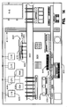
- Fig. 14 portrays another embodiment of the information handling system of the invention in which heat spreaders are connected to ceramic and semiconductor surfaces using flexible epoxies and silicon rubber.
- enclosure 600 contains vertical circuit boards 602, 603 and horizontal mother board 604.
- the information handling system includes modules 606 defining a CPU, RAM modules 607, ROM modules 608, and I/O processor modules 609 on circuit board 604. Alternately, one or more of such modules may be on the other circuit boards 602, 603.
- Bus 610 connects all the circuit boards of the information handling system together.
- a power supply 612 provides DC power to the mother board which supplies the power to the other board through bus 610.
- Module 620 includes a ceramic or preferably organic wiring substrate 622 connected to circuit board 602 using eutectic solder joints 624. Hole drilled heat sink 626 is connected to encapsulated flip chips 628 by silicon adhesive 630. Pin heat sink 640 is connected to encapsulated flip chip 642 by flexible-epoxy 644. Ceramic column grid array CCGA module 660 includes a ceramic substrate 662 with bottom pads to which columns 664 of high melting temperature solder are welded or soldered with eutectic solder. An encapsulated flip chip 666 is surrounded by a conformal coating and a layer of silicon rubber adhesive 668 connects between the flip chip and a heat sink 670.
Landscapes
- Cooling Or The Like Of Semiconductors Or Solid State Devices (AREA)
- Wire Bonding (AREA)
- Die Bonding (AREA)
Applications Claiming Priority (2)
| Application Number | Priority Date | Filing Date | Title |
|---|---|---|---|
| US672875 | 1991-03-20 | ||
| US08/672,875 US5847929A (en) | 1996-06-28 | 1996-06-28 | Attaching heat sinks directly to flip chips and ceramic chip carriers |
Publications (2)
| Publication Number | Publication Date |
|---|---|
| EP0817253A2 true EP0817253A2 (de) | 1998-01-07 |
| EP0817253A3 EP0817253A3 (de) | 1998-12-23 |
Family
ID=24700379
Family Applications (1)
| Application Number | Title | Priority Date | Filing Date |
|---|---|---|---|
| EP97303096A Withdrawn EP0817253A3 (de) | 1996-06-28 | 1997-05-06 | Befestigung von Kühlkörpern direkt auf Flipchips und Keramik-Chipträgern |
Country Status (5)
| Country | Link |
|---|---|
| US (3) | US5847929A (de) |
| EP (1) | EP0817253A3 (de) |
| JP (1) | JP3201975B2 (de) |
| KR (1) | KR100268205B1 (de) |
| TW (1) | TW380360B (de) |
Cited By (1)
| Publication number | Priority date | Publication date | Assignee | Title |
|---|---|---|---|---|
| EP2387071B1 (de) * | 2006-03-23 | 2021-07-21 | CeramTec GmbH | Trägerkörper für Bauelemente oder Schaltungen |
Families Citing this family (180)
| Publication number | Priority date | Publication date | Assignee | Title |
|---|---|---|---|---|
| JP3094069B2 (ja) * | 1993-12-24 | 2000-10-03 | 日本特殊陶業株式会社 | セラミックパッケージ本体の製造方法 |
| US5688716A (en) * | 1994-07-07 | 1997-11-18 | Tessera, Inc. | Fan-out semiconductor chip assembly |
| US6848173B2 (en) * | 1994-07-07 | 2005-02-01 | Tessera, Inc. | Microelectric packages having deformed bonded leads and methods therefor |
| US6002177A (en) * | 1995-12-27 | 1999-12-14 | International Business Machines Corporation | High density integrated circuit packaging with chip stacking and via interconnections |
| US5802707A (en) * | 1996-03-28 | 1998-09-08 | Intel Corporation | Controlled bondline thickness attachment mechanism |
| US5847929A (en) | 1996-06-28 | 1998-12-08 | International Business Machines Corporation | Attaching heat sinks directly to flip chips and ceramic chip carriers |
| US5786635A (en) * | 1996-12-16 | 1998-07-28 | International Business Machines Corporation | Electronic package with compressible heatsink structure |
| US6551857B2 (en) | 1997-04-04 | 2003-04-22 | Elm Technology Corporation | Three dimensional structure integrated circuits |
| US6403882B1 (en) * | 1997-06-30 | 2002-06-11 | International Business Machines Corporation | Protective cover plate for flip chip assembly backside |
| KR100320983B1 (ko) * | 1997-08-22 | 2002-06-20 | 포만 제프리 엘 | 칩조립체및직접적인개방열전도성경로의제공방법 |
| US6740960B1 (en) * | 1997-10-31 | 2004-05-25 | Micron Technology, Inc. | Semiconductor package including flex circuit, interconnects and dense array external contacts |
| US6539286B1 (en) * | 1998-01-26 | 2003-03-25 | Micron Technology, Inc. | Fluid level sensor |
| US6114190A (en) * | 1998-04-14 | 2000-09-05 | Micron Technology, Inc. | Method of forming heat sink and semiconductor chip assemblies |
| TW366548B (en) * | 1998-04-18 | 1999-08-11 | United Microelectronics Corp | Trench bump block and the application of the same |
| JP3147087B2 (ja) * | 1998-06-17 | 2001-03-19 | 日本電気株式会社 | 積層型半導体装置放熱構造 |
| US6409859B1 (en) * | 1998-06-30 | 2002-06-25 | Amerasia International Technology, Inc. | Method of making a laminated adhesive lid, as for an Electronic device |
| US6111314A (en) * | 1998-08-26 | 2000-08-29 | International Business Machines Corporation | Thermal cap with embedded particles |
| US6117797A (en) | 1998-09-03 | 2000-09-12 | Micron Technology, Inc. | Attachment method for heat sinks and devices involving removal of misplaced encapsulant |
| US6092926A (en) * | 1998-09-17 | 2000-07-25 | International Business Machines Corporation | Thermal monitoring system for semiconductor devices |
| US6255140B1 (en) * | 1998-10-19 | 2001-07-03 | Industrial Technology Research Institute | Flip chip chip-scale package |
| US6168976B1 (en) * | 1999-01-06 | 2001-01-02 | Intel Corporation | Socketable BGA package |
| US6197619B1 (en) * | 1999-01-28 | 2001-03-06 | International Business Machines Corporation | Method for reinforcing a semiconductor device to prevent cracking |
| US6531771B1 (en) | 1999-04-20 | 2003-03-11 | Tyco Electronics Corporation | Dissipation of heat from a circuit board having bare silicon chips mounted thereon |
| US6162663A (en) * | 1999-04-20 | 2000-12-19 | Schoenstein; Paul G. | Dissipation of heat from a circuit board having bare silicon chips mounted thereon |
| DE19920593B4 (de) * | 1999-05-05 | 2006-07-13 | Assa Abloy Identification Technology Group Ab | Chipträger für ein Chipmodul und Verfahren zur Herstellung des Chipmoduls |
| US6219238B1 (en) | 1999-05-10 | 2001-04-17 | International Business Machines Corporation | Structure for removably attaching a heat sink to surface mount packages |
| US6717819B1 (en) * | 1999-06-01 | 2004-04-06 | Amerasia International Technology, Inc. | Solderable flexible adhesive interposer as for an electronic package, and method for making same |
| JP3277996B2 (ja) * | 1999-06-07 | 2002-04-22 | 日本電気株式会社 | 回路装置、その製造方法 |
| US6387732B1 (en) * | 1999-06-18 | 2002-05-14 | Micron Technology, Inc. | Methods of attaching a semiconductor chip to a leadframe with a footprint of about the same size as the chip and packages formed thereby |
| US6369452B1 (en) | 1999-07-27 | 2002-04-09 | International Business Machines Corporation | Cap attach surface modification for improved adhesion |
| US6255143B1 (en) * | 1999-08-04 | 2001-07-03 | St. Assembly Test Services Pte Ltd. | Flip chip thermally enhanced ball grid array |
| JP3414342B2 (ja) * | 1999-11-25 | 2003-06-09 | 日本電気株式会社 | 集積回路チップの実装構造および実装方法 |
| US6338196B1 (en) | 1999-12-15 | 2002-01-15 | Auer Precision Company, Inc | Method of forming heat sinks having fully anodized surfaces |
| JP3471690B2 (ja) * | 1999-12-16 | 2003-12-02 | 沖電気工業株式会社 | 半導体素子の実装方法 |
| WO2001047013A1 (en) * | 1999-12-21 | 2001-06-28 | Advanced Micro Devices, Inc. | Organic packages with solders for reliable flip chip connections |
| US6492202B1 (en) * | 1999-12-28 | 2002-12-10 | Motorola, Inc. | Method of assembling components onto a circuit board |
| US6982192B1 (en) * | 1999-12-30 | 2006-01-03 | Intel Corporation | High performance thermal interface curing process for organic flip chip packages |
| US6229207B1 (en) | 2000-01-13 | 2001-05-08 | Advanced Micro Devices, Inc. | Organic pin grid array flip chip carrier package |
| US6342730B1 (en) * | 2000-01-28 | 2002-01-29 | Advanced Semiconductor Engineering, Inc. | Low-pin-count chip package and manufacturing method thereof |
| EP1122780A3 (de) * | 2000-01-31 | 2004-01-02 | Ngk Insulators, Ltd. | Laminatkühler, Leistungshalbleiter und seine Herstellung |
| JP2001227902A (ja) * | 2000-02-16 | 2001-08-24 | Mitsubishi Electric Corp | 半導体装置 |
| US6763881B1 (en) * | 2000-02-18 | 2004-07-20 | Agilent Technologies, Inc. | Thermally matched gradient heat sink |
| US6396700B1 (en) * | 2000-06-29 | 2002-05-28 | International Business Machines Corporation | Thermal spreader and interface assembly for heat generating component of an electronic device |
| JP2002033411A (ja) * | 2000-07-13 | 2002-01-31 | Nec Corp | ヒートスプレッダ付き半導体装置及びその製造方法 |
| US6403401B1 (en) * | 2000-08-14 | 2002-06-11 | St Assembly Test Services Pte Ltd | Heat spreader hole pin 1 identifier |
| US6490162B2 (en) * | 2000-08-24 | 2002-12-03 | International Rectifier Corporation | Heatsink retainer |
| US6278613B1 (en) | 2000-09-27 | 2001-08-21 | St Assembly Test Services Pte Ltd | Copper pads for heat spreader attach |
| JP3634735B2 (ja) * | 2000-10-05 | 2005-03-30 | 三洋電機株式会社 | 半導体装置および半導体モジュール |
| US6586279B1 (en) * | 2000-11-17 | 2003-07-01 | Sun Microsystems, Inc. | Method of integrating a heat spreader and a semiconductor, and package formed thereby |
| US6644983B2 (en) | 2001-02-09 | 2003-11-11 | International Business Machines Corporation | Contact assembly, connector assembly utilizing same, and electronic assembly |
| TW535936U (en) * | 2001-02-27 | 2003-06-01 | Quanta Comp Inc | Stabilizing sheet of heat sink |
| US6610560B2 (en) * | 2001-05-11 | 2003-08-26 | Siliconware Precision Industries Co., Ltd. | Chip-on-chip based multi-chip module with molded underfill and method of fabricating the same |
| US6765806B1 (en) * | 2001-06-12 | 2004-07-20 | Lsi Logic Corporation | Composition with EMC shielding characteristics |
| US6914786B1 (en) * | 2001-06-14 | 2005-07-05 | Lsi Logic Corporation | Converter device |
| US6683375B2 (en) * | 2001-06-15 | 2004-01-27 | Fairchild Semiconductor Corporation | Semiconductor die including conductive columns |
| US7215022B2 (en) * | 2001-06-21 | 2007-05-08 | Ati Technologies Inc. | Multi-die module |
| US7015072B2 (en) | 2001-07-11 | 2006-03-21 | Asat Limited | Method of manufacturing an enhanced thermal dissipation integrated circuit package |
| US6734552B2 (en) | 2001-07-11 | 2004-05-11 | Asat Limited | Enhanced thermal dissipation integrated circuit package |
| JP3580293B2 (ja) * | 2002-03-26 | 2004-10-20 | 株式会社デンソー | 半導体装置の製造方法 |
| US7145254B2 (en) * | 2001-07-26 | 2006-12-05 | Denso Corporation | Transfer-molded power device and method for manufacturing transfer-molded power device |
| US6563198B1 (en) | 2001-08-01 | 2003-05-13 | Lsi Logic Corporation | Adhesive pad having EMC shielding characteristics |
| US6458626B1 (en) * | 2001-08-03 | 2002-10-01 | Siliconware Precision Industries Co., Ltd. | Fabricating method for semiconductor package |
| US7126218B1 (en) * | 2001-08-07 | 2006-10-24 | Amkor Technology, Inc. | Embedded heat spreader ball grid array |
| US6979894B1 (en) * | 2001-09-27 | 2005-12-27 | Marvell International Ltd. | Integrated chip package having intermediate substrate |
| US6748350B2 (en) * | 2001-09-27 | 2004-06-08 | Intel Corporation | Method to compensate for stress between heat spreader and thermal interface material |
| US6627978B2 (en) * | 2001-09-28 | 2003-09-30 | Intel Corporation | Chip package enabling increased input/output density |
| US6737750B1 (en) | 2001-12-07 | 2004-05-18 | Amkor Technology, Inc. | Structures for improving heat dissipation in stacked semiconductor packages |
| US6661102B1 (en) * | 2002-01-18 | 2003-12-09 | Advance Micro Devices, Inc. | Semiconductor packaging apparatus for controlling die attach fillet height to reduce die shear stress |
| US6804118B2 (en) * | 2002-03-15 | 2004-10-12 | Delphi Technologies, Inc. | Thermal dissipation assembly for electronic components |
| US20030178719A1 (en) * | 2002-03-22 | 2003-09-25 | Combs Edward G. | Enhanced thermal dissipation integrated circuit package and method of manufacturing enhanced thermal dissipation integrated circuit package |
| US6534859B1 (en) * | 2002-04-05 | 2003-03-18 | St. Assembly Test Services Ltd. | Semiconductor package having heat sink attached to pre-molded cavities and method for creating the package |
| US6706563B2 (en) | 2002-04-10 | 2004-03-16 | St Assembly Test Services Pte Ltd | Heat spreader interconnect methodology for thermally enhanced PBGA packages |
| US6829264B2 (en) * | 2002-05-10 | 2004-12-07 | Intel Corporation | Laser frequency aging compensation |
| US6853068B1 (en) | 2002-05-22 | 2005-02-08 | Volterra Semiconductor Corporation | Heatsinking and packaging of integrated circuit chips |
| US6835592B2 (en) * | 2002-05-24 | 2004-12-28 | Micron Technology, Inc. | Methods for molding a semiconductor die package with enhanced thermal conductivity |
| JP3679786B2 (ja) * | 2002-06-25 | 2005-08-03 | 松下電器産業株式会社 | 半導体装置の製造方法 |
| CN1681648A (zh) * | 2002-07-15 | 2005-10-12 | 霍尼韦尔国际公司 | 热互连和界面系统,其制备方法及其应用 |
| US6667191B1 (en) * | 2002-08-05 | 2003-12-23 | Asat Ltd. | Chip scale integrated circuit package |
| WO2004015764A2 (en) | 2002-08-08 | 2004-02-19 | Leedy Glenn J | Vertical system integration |
| US20040072927A1 (en) * | 2002-10-14 | 2004-04-15 | Hachikian Zakar Raffi | Two-part epoxy adhesives with improved flexibility and process for making and using same |
| US6775140B2 (en) * | 2002-10-21 | 2004-08-10 | St Assembly Test Services Ltd. | Heat spreaders, heat spreader packages, and fabrication methods for use with flip chip semiconductor devices |
| US6778398B2 (en) * | 2002-10-24 | 2004-08-17 | Koninklijke Philips Electronics N.V. | Thermal-conductive substrate package |
| TW200411871A (en) * | 2002-12-30 | 2004-07-01 | Advanced Semiconductor Eng | Thermal-enhance package and manufacturing method thereof |
| TW577153B (en) * | 2002-12-31 | 2004-02-21 | Advanced Semiconductor Eng | Cavity-down MCM package |
| US20040150956A1 (en) * | 2003-01-24 | 2004-08-05 | Robert Conte | Pin fin heat sink for power electronic applications |
| JP2004253736A (ja) * | 2003-02-21 | 2004-09-09 | Ngk Insulators Ltd | ヒートスプレッダモジュール |
| US7170306B2 (en) * | 2003-03-12 | 2007-01-30 | Celerity Research, Inc. | Connecting a probe card and an interposer using a compliant connector |
| US20040177995A1 (en) * | 2003-03-12 | 2004-09-16 | Nexcleon, Inc. | Structures for testing circuits and methods for fabricating the structures |
| US6924654B2 (en) * | 2003-03-12 | 2005-08-02 | Celerity Research, Inc. | Structures for testing circuits and methods for fabricating the structures |
| US6882535B2 (en) * | 2003-03-31 | 2005-04-19 | Intel Corporation | Integrated heat spreader with downset edge, and method of making same |
| TW576549U (en) * | 2003-04-04 | 2004-02-11 | Advanced Semiconductor Eng | Multi-chip package combining wire-bonding and flip-chip configuration |
| US7126228B2 (en) * | 2003-04-23 | 2006-10-24 | Micron Technology, Inc. | Apparatus for processing semiconductor devices in a singulated form |
| US7004243B1 (en) * | 2003-07-22 | 2006-02-28 | Unisys Corporation | Method of extending the operational period of a heat-exchanger in a chip tester |
| KR100517075B1 (ko) * | 2003-08-11 | 2005-09-26 | 삼성전자주식회사 | 반도체 소자 제조 방법 |
| US20060289979A1 (en) * | 2003-08-26 | 2006-12-28 | God Ralf | Bridge modules for smart labels |
| US7214442B2 (en) * | 2003-12-02 | 2007-05-08 | Los Alamos National Security, Llc | High specific power, direct methanol fuel cell stack |
| US20050127484A1 (en) * | 2003-12-16 | 2005-06-16 | Texas Instruments Incorporated | Die extender for protecting an integrated circuit die on a flip chip package |
| US20060035413A1 (en) * | 2004-01-13 | 2006-02-16 | Cookson Electronics, Inc. | Thermal protection for electronic components during processing |
| US20050151555A1 (en) * | 2004-01-13 | 2005-07-14 | Cookson Electronics, Inc. | Cooling devices and methods of using them |
| DE602004010061T2 (de) * | 2004-03-09 | 2008-09-11 | Infineon Technologies Ag | Hochzuverlässige, kostengünstige und thermisch verbesserte Halbleiterchip-Befestigungstechnologie mit AuSn |
| US20050258536A1 (en) * | 2004-05-21 | 2005-11-24 | Taiwan Semiconductor Manufacturing Co., Ltd. | Chip heat sink device and method |
| US7362580B2 (en) * | 2004-06-18 | 2008-04-22 | Intel Corporation | Electronic assembly having an indium wetting layer on a thermally conductive body |
| KR20060018453A (ko) * | 2004-08-24 | 2006-03-02 | 삼성전자주식회사 | 히트 싱크를 갖는 반도체 소자 |
| US7387478B2 (en) * | 2004-08-27 | 2008-06-17 | Ford Motor Company | Machining system with integrated chip hopper |
| US20060065387A1 (en) * | 2004-09-28 | 2006-03-30 | General Electric Company | Electronic assemblies and methods of making the same |
| TWI336022B (en) * | 2004-10-29 | 2011-01-11 | Altus Technology Inc | Digital still camera lens module |
| US20060163707A1 (en) * | 2005-01-21 | 2006-07-27 | Motorola, Inc. | Method and apparatus for reducing stresses applied to bonded interconnects between substrates |
| JP2006210410A (ja) * | 2005-01-25 | 2006-08-10 | Toshiba Corp | 半導体装置 |
| US7743963B1 (en) | 2005-03-01 | 2010-06-29 | Amerasia International Technology, Inc. | Solderable lid or cover for an electronic circuit |
| TWI253154B (en) * | 2005-05-06 | 2006-04-11 | Neobulb Technologies Inc | Integrated circuit packaging and method of making the same |
| DE102005023949B4 (de) * | 2005-05-20 | 2019-07-18 | Infineon Technologies Ag | Verfahren zur Herstellung eines Nutzens aus einer Verbundplatte mit Halbleiterchips und einer Kunststoffgehäusemasse und ein Verfahren zur Herstellung von Halbleiterbauteilen mittels eines Nutzens |
| JP5042017B2 (ja) * | 2005-05-27 | 2012-10-03 | 株式会社Neomaxマテリアル | 銀被覆ボールおよびその製造方法 |
| US7566591B2 (en) * | 2005-08-22 | 2009-07-28 | Broadcom Corporation | Method and system for secure heat sink attachment on semiconductor devices with macroscopic uneven surface features |
| US7830021B1 (en) * | 2005-09-06 | 2010-11-09 | Rockwell Collins, Inc. | Tamper resistant packaging with transient liquid phase bonding |
| US7408243B2 (en) * | 2005-12-14 | 2008-08-05 | Honeywell International Inc. | High temperature package flip-chip bonding to ceramic |
| JP5165207B2 (ja) | 2006-03-29 | 2013-03-21 | オンセミコンダクター・トレーディング・リミテッド | 半導体装置の製造方法 |
| US7990727B1 (en) * | 2006-04-03 | 2011-08-02 | Aprolase Development Co., Llc | Ball grid array stack |
| US9386327B2 (en) | 2006-05-24 | 2016-07-05 | Time Warner Cable Enterprises Llc | Secondary content insertion apparatus and methods |
| US8280982B2 (en) | 2006-05-24 | 2012-10-02 | Time Warner Cable Inc. | Personal content server apparatus and methods |
| US8024762B2 (en) | 2006-06-13 | 2011-09-20 | Time Warner Cable Inc. | Methods and apparatus for providing virtual content over a network |
| US8124460B2 (en) * | 2006-07-17 | 2012-02-28 | Stats Chippac Ltd. | Integrated circuit package system employing an exposed thermally conductive coating |
| US20080026181A1 (en) * | 2006-07-25 | 2008-01-31 | Ravi Rastogi | Synergistically-modified surfaces and surface profiles for use with thermal interconnect and interface materials, methods of production and uses thereof |
| US7498908B2 (en) * | 2006-08-04 | 2009-03-03 | Advanced Energy Industries, Inc | High-power PIN diode switch |
| JP2008078205A (ja) * | 2006-09-19 | 2008-04-03 | Fujitsu Ltd | 基板組立体及びその製造方法、電子部品組立体及びその製造方法、電子装置 |
| US7589971B2 (en) * | 2006-10-10 | 2009-09-15 | Deere & Company | Reconfigurable heat sink assembly |
| KR100874910B1 (ko) * | 2006-10-30 | 2008-12-19 | 삼성전자주식회사 | 수직형 열방출 통로를 갖는 적층형 반도체 패키지 및 그제조방법 |
| US8181206B2 (en) | 2007-02-28 | 2012-05-15 | Time Warner Cable Inc. | Personal content server apparatus and methods |
| US7468886B2 (en) * | 2007-03-05 | 2008-12-23 | International Business Machines Corporation | Method and structure to improve thermal dissipation from semiconductor devices |
| US9503691B2 (en) | 2008-02-19 | 2016-11-22 | Time Warner Cable Enterprises Llc | Methods and apparatus for enhanced advertising and promotional delivery in a network |
| TW200939869A (en) * | 2008-03-05 | 2009-09-16 | Harvatek Corp | An LED chip package structure with a high-efficiency heat-dissipating substrate and packaging method thereof |
| JP4638923B2 (ja) * | 2008-03-31 | 2011-02-23 | 日立オートモティブシステムズ株式会社 | 制御装置 |
| WO2009131913A2 (en) * | 2008-04-21 | 2009-10-29 | Honeywell International Inc. | Thermal interconnect and interface materials, methods of production and uses thereof |
| US20100096658A1 (en) * | 2008-10-20 | 2010-04-22 | Wu Ming-Chang | Structure of Light Emitting Diode |
| US8202765B2 (en) | 2009-01-22 | 2012-06-19 | International Business Machines Corporation | Achieving mechanical and thermal stability in a multi-chip package |
| TW201032300A (en) * | 2009-02-27 | 2010-09-01 | Advanced Semiconductor Eng | Chip scale package and method of fabricating the same |
| JP5532744B2 (ja) * | 2009-08-20 | 2014-06-25 | 富士通株式会社 | マルチチップモジュール及びマルチチップモジュールの製造方法 |
| US8299482B2 (en) * | 2009-10-05 | 2012-10-30 | Intellectual Discovery Co., Ltd. | Light emitter |
| US8362609B1 (en) | 2009-10-27 | 2013-01-29 | Xilinx, Inc. | Integrated circuit package and method of forming an integrated circuit package |
| US8237293B2 (en) * | 2009-11-25 | 2012-08-07 | Freescale Semiconductor, Inc. | Semiconductor package with protective tape |
| US20110139364A1 (en) * | 2009-12-16 | 2011-06-16 | Matienzo Luis J | Chemical modification of chromate conversion coated aluminum work pieces |
| JP5035356B2 (ja) * | 2010-01-26 | 2012-09-26 | 株式会社デンソー | 樹脂封止型電子装置およびその製造方法 |
| US8810028B1 (en) | 2010-06-30 | 2014-08-19 | Xilinx, Inc. | Integrated circuit packaging devices and methods |
| JP5367656B2 (ja) * | 2010-07-29 | 2013-12-11 | 日東電工株式会社 | フリップチップ型半導体裏面用フィルム及びその用途 |
| CN102956576B (zh) * | 2011-08-29 | 2015-12-02 | 奇鋐科技股份有限公司 | 散热装置及其制造方法 |
| US8872332B2 (en) * | 2012-04-30 | 2014-10-28 | Infineon Technologies Ag | Power module with directly attached thermally conductive structures |
| US8946871B2 (en) * | 2012-11-07 | 2015-02-03 | Lsi Corporation | Thermal improvement of integrated circuit packages |
| US9470715B2 (en) | 2013-01-11 | 2016-10-18 | Mpi Corporation | Probe head |
| TWI453420B (zh) * | 2013-01-11 | 2014-09-21 | Mpi Corp | 孔板 |
| JP5930980B2 (ja) * | 2013-02-06 | 2016-06-08 | 三菱電機株式会社 | 半導体装置およびその製造方法 |
| US20140282786A1 (en) | 2013-03-12 | 2014-09-18 | Time Warner Cable Enterprises Llc | Methods and apparatus for providing and uploading content to personalized network storage |
| KR101625264B1 (ko) * | 2013-05-30 | 2016-05-27 | 제일모직주식회사 | 방열 접착 필름, 이를 포함하는 반도체 장치 및 상기 장치의 제조 방법 |
| KR101827186B1 (ko) * | 2013-09-04 | 2018-02-07 | 미쓰비시덴키 가부시키가이샤 | 반도체 모듈 및 인버터 장치 |
| JP2015082576A (ja) * | 2013-10-22 | 2015-04-27 | 富士通株式会社 | 電子装置、電子機器及び電子装置の製造方法 |
| US9252121B2 (en) * | 2014-01-23 | 2016-02-02 | International Business Machines Corporation | Thermal interface material on package |
| US9693488B2 (en) | 2015-02-13 | 2017-06-27 | Deere & Company | Electronic assembly with one or more heat sinks |
| US9860987B2 (en) | 2015-02-13 | 2018-01-02 | Deere & Company | Electronic assembly with one or more heat sinks |
| FR3036918B1 (fr) * | 2015-05-29 | 2018-08-10 | Thales | Carte electronique et procede de fabrication associe |
| US9603283B1 (en) | 2015-10-09 | 2017-03-21 | Raytheon Company | Electronic module with free-formed self-supported vertical interconnects |
| DE102015118245B4 (de) * | 2015-10-26 | 2024-10-10 | Infineon Technologies Austria Ag | Elektronische Komponente mit einem thermischen Schnittstellenmaterial, Herstellungsverfahren für eine elektronische Komponente, Wärmeabfuhrkörper mit einem thermischen Schnittstellenmaterial und thermisches Schnittstellenmaterial |
| US10283476B2 (en) * | 2017-03-15 | 2019-05-07 | Immunolight, Llc. | Adhesive bonding composition and electronic components prepared from the same |
| US10608158B2 (en) | 2017-09-29 | 2020-03-31 | International Business Machines Corporation | Two-component bump metallization |
| US10727391B2 (en) | 2017-09-29 | 2020-07-28 | International Business Machines Corporation | Bump bonded cryogenic chip carrier |
| US10721840B2 (en) | 2017-10-11 | 2020-07-21 | DISH Technologies L.L.C. | Heat spreader assembly |
| CN111095521B (zh) * | 2017-10-24 | 2023-03-28 | 日本碍子株式会社 | 晶片载置台及其制法 |
| KR102420589B1 (ko) | 2017-12-04 | 2022-07-13 | 삼성전자주식회사 | 히트 싱크를 가지는 반도체 패키지 |
| EP3595002A1 (de) | 2018-07-12 | 2020-01-15 | Heraeus Deutschland GmbH & Co KG | Metall-keramik-substrat mit einer zur direkten kühlung geformten folie als substratunterseite |
| US11348854B2 (en) * | 2019-05-17 | 2022-05-31 | Advanced Semiconductor Engineering, Inc. | Semiconductor package structure and method for manufacturing the same |
| CN110429070B (zh) * | 2019-07-03 | 2024-05-28 | 无锡市乾野微纳科技有限公司 | 可双面散热的功率元件 |
| US11164804B2 (en) | 2019-07-23 | 2021-11-02 | International Business Machines Corporation | Integrated circuit (IC) device package lid attach utilizing nano particle metallic paste |
| CN113905517B (zh) * | 2020-07-06 | 2023-09-22 | 庆鼎精密电子(淮安)有限公司 | 电路板及其制备方法、背光板 |
| US11876345B2 (en) * | 2020-09-08 | 2024-01-16 | Hewlett Packard Enterprise Development Lp | Thermal management for hybrid lasers |
| US11602454B1 (en) * | 2020-10-13 | 2023-03-14 | Hyper Ice, Inc. | Temperature modulation assembly and a multi-layer retention mechanism for a temperature therapy device |
| US11791270B2 (en) | 2021-05-10 | 2023-10-17 | International Business Machines Corporation | Direct bonded heterogeneous integration silicon bridge |
| US11800687B2 (en) | 2021-08-26 | 2023-10-24 | Dish Network L.L.C. | Heat transfer assembly |
| US12322674B2 (en) | 2022-02-10 | 2025-06-03 | Raytheon Company | Thermal spreader including ringframe and thermal straps for thermal dissipation in space and other applications |
| US12002795B2 (en) | 2022-04-13 | 2024-06-04 | Google Llc | Pluggable CPU modules with vertical power |
| US12308543B2 (en) | 2022-04-18 | 2025-05-20 | Google Llc | Structure for optimal XPU socket compression |
| US12581972B2 (en) * | 2022-06-24 | 2026-03-17 | Intel Corporation | Electrically conductive strips on a side of a memory module |
| CN115621365A (zh) * | 2022-11-04 | 2023-01-17 | 大庆华研环保应用技术研发中心有限公司 | 一种光伏装置制备工艺 |
| EP4716440A1 (de) * | 2023-05-16 | 2026-03-25 | Fujitsu Limited | Laminierte struktur, quantenvorrichtung und verfahren zur herstellung einer laminierten struktur |
Family Cites Families (32)
| Publication number | Priority date | Publication date | Assignee | Title |
|---|---|---|---|---|
| US4000509A (en) * | 1975-03-31 | 1976-12-28 | International Business Machines Corporation | High density air cooled wafer package having improved thermal dissipation |
| US4092697A (en) * | 1976-12-06 | 1978-05-30 | International Business Machines Corporation | Heat transfer mechanism for integrated circuit package |
| US4604644A (en) * | 1985-01-28 | 1986-08-05 | International Business Machines Corporation | Solder interconnection structure for joining semiconductor devices to substrates that have improved fatigue life, and process for making |
| JPS61271319A (ja) * | 1985-05-24 | 1986-12-01 | Shin Etsu Chem Co Ltd | 半導体封止用エポキシ樹脂組成物 |
| US4701842A (en) * | 1985-10-04 | 1987-10-20 | International Business Machines Corporation | Method and apparatus for avoiding excessive delay in a pipelined processor during the execution of a microbranch instruction |
| JPH0777247B2 (ja) * | 1986-09-17 | 1995-08-16 | 富士通株式会社 | 半導体装置の製造方法 |
| US5159535A (en) * | 1987-03-11 | 1992-10-27 | International Business Machines Corporation | Method and apparatus for mounting a flexible film semiconductor chip carrier on a circuitized substrate |
| JPH0617458B2 (ja) * | 1987-03-16 | 1994-03-09 | 信越化学工業株式会社 | エポキシ樹脂組成物 |
| JPH0756887B2 (ja) * | 1988-04-04 | 1995-06-14 | 株式会社日立製作所 | 半導体パッケージ及びそれを用いたコンピュータ |
| DE3813565A1 (de) * | 1988-04-22 | 1989-11-02 | Bosch Gmbh Robert | Elektrischer anschluss von hybridbaugruppen |
| US4914551A (en) * | 1988-07-13 | 1990-04-03 | International Business Machines Corporation | Electronic package with heat spreader member |
| GB2236213A (en) * | 1989-09-09 | 1991-03-27 | Ibm | Integral protective enclosure for an assembly mounted on a flexible printed circuit board |
| US5089440A (en) * | 1990-03-14 | 1992-02-18 | International Business Machines Corporation | Solder interconnection structure and process for making |
| US5050039A (en) * | 1990-06-26 | 1991-09-17 | Digital Equipment Corporation | Multiple circuit chip mounting and cooling arrangement |
| US5147084A (en) * | 1990-07-18 | 1992-09-15 | International Business Machines Corporation | Interconnection structure and test method |
| US5377077A (en) * | 1990-08-01 | 1994-12-27 | Staktek Corporation | Ultra high density integrated circuit packages method and apparatus |
| US5287247A (en) * | 1990-09-21 | 1994-02-15 | Lsi Logic Corporation | Computer system module assembly |
| JPH04257248A (ja) * | 1991-02-12 | 1992-09-11 | Mitsubishi Electric Corp | 混成集積回路装置 |
| US5210941A (en) * | 1991-07-19 | 1993-05-18 | Poly Circuits, Inc. | Method for making circuit board having a metal support |
| US5434750A (en) * | 1992-02-07 | 1995-07-18 | Lsi Logic Corporation | Partially-molded, PCB chip carrier package for certain non-square die shapes |
| US5262927A (en) * | 1992-02-07 | 1993-11-16 | Lsi Logic Corporation | Partially-molded, PCB chip carrier package |
| DE69300506T2 (de) * | 1992-04-06 | 1996-04-04 | Nippon Electric Co | Herstellungsverfahren von mehrlagigen keramischen Substraten. |
| EP0566872A3 (en) * | 1992-04-21 | 1994-05-11 | Motorola Inc | A thermally enhanced semiconductor device and method for making the same |
| US5278724A (en) * | 1992-07-06 | 1994-01-11 | International Business Machines Corporation | Electronic package and method of making same |
| US5367196A (en) * | 1992-09-17 | 1994-11-22 | Olin Corporation | Molded plastic semiconductor package including an aluminum alloy heat spreader |
| US5459352A (en) * | 1993-03-31 | 1995-10-17 | Unisys Corporation | Integrated circuit package having a liquid metal-aluminum/copper joint |
| US5831828A (en) * | 1993-06-03 | 1998-11-03 | International Business Machines Corporation | Flexible circuit board and common heat spreader assembly |
| JPH0758254A (ja) * | 1993-08-19 | 1995-03-03 | Fujitsu Ltd | マルチチップモジュール及びその製造方法 |
| US5591034A (en) * | 1994-02-14 | 1997-01-07 | W. L. Gore & Associates, Inc. | Thermally conductive adhesive interface |
| US5572405A (en) * | 1995-06-07 | 1996-11-05 | International Business Machines Corporation (Ibm) | Thermally enhanced ball grid array package |
| US5729052A (en) * | 1996-06-20 | 1998-03-17 | International Business Machines Corporation | Integrated ULSI heatsink |
| US5847929A (en) * | 1996-06-28 | 1998-12-08 | International Business Machines Corporation | Attaching heat sinks directly to flip chips and ceramic chip carriers |
-
1996
- 1996-06-28 US US08/672,875 patent/US5847929A/en not_active Expired - Fee Related
-
1997
- 1997-01-20 TW TW086100567A patent/TW380360B/zh not_active IP Right Cessation
- 1997-04-25 KR KR1019970015491A patent/KR100268205B1/ko not_active Expired - Fee Related
- 1997-05-06 EP EP97303096A patent/EP0817253A3/de not_active Withdrawn
- 1997-06-23 JP JP16599897A patent/JP3201975B2/ja not_active Expired - Fee Related
-
1998
- 1998-06-10 US US09/094,401 patent/US6069023A/en not_active Expired - Lifetime
-
2000
- 2000-04-11 US US09/546,567 patent/US6251707B1/en not_active Expired - Fee Related
Cited By (1)
| Publication number | Priority date | Publication date | Assignee | Title |
|---|---|---|---|---|
| EP2387071B1 (de) * | 2006-03-23 | 2021-07-21 | CeramTec GmbH | Trägerkörper für Bauelemente oder Schaltungen |
Also Published As
| Publication number | Publication date |
|---|---|
| KR980006192A (ko) | 1998-03-30 |
| US6251707B1 (en) | 2001-06-26 |
| JPH1070141A (ja) | 1998-03-10 |
| TW380360B (en) | 2000-01-21 |
| EP0817253A3 (de) | 1998-12-23 |
| US6069023A (en) | 2000-05-30 |
| JP3201975B2 (ja) | 2001-08-27 |
| US5847929A (en) | 1998-12-08 |
| KR100268205B1 (ko) | 2000-10-16 |
Similar Documents
| Publication | Publication Date | Title |
|---|---|---|
| US6069023A (en) | Attaching heat sinks directly to flip chips and ceramic chip carriers | |
| US5672548A (en) | Method for attaching heat sinks directly to chip carrier modules using flexible-epoxy | |
| CN1085891C (zh) | 芯片载体及使用它的半导体装置 | |
| US6734552B2 (en) | Enhanced thermal dissipation integrated circuit package | |
| US7521794B2 (en) | Intrinsic thermal enhancement for FBGA package | |
| US6927095B2 (en) | Low cost and compliant microelectronic packages for high I/O and fine pitch | |
| US7208819B2 (en) | Power module package having improved heat dissipating capability | |
| US6806567B2 (en) | Chip on board with heat sink attachment and assembly | |
| US7759170B2 (en) | Fabrication method of semiconductor package having heat dissipation device | |
| US20180151461A1 (en) | Stiffener for fan-out wafer level packaging and method of manufacturing | |
| WO2003083956A2 (en) | Enhanced thermal dissipation integrated circuit package and method of manufacturing enhanced thermal dissipation integrated circuit package | |
| US20070040267A1 (en) | Method and system for secure heat sink attachment on semiconductor devices with macroscopic uneven surface features | |
| JPH08500469A (ja) | 多重チップ・モジュールを組み込んだ金属電子パッケージ | |
| US5888849A (en) | Method for fabricating an electronic package | |
| KR960016006B1 (ko) | Tib 기술을 이용한 디바이스의 상호 접속방법 및 장치 | |
| Hashemi et al. | Enabling Technologies for Low‐count Chip Packaging | |
| Gengel et al. | Characterizing Two Metal Tbga | |
| JPH0613485A (ja) | 半導体装置の製造方法 | |
| TH20718A (th) | การติดอุปกรณ์ระบายความร้อนต่อโดยตรงกับโมดูลชิพพาหะโดยใช้อีพ๊อกซี่ยืดหยุ่น | |
| TH17028B (th) | การติดอุปกรณ์ระบายความร้อนต่อโดยตรงกับโมดูลชิพพาหะโดยใช้อีพ๊อกซี่ยืดหยุ่น | |
| HK1118952A1 (en) | Low profile ball grid array (bga) package with exposed die and method of making same | |
| HK1118952B (en) | Low profile ball grid array (bga) package with exposed die and method of making same | |
| JPH03236300A (ja) | 電子部品搭載用基板 |
Legal Events
| Date | Code | Title | Description |
|---|---|---|---|
| PUAI | Public reference made under article 153(3) epc to a published international application that has entered the european phase |
Free format text: ORIGINAL CODE: 0009012 |
|
| AK | Designated contracting states |
Kind code of ref document: A2 Designated state(s): DE FR GB |
|
| PUAL | Search report despatched |
Free format text: ORIGINAL CODE: 0009013 |
|
| AK | Designated contracting states |
Kind code of ref document: A3 Designated state(s): DE FR GB |
|
| 17P | Request for examination filed |
Effective date: 19990617 |
|
| STAA | Information on the status of an ep patent application or granted ep patent |
Free format text: STATUS: THE APPLICATION IS DEEMED TO BE WITHDRAWN |
|
| 18D | Application deemed to be withdrawn |
Effective date: 20080105 |