EP0819336B1 - Source d'alimentation a haute tension possedant plusieurs generateurs de haute tension - Google Patents
Source d'alimentation a haute tension possedant plusieurs generateurs de haute tension Download PDFInfo
- Publication number
- EP0819336B1 EP0819336B1 EP96912581A EP96912581A EP0819336B1 EP 0819336 B1 EP0819336 B1 EP 0819336B1 EP 96912581 A EP96912581 A EP 96912581A EP 96912581 A EP96912581 A EP 96912581A EP 0819336 B1 EP0819336 B1 EP 0819336B1
- Authority
- EP
- European Patent Office
- Prior art keywords
- voltage
- generator
- power supply
- load
- high voltage
- Prior art date
- Legal status (The legal status is an assumption and is not a legal conclusion. Google has not performed a legal analysis and makes no representation as to the accuracy of the status listed.)
- Expired - Lifetime
Links
Images

Classifications
-
- H—ELECTRICITY
- H05—ELECTRIC TECHNIQUES NOT OTHERWISE PROVIDED FOR
- H05G—X-RAY TECHNIQUE
- H05G1/00—X-ray apparatus involving X-ray tubes; Circuits therefor
- H05G1/08—Electrical details
- H05G1/26—Measuring, controlling or protecting
- H05G1/30—Controlling
- H05G1/32—Supply voltage of the X-ray apparatus or tube
-
- B—PERFORMING OPERATIONS; TRANSPORTING
- B03—SEPARATION OF SOLID MATERIALS USING LIQUIDS OR USING PNEUMATIC TABLES OR JIGS; MAGNETIC OR ELECTROSTATIC SEPARATION OF SOLID MATERIALS FROM SOLID MATERIALS OR FLUIDS; SEPARATION BY HIGH-VOLTAGE ELECTRIC FIELDS
- B03C—MAGNETIC OR ELECTROSTATIC SEPARATION OF SOLID MATERIALS FROM SOLID MATERIALS OR FLUIDS; SEPARATION BY HIGH-VOLTAGE ELECTRIC FIELDS
- B03C3/00—Separating dispersed particles from gases or vapour, e.g. air, by electrostatic effect
- B03C3/34—Constructional details or accessories or operation thereof
- B03C3/66—Applications of electricity supply techniques
- B03C3/68—Control systems therefor
-
- H—ELECTRICITY
- H02—GENERATION; CONVERSION OR DISTRIBUTION OF ELECTRIC POWER
- H02M—APPARATUS FOR CONVERSION BETWEEN AC AND AC, BETWEEN AC AND DC, OR BETWEEN DC AND DC, AND FOR USE WITH MAINS OR SIMILAR POWER SUPPLY SYSTEMS; CONVERSION OF DC OR AC INPUT POWER INTO SURGE OUTPUT POWER; CONTROL OR REGULATION THEREOF
- H02M3/00—Conversion of DC power input into DC power output
- H02M3/22—Conversion of DC power input into DC power output with intermediate conversion into AC
- H02M3/24—Conversion of DC power input into DC power output with intermediate conversion into AC by static converters
- H02M3/28—Conversion of DC power input into DC power output with intermediate conversion into AC by static converters using discharge tubes with control electrode or semiconductor devices with control electrode to produce the intermediate AC
-
- H—ELECTRICITY
- H02—GENERATION; CONVERSION OR DISTRIBUTION OF ELECTRIC POWER
- H02M—APPARATUS FOR CONVERSION BETWEEN AC AND AC, BETWEEN AC AND DC, OR BETWEEN DC AND DC, AND FOR USE WITH MAINS OR SIMILAR POWER SUPPLY SYSTEMS; CONVERSION OF DC OR AC INPUT POWER INTO SURGE OUTPUT POWER; CONTROL OR REGULATION THEREOF
- H02M7/00—Conversion of AC power input into DC power output; Conversion of DC power input into AC power output
- H02M7/02—Conversion of AC power input into DC power output without possibility of reversal
- H02M7/04—Conversion of AC power input into DC power output without possibility of reversal by static converters
- H02M7/06—Conversion of AC power input into DC power output without possibility of reversal by static converters using discharge tubes without control electrode or semiconductor devices without control electrode
- H02M7/10—Conversion of AC power input into DC power output without possibility of reversal by static converters using discharge tubes without control electrode or semiconductor devices without control electrode arranged for operation in series, e.g. for multiplication of voltage
-
- H—ELECTRICITY
- H05—ELECTRIC TECHNIQUES NOT OTHERWISE PROVIDED FOR
- H05G—X-RAY TECHNIQUE
- H05G1/00—X-ray apparatus involving X-ray tubes; Circuits therefor
- H05G1/08—Electrical details
- H05G1/10—Power supply arrangements for feeding the X-ray tube
-
- H—ELECTRICITY
- H05—ELECTRIC TECHNIQUES NOT OTHERWISE PROVIDED FOR
- H05G—X-RAY TECHNIQUE
- H05G1/00—X-ray apparatus involving X-ray tubes; Circuits therefor
- H05G1/08—Electrical details
- H05G1/10—Power supply arrangements for feeding the X-ray tube
- H05G1/20—Power supply arrangements for feeding the X-ray tube with high-frequency AC; with pulse trains
-
- H—ELECTRICITY
- H05—ELECTRIC TECHNIQUES NOT OTHERWISE PROVIDED FOR
- H05G—X-RAY TECHNIQUE
- H05G1/00—X-ray apparatus involving X-ray tubes; Circuits therefor
- H05G1/08—Electrical details
- H05G1/26—Measuring, controlling or protecting
- H05G1/30—Controlling
- H05G1/34—Anode current, heater current or heater voltage of X-ray tube
Definitions
- the present invention relates generally to high voltage power supplies and, in particular, to a high voltage power supply for generating a controlled current in a load having varying inductive and capacitive components.
- High voltage power supplies often are used in applications where a load connected to the power supply includes a significant inductive or capacitive component.
- inductive components comprise a major component of the load.
- electrostatic precipitators contain electrode arrays connected to a high voltage power supply via high voltage cables and buses. The array, the cables, and the buses all contribute to the overall inductive value of the system. Even in applications that do not contain large inductive components, elements of the system may have non-negligible inductive values.
- a load connected to a high voltage power supply may be connected to the power supply by a high voltage cable having an inherent inductance. As a general rule, therefore, all high-power electrical circuits can be modeled with resistive, inductive, and capacitive components.
- a common approach is to convert a DC voltage to a high frequency alternating current (AC) square wave voltage with an inverter, step-up the square wave voltage using a high voltage transformer, and rectify the stepped-up output of the transformer to produce an approximately DC output voltage.
- AC alternating current
- a drawback to this generation method is that it does not allow simple control of the magnitude and waveform of the current generated in the transformer and in the load.
- the magnitude of the current in the load is affected by two changing voltages. First, fluctuations in the primary DC voltage source can cause the amplitude of the AC square wave voltage from the inverter to vary.
- V gen the magnitude of the output voltage generated by the high voltage power supply
- V c the voltage across the capacitive components in the load
- U.S. Patent No. 3,818,307 discloses a power supply that consists of a number of serially connected converters 15-18 (Figure 1) that are designed to supply adequate power to a set of serially connected loads while maintaining a suitable balance among the converters.
- the output voltage requirements of a converter vary considerably, so each converter is provided with one to five power stages 43-47 ( Figure 3).
- the inverters of the power stages 43-47 are driven by a fixed frequency oscillator 57, which provides a 20 KHz timing signal.
- the width of each half-cycle effective to supply power through the inverters is controlled by a pulsewidth modulator 62 driven by the feedback regulator circuitry.
- the power supply as a whole functions so that when the converters 15-18 reach a high current limit, they are put into a substantially constant current mode of regulation, and when they reach a high voltage limit, they are put into a substantially constant voltage mode of regulation.
- the regulating modes of the disclosed power supply are put into effect only when a high current or voltage limit is exceeded. Therefore, the converters are not designed to repetitively cycle through various modes in synchronicity with the 20 KHz timing cycle. It is an object of the present invention to create a power supply wherein during each repetition of a timing signal the power supply cycles through distinct modes of operation that operate to produce the desired output voltage of the power supply.
- a high voltage power supply having a plurality of high voltage generators that may be divided into three groups, hereinafter referred to as Groups I, II, and III.
- Each of the high voltage generators comprises a pulsewidth-modulated (PWM) inverter, a high voltage transformer, and a high voltage full bridge rectifier.
- PWM pulsewidth-modulated
- the PWM inverter generates a high frequency AC voltage that is stepped-up by the transformer and rectified by the rectifier.
- the output voltage (hereinafter V gen ) generated by the power supply is equivalent to the sum of the output voltages from each of the three groups of high voltage generators.
- the output voltage may be applied to a load having varying inductive, capacitive, and resistive elements.
- a voltage (hereinafter V c ) is produced in the load across the capacitive components.
- Each of the groups of high voltage generators contributes a different component to the output voltage produced by the power supply.
- the power supply cycles through two modes of operation to maintain a desired current in the load.
- Groups I, II, and III of the high voltage generators collectively provide an output voltage that exceeds the voltage across the capacitive components in the load.
- Group I generates a tracking voltage (V 1 ) that decreases as the current rises in the load
- Group II generates a base voltage (V 2 ) approximating the voltage across the load
- Group III generates an accelerator voltage (V 3 ) at a level that ensures that the sum of the three voltages exceeds the voltage across the load (i.e., V 1 + V 2 + V 3 > V c ).
- V 1 tracking voltage
- V 2 base voltage
- V 3 accelerator voltage
- Operation in the tracking mode begins when the current in the load reaches a desired level.
- Groups I and II of the high voltage generators operate to collectively provide an output voltage that is equal to the voltage across the capacitive components in the load.
- the Group II component of the output voltage is a substantially constant base voltage (V 2 ), which is equal to or less than the voltage across the load.
- a control circuit is provided to enable or disable additional high voltage generators contained in Group II.
- the high voltage produced by the Group II generators must be capable of producing a broad range of output voltages.
- additional high voltage generators may be turned on-or-off by the control circuit to adjust the output of the power supply.
- the generators are dynamically enabled or removed in response to changes in the voltage across the load. Additional generators may also be enabled when high voltage generators within Group II fail. The failed generators may be dynamically substituted with replacement generators in order to maintain the desired output voltage without substantial interruption. Dynamic replacement of malfunctioning generators enhances the reliability of the high voltage supply.
- the power supply disclosed herein offers several advantages over other high voltage power supplies disclosed in the prior art.
- the present power supply generates a high voltage while controlling the magnitude and waveform of the current in the load and the transformers.
- the current may be controlled despite fluctuations in the difference between the primary voltage and the voltage across the capacitive components in the load. Controlling the current allows the power supply to generate and apply a high voltage having a desired waveform shape. Shaping the waveform voltage is particularly advantageous in state-of-the-art radars and other high voltage applications.
- the number of high voltage generators that are included in each power supply may be selected based on the desired operating range of the power supply. More or less Group II generators may be included to alter the base voltage level applied by the power supply in the driving mode and the tracking mode.
- the use of a modular design therefore increases the applications and flexibility of the power supply.
- high voltage power supplies of the present invention may be connected in parallel with each other to produce a power supply having a desired output power and voltage.
- the parallel connection is possible because the output current from each high voltage power supply is regulated, preventing the power supplies from becoming overloaded.
- Several high voltage power supplies may also be connected in series to create a switched multi-output supply necessary for such applications as traveling wave tubes and x-ray equipment.
- a further advantage of the disclosed power supply is that additional high voltage generators contained in Group II may also be enabled or disabled to compensate for ripples in a rectified AC input voltage.
- DC voltage for the disclosed power supply is provided by rectifying an AC line voltage.
- capacitive filters are required to generate a sufficiently smooth DC voltage to prevent the output from the high voltage power supply from fluctuating.
- the disclosed power supply may enable additional Group II generators as the input DC voltage drops, and disable the Group II generators as the input DC voltage rises, in order to maintain the desired output voltage.
- a still further advantage is that very few energy storage components are included in the power supply design.
- the minimal use of inductors or capacitors allows the high voltage power supply of the present invention to be quickly turned on-or-off.
- the rapid response of the power supply allows it to be used in situations where it would be desirable to quickly turn off the power during the occurrence of a failure condition, such as a short in the load.
- the rapid switching time of the power supply disclosed herein therefore makes it especially suited for applications such as electrostatic precipitators, x-ray equipment, pulse and continuous lasers, and radar systems.
- a high voltage power supply design that is known in the art is represented in the block diagram of FIGURE 1.
- the power supply consists of a primary DC voltage source 20 that provides an unregulated DC voltage to a high voltage generator 22.
- the high voltage generator is connected to a load 24, and contains an inverter 26, a transformer 28, and a rectifier 30 to produce a high voltage for application to the load.
- Inverter 26 converts the unregulated DC voltage from the primary voltage source into a high frequency square wave.
- the high frequency square wave is stepped-up by high voltage transformer 28 and rectified by high voltage rectifier 30.
- the resulting output voltage applied to the load is a fully rectified square wave having a nearly constant DC amplitude.
- Load 24 may be modeled with three components: an inductive component 32, a capacitive component 34, and a resistive component 36.
- V gen the output voltage from the high voltage generator is proportional to the magnitude of the voltage produced by primary voltage source 20. Fluctuations in the primary voltage supply due to instability or voltage ripples directly cause variations in the output voltage V gen .
- V c can change its magnitude due to a change in the voltage drop across the inductive component in the load. The voltage drop across the inductive component may change due to the discharge of energy, for example, during precipitator operation.
- V gen and V c change, the difference between the voltages typically changes, causing a proportional current fluctuation through the inductive component of the load.
- large fluctuations in load currents are to be avoided, as they have the potential to overheat or destroy electric components in the load.
- the object of the present invention is to maintain the magnitude of the current in the load at a desired level independently of any fluctuations in the primary voltage and changes in voltage across the capacitive components.
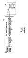
- FIGURE 2 A block diagram of a high voltage power supply 40 constructed according to the present invention is shown in FIGURE 2.
- High voltage power supply 40 consists of three sets of high voltage generators 50 identified as Groups I, II, and III.
- Group I consists of a single high voltage generator 50a
- Group II is made up of eight high voltage generators 50b, 50c,... 50i
- Group III is formed by a single high voltage generator 50j.
- greater or fewer high voltage generators may be included in each group so as to configure the invention for operation at a desired voltage and current level.
- a single-phase AC power source 84 provides power to the high voltage power supply.
- AC power source 84 provides a 120 volt AC voltage at 60Hz.
- the AC power source supplies operating power to an unregulated AC-to-DC rectifier 52 which is connected via lines 100 and 102 to each of the high voltage generators 50b, 50c, ...50j. Connected between lines 100 and 102 is a filter capacitor 88.
- AC power source 84 also provides operating power to a current control circuit 64 that is coupled to high voltage generator 50a.
- rectifier 52 is a full-bridge diode network that produces an unregulated DC voltage. In a realization of such an embodiment, the DC voltage produced by the rectifier is approximately 170 volts.
- Each high voltage generator 50a, 50b,... 50j is comprised of a high voltage inverter 70a, 70b,... 70j, a high voltage transformer 72a, 72b, ... 72j, and a high voltage rectifier 78a, 78b, ...78j.
- the output of each inverter 70a, 70b,... 70j is connected to supply a signal to a corresponding primary winding 74a, 74b,... 74j of transformer 72a, 72b, ... 72j.
- An associated high voltage rectifier 78a, 78b, ... 78j is connected to the secondary winding 76a, 76b,... 76j of each transformer.
- the high voltage generators are connected in a cascode configuration so that the output voltage V gen from the power supply is the sum of the output voltages produced by each of the high voltage generators. That is, each group in the high voltage power supply produces an output voltage that is summed to form V gen .
- the high voltage power supply is connected by a line 80 to a load 24.
- Load 24 may be modeled by an inductive component 32, a capacitive component 34, and a resistive component 36.
- V c When current flows through inductive component 32, a voltage V c is produced across the capacitive component of the load.
- voltage V c will vary as a result of changes in the voltage drop across inductive component 32.
- a change in V c caused by, for example, energy discharge, would typically result in a change in load current.
- the power supply disclosed herein generates a variable output voltage that maintains a nearly constant load current of desired amplitude through the inductive component of the load.
- each of the generator groups is responsible for generating a different component of the output voltage from the power supply.
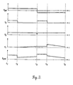
- Representative timing diagrams of the output voltages produced by Groups I, II, and III of the power supply are provided in FIGURE 3, and will be discussed generally below. It will be appreciated that the graphs showing the output voltage from each high voltage generator group are idealized in FIGURE 3. For example, the voltage transitions of the inverters will be dampened somewhat by the load of the high voltage transformer and high voltage rectifier. The waveforms shown in FIGURE 3 are thus to be considered as representative of the shape of the high voltage generator output voltages that produce a desired current (I d ) in the load.
- the specific construction of each high voltage generator group will be subsequently discussed with respect to FIGURES 6, 7, 8, and 9.
- each of the high voltage generators is connected to a timing generator 66.
- the timing generator is provided to synchronously drive each of the inverters in the high voltage generators with a high frequency timing signal.
- the timing signal produced by the timing generator is a square wave voltage having an amplitude of 15 volts and a frequency within the range of 10 to 20 kHz.
- a representative square wave timing signal generated by the timing generator is shown by graph V SW of FIGURE 3.
- each of the generator groups generates a characteristic output voltage beginning with the leading or falling edge of the square wave.
- a square wave timing signal is preferred, those skilled in the art will recognize that the inverters in the high voltage generator may be driven with any repetitive signal. While the discussion below therefore contemplates the use of a periodic square wave timing signal, any non-periodic repetitive timing signal may be used to generate a desired output voltage waveform.
- the Group III high voltage generator 50j generates a periodic rectangular pulse as shown in graph V 3 of FIGURE 3.
- the rectangular pulse begins with the leading edge of the timing signal, and has an amplitude that corresponds to the magnitude of the DC voltage provided by AC-to-DC rectifier 52 and the turns ratio of transformer 72j.
- a current monitor 58 connected between the output of inverter 70j and the primary winding 74j of transformer 72j, senses the current being delivered by the inverter. When the current measured by current monitor 58 corresponds to a desired load current (I d ) through inductive component 32, the inverter of the Group III high voltage generator is switched off. When switched off, the output voltage generated by the Group III generator falls to zero.
- the Group II high voltage generators 50b, 50c,... 50i of FIGURE 2 supply an approximately DC output voltage as shown in graph V 2 of FIGURE 3. That is, each Group II inverter 70b, 70c,... 70i produces a square wave output that is synchronous with the timing signal produced by timing generator 66. The square wave voltage produced by each inverter is stepped-up by the associated transformer and is full wave rectified by the corresponding high voltage rectifier. In the arrangement of FIGURE 2, the output voltage collectively produced by the Group II generators is determined by a control circuit 56 that selectively enables high voltage generators 50b, 50c,... 50i.
- Control circuit 56 receives from a voltage divider network 82 on a line 54 a voltage representative of the voltage V c across the capacitive component of the load.
- the control circuit monitors the voltage across the load, and enables or disables the high voltage generators so that the total voltage generated by the Group II generators is less than or equal to the voltage appearing across the capacitive component of the load.
- the output voltage from the Group II generators may therefore change in incremental steps that correspond to the output voltage produced by each high voltage generator in the group.
- the Group I high voltage generator 50a produces an output voltage V 1 that can range between zero and a value limited by the maximum input voltage being supplied to current control circuit 64.
- the Group I high voltage generator is connected to a current control circuit 64.
- the Group I high voltage generator is a current fed inverter.
- Connected between the current control circuit 64 and the inverter 70a is a current monitor 60.
- Current monitor 60 monitors the amount of current flowing in the inverter. The monitored current is a scaled amount of the current flowing through the secondary winding of the transformer contained in the high voltage generator, and therefore proportional to the current flowing through the power supply and to the load.
- the current control circuit 64 provides additional current to the inverter 70a to increase the voltage generated by the high voltage generator. Conversely, if the current measured by the current monitor 60 indicates a current in the load greater than the desired current I d , the output voltage from high voltage generator 50a is reduced. In this manner, a variable voltage is generated by the Group I high voltage generator in order to track the change in the voltage across the capacitive component and maintain the current in the load at a desired level.
- a representative output voltage generated by the Group I generator is shown in graph V 1 of FIGURE 3.
- each group of high voltage generators produces the above described output voltage
- the power supply cycles through two modes of operation, hereinafter referred to as a driving mode and a tracking mode.
- a driving mode represented by the time interval from t 1 to t 2 in FIGURE 3
- the sum of the Group I, Group II, and Group III generators exceeds the voltage V c measured across the capacitive component of the load.
- the Group I generator produces a high voltage that will dynamically vary during the driving mode.
- the Group II generators produce a substantially constant output voltage comprising a rectified square wave voltage and the Group m generator produces a positive rectangular pulse.
- V 2 and V 3 are selected so that the sum of V 2 and V 3 is a constant voltage that exceeds V c (i.e., V 2 + V 3 > V c ). Since V gen is greater than V c during the driving mode, according to equation (1) the rate of change of current is positive during the period from t 1 to t 2 . The current through the load therefore increases during the driving mode until it reaches a desired level I d . When the current reaches a desired level, current monitor 58 senses the desired current and switches off the Group III inverter 70j. At this point, the power supply enters a tracking mode of operation.
- the power supply When the desired current level is reached, the power supply enters a tracking mode of operation represented by the time interval from t 2 to t 3 in FIGURE 3.
- the voltage V gen generated by the power supply substantially tracks the voltage V c across the capacitive component of the load.
- the output from the high voltage generator in Group III is switched off by the feedback provided by current monitor 58.
- the voltage V gen therefore drops to the level of the sum of the output from the Group I and Group II high voltage generators.
- the Group II generators collectively generate a sum DC voltage less than or equal to the voltage across the load.
- current monitor 60 causes the Group I generator to increase or decrease its output voltage to track voltage changes across the capacitive component in the load.
- Voltage V c may change for a variety of reasons, for example, due to any charging or discharging processes in the load. Absent the invention, any such change in V c would cause a change in load current.
- the power supply disclosed herein maintains voltage V gen at a level substantially equal to V c .
- the current in the load does not appreciably change its magnitude during the tracking mode because the voltage drop across the inductive component of the load is in the ideal sense equal to zero.
- the two-mode voltage generation process repeats during the second half of the period of square wave voltage V SW produced by timing generator 66.
- the polarity of the square wave voltage reverses, and a negative voltage drives the high voltage generators.
- the change in polarity of the voltage driving the high voltage generators causes a momentary drop in the output voltage V gen of the high voltage power supply. This causes V c to exceed V gen , and generates a falling current in the load since, in accordance with equation (1), the change in the current through the inductor is negative.
- the application of the rectified sum of V 1 , V 2, and V 3 causes V gen to exceed V c , and the current to increase through the inductive component in the load.
- the current through the inductor reaches the desired value.
- the power supply of FIGURE 2 begins operation in the tracking mode.
- the output from the high voltage generator in Group III is switched off, and the voltage V gen drops to the level of V 2 , the output from the Group II high voltage generators.
- the high voltage generator in Group I changes its output so that the sum of V 2 and V 1 are equivalent to the voltage V c across the capacitive load.
- Driving mode operation begins again at t 5 in FIGURE 3, i.e., at the end of the negative polarity portion of the square wave timing signal.
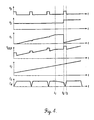
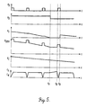
- FIGURES 4 and 5 are timing diagrams showing the effect of a change in the voltage across the capacitive components V c that will result in enabling or disabling a Group II high voltage generator.
- the Group II output voltage V 2 is produced by a plurality of generators 50b, 50c,... 52i.
- the number of Group II generators that are producing a voltage is controlled by control circuit 56, which can selectively enable or disable the output from each of the Group II generators.
- FIGURE 4 represents a case when the voltage V c across the capacitive component in the load is increasing. As the voltage increases, the output voltage V 1 produced by the Group I high voltage generator continues to increase in magnitude to insure that V gen tracks V c .
- the voltage produced by the Group I high voltage generator reaches a maximum dictated by the input voltage to the current control circuit. From time t 1 to time t 2 , the output voltage V 1 remains at a maximum. Because V c continues to increase during this period, however, V c becomes greater than V gen , causing the current I L through the load to drop. Recognizing that the high voltage power supply output voltage can no longer track V c , the control circuit in the power supply enables an additional generator in the Group II high voltage generators. The additional generator in Group II increases the output voltage V 2 produced by the Group II generators, thus increasing the output voltage V gen . By time t 3 , the output voltage produced by Group I and Group II generators is sufficient to again track V c without causing V 1 to saturate. Current I L through the load is therefore returned to the desired amplitude and waveform after time t 3 .
- FIGURE 5 represents a case when the voltage across the capacitive component in the load is decreasing.
- the output voltage V 1 produced by the Group I high voltage generator continues to decrease in magnitude to insure that V gen tracks V c .
- the voltage produced by the Group I high voltage generator reaches a minimum value (substantially equal to zero) wherein it is not producing any component of V gen .
- the output voltage V 1 remains at zero. Because V c continues to decrease during this period, however, V c becomes less than V gen , causing the current I L through the load to increase.
- the control circuit in the power supply disables a generator in the Group II high voltage generators. Eliminating a generator in Group II decreases the output voltage V 2 produced by the Group II generators, thus decreasing the output voltage V gen .
- the output voltage produced by the Group I and Group II generators is sufficient to again track V c without forcing V 1 to zero. Current I L through the load is therefore returned to the desired amplitude and waveform after time t 3 .
- Control circuit 56 can also enable additional Group II generators to replace generators that fail.
- the failed generators may be dynamically substituted with replacement generators in order to maintain the desired output voltage without substantial interruption.
- Several different techniques may be used to detect a failed generator. One technique would be to monitor the output voltage produced by each Group II generator 50b, 50c,... 50i. A sudden and unexpected drop in the output voltage produced by a given generator may be indicative of a failed generator.
- each of the Group II generators may be provided with a fuse. A failure condition causing the fuse to blow could be detected and an additional Group II generator enabled to compensate for the failed generator. Overall, the dynamic replacement of malfunctioning generators under the control of control circuit 56 enhances the reliability of the high voltage supply.
- the Group III high voltage generator is designed to produce a periodic variable-width rectangular pulse that is used as an accelerator voltage during the driving mode of the power supply.
- the Group III generator includes a single high voltage generator 50j.
- the unregulated DC voltage from the AC-to-DC rectifier 52 is directly coupled via lines 100 and 102 to high voltage generator 50j.
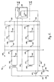
- FIGURE 6 is a circuit diagram of a pulsewidth-modulated (PWM) inverter suitable for use in high voltage generator 50j.
- PWM pulsewidth-modulated
- the PWM inverter 70j is shown schematically as comprising the following primary elements: transformer 148, four power metal-oxide-semiconductor field-effect transistors (MOSFETs) 157, 158, 159, and 160, current transformer 165, resistor 166, and triacs 146 and 147.
- Transistors 157, 158, 159, and 160 are connected in a full-bridge configuration. When one transistor pair, for example transistors 157 and 160, are biased ON (i.e., conducting), the other transistor pair comprising transistors 158 and 159 are switched OFF, allowing current to flow from line 100 through transistor 157 and transformer 165 to terminal 168.
- MOSFETs metal-oxide-semiconductor field-effect transistors
- Terminals 168 and 170 are connected to the primary winding 74j of the high voltage transformer 72j.
- the current flows from terminal 168, through the primary winding of the high voltage transformer, and through terminal 170 and transistor 160 to ground.
- transistors 157 and 160 are switched OFF, and transistors 158 and 159 are biased ON, the current flows through the primary winding 74j in the opposite direction. That is, current flows from line 100 through transistor 159, terminal 170, primary winding 74j, terminal 168, and transistor 158 to ground. Alternately biasing or switching each transistor pair ON or OFF therefore causes current to flow in the primary winding of high voltage transformer 72j in one direction or the other.
- the switching of the MOSFET pairs is controlled by the timing signal generated by timing generator 66 and connected to the inverter at terminals 105 and 106.
- the square wave timing signal generated by the timing generator has a frequency of 10 to 20 kHz and a magnitude of 15 volts.
- Terminals 105 and 106 are connected to the primary winding of transformer 148. Applying a square wave voltage to transformer 148 biases the transistor pairs ON and OFF.
- terminal 105 is of a positive polarity with respect to terminal 106, a positive voltage is applied to the gates of transistors 157 and 160, biasing the transistors ON.
- transistors 158 and 159 are biased ON, transistors 158 and 159 will therefore be switched OFF.
- transistors 157 and 160 are switched OFF and transistors 158 and 159 are biased ON.
- Diodes 161, 162, 163, and 164 are coupled between terminals 168 and 170 and lines 100 and 102 to allow current to flow from high voltage transformer 72j to lines 100 and 102 when all four transistors are switched OFF. The transistors are switched OFF during shut down, or when no voltage is generated by the high voltage generator.
- Resistors 149, 151, 153, and 155 are connected between the secondary winding of transformer 148 and the gates of the transistors in order to limit the gate voltage applied of the transistors.
- Resistors 150, 152, 154 and 156 are connected between the gate and the source of transistors 157, 158, 159 and 160. The resistors create a path for current flowing from the gate-to-source capacitance of the transistors to allow the transistors to switch to an OFF position more quickly.
- Each inverter may be enabled or disabled by an appropriate control signal applied to a terminal 144.
- Terminal 144 is connected to the gate of a triac 146, which is in series with the primary winding of transformer 148.
- triac 146 When triac 146 is biased ON by applying a voltage at terminal 144, the connection between terminal 106 and transformer 148 is completed, allowing the square wave voltage from the timing generator to be applied to the gates of transistors 157, 158, 159, and 160.
- the triac 146 is switched OFF, however, the connection between terminal 106 and transformer 148 is broken and transistors 157, 158, 159, and 160 remain switched OFF.
- triac 146 When triac 146 is switched OFF, no output voltage is therefore generated by the PWM inverter.
- triac 146 remains biased ON in inverter 70j to ensure that the Group III high voltage generator is always enabled.
- a circuit comprising a current transformer 165, a resistor 166, and a triac 147 serves as overcurrent protection for the PWM inverter.
- the primary winding of current transformer 165 is connected in series with the output line connected to terminal 168 and the primary winding of high voltage transformer 74j.
- a resistor 166 is connected in parallel with the secondary winding of current transformer 165.
- the secondary winding is also coupled between the primary winding of transformer 148, and the gate of triac 147.
- Triac 147 is connected between terminals 105 and 106. Since resistor 166 is connected across the secondary winding of current transformer 165, a voltage drop is generated across resistor 166 that is proportional to the output current of the inverter.
- a value is selected for resistor 166 so that when the output current magnitude reaches a preselected limit, the voltage drop across resistor 166 is sufficient to bias triac 147 in the ON position.
- triac 147 is biased ON, terminal 106 is shorted across a resistor 145 to terminal 105, preventing the square wave voltage generated by the timing generator from being applied across transformer 148.
- the inverter is therefore disabled by the triac shorting terminal 105 to terminal 106.
- the circuit comprising current transformer 165, resistor 166, and triac 167 also serves as the current monitor 58 to control the width of the rectangular voltage pulse produced by high voltage generator 50j.
- Resistor 166 in the Group III inverter 70j is selected to have a value that is greater than the value of resistor 166 used in PWM inverters 70a, 70b,... 70i.
- the value of resistor 166 is selected so that when the output current from the inverter exceeds a target current, a sufficient voltage drop is generated across resistor 166 to bias triac 147 ON.
- the target current is the current through the inverter that indicates that the current in the load is equal to or greater than the desired current I d .
- Biasing triac 147 ON will cause inverter 70j to be switched off, turning off the output voltage from the Group III generator.
- the Group III inverter 70j therefore produces rectangular voltage pulses rather than the square wave voltage produced by inverters 70a, 70b,... 70i.
- the rectangular voltage pulses produced by inverter 70j are applied to high voltage transformer 72j.
- the high voltage transformer steps-up the input voltage to a desired output level.
- the high voltage transformer has a ferrite core, with a primary winding 74j having 90 turns and a secondary winding 76j having 550 turns.
- the alternating square wave voltage driving inverter 70j has a frequency of 10 to 20 kHz. After being stepped-up by the high voltage transformer, the Group III high voltage generator therefore produces an output voltage having the same frequency of 10 to 20 kHz and a magnitude of about 1,000 volts.
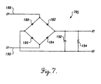
- FIGURE 7 is a circuit diagram of an exemplary high voltage rectifier 78j suitable for use in high voltage generator 50j.
- the high voltage rectifier comprises four high voltage diodes 180, 182, 184, and 186 that are connected in a full-bridge configuration.
- Input lines 188 and 190 of the bridge are connected to the secondary winding 76j of high voltage transformer 72j.
- the output lines from the bridge are connected across a parallel combination of a capacitor 192 and a resistor 194.
- a high voltage square pulse generated by inverter 70j and stepped-up by transformer 72j is applied across the input to the diode bridge.
- the full-wave rectified output from the bridge is then filtered and loaded by capacitor 192 and resistor 194.
- the rectified output from the Group III high voltage generator corresponds to the V 3 graph as shown in FIGURES 4 and 5.
- the eight Group II high voltage generators 50b, 50c, ...50i are constructed using a design nearly identical to the Group III high voltage generator 50j.
- Inverters 70b, 70c, ...70i are constructed substantially as shown in FIGURE 6.
- resistor 166 is selected so that the Group II inverters will not be disabled when the desired current is indicated in the load.
- the value of resistor 166 is instead selected to provide overcurrent protection for each high voltage generator.
- the Group II inverters 70b, 70c,... 70i produce an output voltage that is substantially identical to the square wave voltage produced by the timing generator.
- each high voltage generator 50b, 50c,... 50i are identical to the components in high voltage generator 50j.
- High voltage transformers 72b, 72c,... 72i are identical to transformer 72j, and rectifiers 78b, 78c,...78i correspond to the construction of rectifier 78j as shown in FIGURE 7.
- the square wave generated by the inverter is stepped-up by the transformer and full wave rectified by the rectifier.
- Each Group II high voltage generator therefore produces an approximately DC output voltage having an amplitude of 1,000 volts.
- Control circuit 56 is connected to each of the Group II high voltage generators 50b, 50c, ...50i.
- the control circuit is designed to monitor the voltage V c across the capacitive component of the load and to enable or disable the Group II high voltage generators so that the output voltage V 2 from the Group II generators is less than or equal to V c .
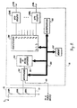
- FIGURE 8 is a block diagram of a control circuit suitable for monitoring the voltage drop across the capacitive component of the load and enabling or disabling additional Group II high voltage generators in the high voltage power supply.
- high voltage divider network 82 consists of resistors 200a, 200b, ... 200n connected in series between V c and ground.
- the resistors are selected such that the voltage drop across resistors 200b, 200c,... 200n reduces the voltage drop across resistor 200a to a desired level.
- the voltage across resistor 200a is provided on line 54 to control circuit 56.
- Control circuit 56 includes a multiplexer 202, an analog-to-digital converter 204, a demultiplexer 206, a microprocessor 205 and associated memory 207, and, in a preferred embodiment of the invention, eight optoisolators 208a, 208b, ... 208h.
- the control circuit components are coupled to each other by an address/data bus 203.
- Multiplexer 202 is connected to the high voltage divider network by line 54 and also to the AC power source 84 by line 101.
- the microprocessor may selectively sample the voltage V c across the capacitive components of the load or the output voltage V ac from the AC power source by switching multiplexer 202. The selected voltage is provided to analog-to-digital converter 204 on a line 201.
- the analog-to-digital converter generates a three-bit digital value that is representative of the magnitude of the selected voltage (V ac or V c ).
- resistors 200a, 200b, ... 200n should be selected so that the expected voltage variation across resistor 200a is within the input voltage range of analog-to-digital converter 204.
- the AC power source may similarly have to be scaled so that the scaled power source voltage falls within the range of the analog-to-digital converter.
- the digitized value corresponding to the selected voltage is provided to the microprocessor 205. Based on the value of the selected voltage, the microprocessor may enable or disable additional Group II high voltage generators. To enable or disable the high voltage generators, the microprocessor provides an appropriate command to demultiplexer 206 over bus 203.
- demultiplexer 206 is a 3 x 8 decoder that enables the output lines that correspond to the digital value received on the demultiplexer input lines.
- Each output line from the demultiplexer is coupled to an optoisolator 208a, 208b, ... 208h. The optoisolators are then coupled via lines 210a, 210b,...
- Optoisolators 208a, 208b, ... 208h are provided between demultiplexer 206 and high voltage generators 50b, 50c,... 50i to ensure that the high voltage produced in the high voltage generators is isolated from the logic circuitry in control circuit 56.
- a logic "1" on a demultiplexer output line turns on a corresponding high voltage generator, and a logic "0" on a demultiplexer output line turns off the corresponding high voltage generator.
- the determination of whether to enable or disable Group II high voltage generators is based on measured changes in the power supply voltage V ac or the voltage V c across the load.
- the control circuit must enable or disable the inverters in the Group II high voltage generators in order to ensure that the sum voltage generated by the Group II generators is equal to or less than the voltage V c . If V c increases, V ac decreases, or (V c - V ac ) increases, the control circuit will enable additional Group II high voltage generators by generating additional signals on lines210a, 210b,... 210h to bias ON triac 146 and the associated inverters 70b, 70c,... 70i.
- the control circuit will disable additional Group II high voltage generators by switching OFF one or more of the triacs in the high voltage generator inverters.
- the sum voltage produced by the Group II generators should not fall below the voltage V c by an amount greater than the maximum voltage that can be produced by the Group I generators (i.e., V c - V 2 ⁇ V 1 ). This ensures that the sum of the Group I and II generators will allow the output voltage V gen of the high voltage power supply to accurately track V c .
- the sum of the output voltages from the Group II high voltage generators corresponds to the V 2 graph shown in FIGURES 4 and 5.
- microprocessor 205 may filter or otherwise manipulate the measured values of the selected voltages.
- microprocessor 205 may also be coupled to sensors to detect when a Group II high voltage generator has failed. When a failure is detected, the microprocessor may dynamically enable an additional high voltage generator to replace the failed generator.
- the Group I high voltage generator 50a is constructed using a design nearly identical to the Group III high voltage generator 50j.
- Inverter 70a is constructed as shown in FIGURE 6. The only variation in inverter construction is that the value of resistor 166 is selected to provide overcurrent protection, rather than to set a desired current in the load.
- High voltage transformer 70a is constructed around a magnetic ferrite core, with a primary winding consisting of 90 turns and a secondary winding consisting of 640 turns. The additional turns in the secondary winding of high voltage transformer 70a increases the output voltage produced by the Group I high voltage generator to about 1,200 volts.
- Rectifier 78a corresponds to the construction of rectifier 78j as shown in FIGURE 7.
- the Group I high voltage generator is designed to produce an output voltage ranging between zero and a maximum value in order to track the difference in the voltage generated by the Group II high voltage generators and the voltage V c across the capacitive components in the load.
- the Group I high voltage generator produces a dynamically-varying high voltage.
- current control circuit 64 is provided to monitor and maintain a desired current through the high voltage generator.
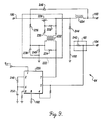
- a schematic diagram of a current control circuit suitable for monitoring and maintaining a desired current through the Group I high voltage generator is provided in FIGURE 9.
- the heart of the current control circuit is a PWM controller 220, which in a preferred embodiment of the invention is a Signetics NE5561.
- PWM controller 220 generates an internal sawtooth waveform voltage having a preferred frequency of 40 kHz for an inverter embodiment operating from a 20 kHz timing signal.
- the PWM controller frequency is determined by a resistor 248 and a capacitor 250 connected to the controller.
- the PWM controller 220 is connected to a switching network 222 that is used to connect and disconnect the DC voltage provided on line 100 with the inverter 70a through an inductor 224.
- Switching network 222 comprises a MOSFET transistor 226, having the drain electrode connected with line 100, and the base and source electrodes connected with inductor 224.
- the gate electrode of transistor 226 is connected to one lead of the secondary winding of a transformer 232 through a resistor 230.
- the other lead of the secondary winding is connected to the base and source electrodes of the transistor, and also to the gate electrode through a resistor 228.
- Resistor 230 limits the current applied to the gate of transistor 226, and resistor 228 creates a path for current flowing from the gate-to-source capacitance of the transistor to allow the transistor to switch to an OFF position more quickly.
- One lead of the primary winding of transformer 232 is connected across a resistor 240 and capacitor 238 to ground, and through a resistor 236 to line 100.
- a resistor 234 is connected in parallel with the primary winding. The other lead of the primary winding is connected to the PWM controller 220.
- transistor 226 is switched by PWM controller 220 to achieve discontinuous current flow through inductor 224 and inverter 70a.
- PWM controller When PWM controller is switched on, current is allowed to flow from line 100 through resistor 236 and the primary winding of transformer 232 and to ground via the PWM controller on line 102. This generates a positive voltage across the gate of transistor 226, biasing the transistor ON and allowing current to flow through inductor 224 and over line 103 to inverter 70a. After flowing through inverter 70a, the current flows through a line 104, a shunt resistor 242, and on line 102 to ground. As the magnitude of the current increases through the shunt resistor, the voltage drop across the resistor increases.
- a diode 246 is also provided in the current control circuit to protect the circuit from overvoltage.
- a diode 246 is also provided in the current control circuit to protect the circuit from overvoltage.
- Those skilled in the art will recognize that other circuits or techniques may be used to maintain a desired current level from the output of high voltage generator 50a.
- the output from the Group I high voltage generator corresponds to the V 1 graph as shown in FIGURES 4 and 5.
- the Group III high voltage generator may be constructed with a current fed inverter similar to the construction of the Group I high voltage generator.
- a current control circuit would control the output of the Group III high voltage generator to maintain a desired current through the generator.
- the current control circuit would increase the voltage generated by the Group III high voltage generator to raise the current level to a desired current I d .
- the output from the Group III generator would be switched off.
- a representative load is selected that has a resistive component of 20 kOhm, a capacitive component of 10 uF, and a inductive component of 6 x 10 -3 H.
- Each high voltage generator 50a, 50b,... 50j produces an output voltage of approximately 1,000 volts, thereby producing a potential maximum output voltage for the high voltage power supply of 10 kV.
- Timing generator 66 produces a square wave timing signal of approximately 15 kHz, having a period of 66 x 10 -6 seconds.
- the high voltage power supply enters the tracking mode.
- the Group II high voltage generators continue to generate an output voltage that is less than or equal to the voltage across the capacitive component of the load.
- the Group I high voltage generator generates the difference between the Group II output voltage and the voltage across the capacitive component of the load.
- the current in the load remains constant since there is no voltage drop across the inductive component of the load.
- a high voltage power supply formed in accordance with the present invention offers many advantages over the prior art. Because few energy storage elements are used to maintain the output voltage level at a desired value, the high voltage power supply of the present invention may be quickly switched on or off. The lack of energy storage elements also provides for a fast response time to variations in load voltage. The high voltage power supply of the present invention is therefore suitable for use in dynamic applications wherein the load has quickly varying capacitive, resistive, and inductive components.
- a further advantage is that the use of multiple high voltage generators to generate a desired output voltage allows the high voltage power supply to be tailored for each particular application.
- High voltage generators may be added to the Group II generators to increase maximum generated voltage and produce a greater dynamic range of the power supply.
- Control circuit 56 can similarly be expanded or reduced to control a greater or lesser number of high voltage generators.
- the ability to dynamically enable or disable high voltage generators also produces a number of operating advantages. Enabling or disabling high voltage generators allows the output voltage to be controlled to produce a desired waveform, making the power supply suitable for state-of-the-art radars and other similar applications.
- the high voltage generators may also be dynamically added or removed to smooth the effect from ripples in the low frequency input AC voltage. Using the high voltage generators to smooth the effect of input voltage ripples eliminates the need for large and expensive capacitive filters to regulate the input voltage.
- high voltage generators may also be substituted when other high voltage generators in the power supply fail. The dynamic replacement of substitute generators improves the overall reliability of the power supply.
- the preferred embodiment of the power supply contains only one high voltage generator in Groups I and III, those skilled in the art will recognize that in each group a number of high voltage generators could be connected in cascode fashion to create the desired output voltage.
- a control circuit could be provided to dynamically enable or disable the additional Group I and III high voltage generators, producing the attendant advantages described above with respect to the Group II generators.
- the preferred embodiment of the high voltage power supply has eight high voltage generators in Group II, the number of generators may be varied depending upon the expected load and load fluctuation.
- each high voltage transformer contained within each high voltage generator may be varied.
- the transformers may be constructed with a plurality of secondary windings.
- Each of the plurality of secondary windings may be coupled to a high voltage rectifier, and the output voltage of each high voltage rectifier summed to produce the output voltage of the high voltage generator.
- the primary winding of each transformer may also be constructed with a plurality of taps. Each of the taps may be coupled to the output from the high voltage generator inverter through a switch. By switching the desired tap from the primary winding into connection with the inverter, the output voltage from each high voltage generator may be selectively varied.
- V c across the capacitive component of the load was used as feedback in the preferred embodiment of the high voltage power supply
- other measures of the voltage or current in the load could be used as feedback to control the number of Group II generators that are enabled or disabled.
- a measure of the rate of charge or discharge of the capacitor in the load may be used as an indication of the current flowing in the load.
- a direct measurement may be made of the current magnitude or direction in the load.
- the actual parameter used to monitor the current in the load may depend on the availability and accessibility of the parameter in the load.
- each of the Group II generators may also be constructed to produce different output voltages.
- each of three Group II generators may be designed to produce 10,000 volts.
- the Group I generator must therefore also be designed to produce a maximum of 10,000 volts.
- the Group I generator in the preferred embodiment of the power supply includes a physically large inductor in which magnetic energy is stored, the size and weight of the power supply is increased.
- the three Group II generators may be designed to produce 17,100 volts, 8,600 volts, and 4,300 volts. The second construction would allow the Group I generator to only produce a maximum of 4,300 volts.
- the smaller output voltage decreases the size, weight, and stored energy of the Group I generator.
- the disclosed power supply design therefore offers tremendous flexibility in tailoring the power supply to a particular application.
Landscapes
- Engineering & Computer Science (AREA)
- General Health & Medical Sciences (AREA)
- Toxicology (AREA)
- Power Engineering (AREA)
- Health & Medical Sciences (AREA)
- Automation & Control Theory (AREA)
- Dc-Dc Converters (AREA)
- Generation Of Surge Voltage And Current (AREA)
- Inverter Devices (AREA)
- Details Of Television Scanning (AREA)
- Ignition Installations For Internal Combustion Engines (AREA)
- X-Ray Techniques (AREA)
- Electrostatic Separation (AREA)
Claims (35)
- Système d'alimentation à haute tension pour générer un courant réglé dans une charge qui a un composant capacitif, comprenant :(a) un circuit de synchronisation qui génère un signal de synchronisation répétitif, et(b) un générateur de tension pour générer une tension d'attaque et une tension de poursuite lors de chaque répétition du signal de synchronisation, le générateur de tension comprenant :(1) un premier générateur couplé à la charge et au circuit de synchronisation, le premier générateur générant et appliquant à la charge au moins une partie de la tension d'attaque, dans lequel on amène la tension d'attaque à dépasser une tension aux bornes du composant capacitif de la charge en synchronisme avec chaque répétition du signal de synchronisation et dans lequel la tension d'attaque induit un courant croissant dans la charge, la tension d'attaque étant appliquée jusqu'à ce que le courant dans la charge atteigne une grandeur souhaitée, après quoi la tension d'attaque n'est plus supérieure à la tension aux bornes du composant capacitif de la charge, et(ii) un second générateur couplé à la charge et au circuit de synchronisation et en cascode avec le premier générateur, le second générateur générant et appliquant à la charge au moins une partie de la tension de poursuite, dans lequel la tension de poursuite est amenée à varier avec les variations du courant passant par la charge après la génération de la tension d'attaque et dans lequel la tension de poursuite est sensiblement égale à une tension aux bornes du composant capacitif de la charge de sorte que le courant dans la charge soit maintenu à un niveau presque constant.
- Système d'alimentation à haute tension selon la revendication 1, dans lequel le premier générateur comprend :(a) au moins un générateur accélérateur pour générer une impulsion rectangulaire redressée comme tension de sortie, et(b) au moins un générateur de base couplé en cascode au générateur accélérateur pour générer une onde carrée redressée comme tension de sortie, dans lequel la somme de la tension de sortie du générateur accélérateur et de la tension de sortie du générateur de base dépasse une tension dans la charge et génère, par suite, un courant croissant dans la charge.
- Système d'alimentation à haute tension selon la revendication 1, dans lequel le second générateur comprend :(a) au moins un générateur de base pour générer une onde carrée redressée comme tension de sortie, l'onde carrée redressée ayant une amplitude inférieure ou égale à celle d'une tension aux bornes du composant capacitif de la charge, et(b) au moins un générateur de poursuite couplé en cascode au générateur de base pour générer une tension équivalent à la différence entre la tension de sortie produite par le générateur de base et la tension aux bornes du composant capacitif de la charge, dans lequel la somme de la tension de sortie produite par le générateur de base et de la tension de sortie produite par le générateur de poursuite est sensiblement égale à la tension aux bornes du composant capacitif de la charge.
- Système d'alimentation à haute tension selon la revendication 1, dans lequel le signal de synchronisation répétitif est un signal périodique.
- Système d'alimentation à haute tension selon la revendication 1, dans lequel :(a) le circuit de synchronisation comprend un générateur de synchronisation qui produit un signal de synchronisation répétitif, dans lequel, lors de chaque répétition du signal de synchronisation, le système d'alimentation à haute tension effectue un cycle passant par un mode d'attaque où la tension de sortie du système d'alimentation dépasse une tension aux bornes du composant capacitif de la charge et un mode de poursuite où la tension de sortie du système d'alimentation est sensiblement égale à la tension aux bornes du composant capacitif de la charge, et(b) le générateur de tension comprend en outre une pluralité de générateurs de haute tension, la pluralité de générateurs de haute tension formant le premier et le second générateurs, la pluralité de générateurs de haute tension étant couplée en cascode à la charge de telle sorte que les tensions de sortie produites par la pluralité de générateurs de haute tension soient sommées les unes avec les autres, dans lequel, lors du mode de fonctionnement en entraínement, les générateurs de haute tension produisent une tension de sortie qui dépasse la tension aux bornes du composant capacitif de la charge, provoquant ainsi un courant croissant dans la charge jusqu'à ce que le courant atteigne un niveau souhaité, après quoi les générateurs de haute tension entrent dans le mode de fonctionnement en poursuite dans lequel les générateurs de haute tension produisent une tension de sortie sensiblement égale à la tension aux bornes du composant capacitif de la charge, provoquant de la sorte le maintien d'un courant dans la charge au niveau souhaité, chacun de la pluralité de générateurs de haute tension comprenant :(i) un inverseur ayant une entrée connectée à ladite source d'alimentation CC et une entrée couplée audit générateur de synchronisation et produisant une tension CA en synchronisme avec le signal de synchronisation;(ii) un transformateur couplé à l'inverseur pour transformer la tension CA produite par l'inverseur, et(iv) un redresseur couplé à l'inverseur pour redresser la tension CA produite par l'inverseur.
- Système d'alimentation à haute tension selon la revendication 1, dans lequel le circuit de synchronisation comprend un générateur de synchronisation qui produit un signal de synchronisation répétitif, dans lequel, lors de chaque répétition du signal de synchronisation, le système d'alimentation effectue un cycle passant par un mode d'attaque où la tension de sortie du système d'alimentation dépasse une tension aux bornes de la partie de composant capacitif de la charge et un mode de poursuite où la tension de sortie du système d'alimentation est sensiblement égale à la tension aux bornes de la pute de composant capacitif de la charge.
- Système d'alimentation à haute tension selon la revendication 6, dans lequel le premier générateur comprend :(a) au moins un générateur de base connecté au générateur de synchronisation, le générateur de base produisant une tension de base qui est réglée à un niveau de tension proche de la tension aux bornes de la partie de composant capacitif de la charge lors du mode d'attaque et du mode de poursuite, et(b) au moins un générateur accélérateur connecté au générateur de synchronisation et couplé en cascode au générateur de base, le générateur accélérateur produisant une tension accélératrice qui augmente la tension de sortie totale du système d'alimentation à une tension supérieure à celle aux bornes de la partie de composant capacitif de la charge au cours du mode d'attaque.
- Système d'alimentation à haute tension selon la revendication 6, dans lequel le second générateur comprend :(a) au moins un générateur de poursuite connecté au générateur de synchronisation et produisant une tension de poursuite qui varie avec les variations de la tension aux bornes de la partie de composant capacitif de la charge au cours du mode de poursuite, et(b) au moins un générateur de base connecté au générateur de synchronisation et couplé en cascode au générateur de poursuite, le générateur de base produisant une tension de base qui est réglée à un niveau de tension proche de la tension aux bornes de la partie de composant capacitif de la charge lors du mode d'attaque et du mode de poursuite.
- Système d'alimentation à haute tension selon la revendication 6, dans lequel :(a) le premier générateur comprend au moins un générateur accélérateur connecté au générateur de synchronisation, le générateur accélérateur produisant une tension accélératrice qui augmente la tension de sortie totale du système d'alimentation à une tension supérieure à celle aux bornes de la partie de composant capacitif de la charge au cours du mode d'attaque, et(b) le second générateur comprend au moins un générateur de poursuite connecté au générateur de synchronisation et produisant une tension de poursuite qui varie avec les variations de la tension aux bornes de la partie de composant capacitif de la charge au cours du mode de poursuite.
- Système d'alimentation à haute tension selon la revendication 9, dans lequel le premier générateur comprend en outre au moins un générateur de base connecté au générateur de synchronisation et couplé en cascode au générateur de poursuite, le générateur de base produisant une tension de base qui est réglée à un niveau de tension proche de la tension aux bornes de la partie de composant capacitif de la charge lors du mode d'attaque et du mode de poursuite.
- Système d'alimentation à haute tension selon la revendication 9, dans lequel le second générateur comprend en outre au moins un générateur de base connecté au générateur de synchronisation et couplé en cascode au générateur de poursuite, le générateur de base produisant une tension de base qui est réglée à un niveau de tension proche de la tension aux bornes de la partie de composant capacitif de la charge lors du mode d'attaque et du mode de poursuite.
- Système d'alimentation à haute tension selon la revendication 9, comprenant en outre un ou plusieurs générateurs de base connectés au générateur de synchronisation, au moins un générateur de base étant couplé en cascode au générateur accélérateur et produisant une tension de base qui est réglée à un niveau de tension proche de la tension aux bornes de la partie de composant capacitif de la charge lors du mode d'attaque, et au moins un générateur de base étant couplé en cascode au générateur de poursuite et produisant une tension de base qui est réglée à un niveau de tension proche de la tension aux bornes de la partie de composant capacitif de la charge lors du mode de poursuite.
- Système d'alimentation à haute tension selon la revendication 6, dans laquelle le générateur de tension comprend en outre :les générateurs de poursuite, de base et d'accélération formant le premier et le second générateurs.(a) au moins un générateur de poursuite connecté au générateur de synchronisation et produisant une tension de poursuite qui varie avec les variations de la tension aux bornes de la partie de composant capacitif de la charge lors du mode de poursuite, et(b) au moins un générateur de base connecté au générateur de synchronisation et couplé en cascode au générateur de poursuite, le générateur de base produisant une tension de base qui est réglée à un niveau de tension proche de la tension aux bornes de la partie de composant capacitif de la charge lors du mode d'attaque et du mode de poursuite, et(c) au moins un générateur accélérateur connecté au générateur de synchronisation et couplé en cascode aux générateurs de poursuite et de base, le générateur de base produisant une tension accélératrice qui augmente la tension de sortie totale du système d'alimentation à une tension supérieure à celle aux bornes de la partie de composant capacitif de la charge lors du mode de poursuite.
- Système d'alimentation à haute tension selon les revendications 10, 11, 12 ou 13, dans lequel une tension de sortie produite par le système d'alimentation est égale à la somme de la tension de poursuite, de la tension de base et de la tension accélératrice produites par le générateur de poursuite, le générateur de base et le générateur accélérateur de telle sorte qu'au cours du mode d'attaque, la tension de sortie du système d'alimentation dépasse la tension aux bornes de la partie de composant capacitif de la charge de manière à élever le courant dans la charge à un niveau souhaité et qu'au cours du mode de poursuite, la tension de sortie du système d'alimentation soit sensiblement égale à la tension aux bornes du composant capacitif de la charge de manière à maintenir le courant dans la charge sensiblement au niveau souhaité.
- Système d'alimentation selon la revendication 14, dans lequel le générateur de base comprend une pluralité de générateurs de haute tension couplés en cascode les uns avec les autres.
- Système d'alimentation selon la revendication 15, dans lequel chacun de la pluralité de générateurs de haute tension génère une tension de sortie qui est sensiblement égale.
- Système d'alimentation selon la revendication 15, dans lequel certains de la pluralité de générateurs de haute tension génèrent une tension de sortie qui a une grandeur différente.
- Système d'alimentation selon la revendication 15, comprenant en outre un circuit de commande couplé à la pluralité de générateurs de haute tension et à la charge, ledit circuit de commande commandant un paramètre d'énergie électrique aux bornes d'une partie constituante de la charge et activant ou désactivant un générateur choisi dans la pluralité de générateurs de haute tension en réponse aux variations du paramètre d'énergie électrique aux bornes de la partie constituante de la charge.
- Système d'alimentation selon la revendication 18, dans lequel le circuit de commande contrôle en outre un état opératoire de chaque générateur de haute tension et active un générateur de haute tension supplémentaire si l'état opératoire indique qu'un générateur de haute tension est tombé en panne.
- Système d'alimentation selon la revendication 18, dans lequel le circuit de commande contrôle en outre une tension d'entrée dans. le système d'alimentation et active ou désactive un nombre souhaité de la pluralité de générateurs de haute tension en réponse aux variations de la tension d'entrée.
- Système d'alimentation selon la revendication 18, dans lequel le circuit de commande maintient la tension de base produite par la pluralité de générateurs de haute tension à un niveau inférieur ou égal à la tension aux bornes de la partie constituante de la charge contrôlée par le circuit de commande.
- Système d'alimentation selon la revendication 15, comprenant en outre une source de courant CC connectée pour délivrer un courant de fonctionnement au système d'alimentation.
- Système d'alimentation selon la revendication 22, dans lequel chacun de la pluralité de générateurs de haute tension comprend :(a) un inverseur ayant une première entrée couplée à une source de courant CC et une seconde entrée couplée au générateur de synchronisation,(b) un transformateur ayant un enroulement primaire couplé à une sortie de l'inverseur, et(c) un redresseur couplé à un enroulement secondaire du transformateur.
- Système d'alimentation selon la revendication 23, dans lequel chacun de la pluralité de générateurs de haute tension génère une tension de sortie à onde carrée redressée en synchronisme avec le signal de synchronisation généré par le générateur de synchronisation.
- Système d'alimentation selon la revendication 23, dans lequel l'enroulement primaire du transformateur comprend une pluralité de prises qui sont couplées à la sortie de l'inverseur par une pluralité de commutateurs.
- Système d'alimentation selon la revendication 22, comprenant en outre un circuit de commande de courant couplé entre la source de courant CC et le générateur accélérateur.
- Système d'alimentation selon la revendication 22, comprenant en outre un circuit de commande de courant couplé entre la source de courant CC et le générateur de poursuite.
- Système d'alimentation selon la revendication 27, dans lequel le générateur de poursuite comprend :(a) un inverseur ayant une première entrée couplée au régulateur de courant constant et une seconde entrée couplée au générateur de synchronisation, le régulateur de courant constant maintenant un courant dans l'inverseur à un niveau souhaité,(b) un transformateur ayant un enroulement primaire couplé à une sortie de l'inverseur, et(c) un redresseur couplé à un enroulement secondaire du transformateur.
- Système d'alimentation selon la revendication 28, dans lequel le générateur de poursuite produit une tension de poursuite sensiblement égale à une tension aux bornes du composant capacitif de la charge moins la tension de base produite par le générateur de base.
- Système d'alimentation selon la revendication 22, dans lequel le générateur accélérateur comprend :(a) un inverseur ayant une première entrée couplée à une source de courant CC et une seconde entrée couplée au générateur de synchronisation,(b) un transformateur ayant un enroulement primaire couplé à une sortie de l'inverseur,(c) un redresseur couplé à un enroulement secondaire du transformateur,(d) un circuit de réaction couplé à l'inverseur, le circuit de réaction contrôlant un courant du système d'alimentation et désactivant le générateur accélérateur si un niveau de courant souhaité est atteint.
- Système d'alimentation selon la revendication 30, dans lequel le générateur accélérateur produit une impulsion carrée périodique.
- Système d'alimentation selon la revendication 14, dans lequel le signal de synchronisation répétitif est un signal périodique.
- Système d'alimentation selon la revendication 14, dans lequel la charge comprend une pluralité de composants capacitifs, le composant capacitif aux bornes duquel la tension est dépassée par la sortie du système d'alimentation au cours du mode d'attaque et aux bornes duquel la tension est sensiblement égale à la sortie du système d'alimentation au cours du mode de poursuite comprenant deux composants capacitifs ou plus en série.
- Système d'alimentation selon la revendication 14, dans lequel le générateur de poursuite comprend une pluralité de générateurs de haute tension couplés en cascode pour produire la tension de poursuite.
- Système d'alimentation selon la revendication 14, dans lequel le générateur accélérateur comprend une pluralité de générateurs de haute tension couplés en cascode pour produire la tension accélératrice.
Applications Claiming Priority (3)
| Application Number | Priority Date | Filing Date | Title |
|---|---|---|---|
| US08/416,997 US5629844A (en) | 1995-04-05 | 1995-04-05 | High voltage power supply having multiple high voltage generators |
| US416997 | 1995-04-05 | ||
| PCT/US1996/004691 WO1996031939A1 (fr) | 1995-04-05 | 1996-04-05 | Source d'alimentation a haute tension possedant plusieurs generateurs de haute tension |
Publications (2)
| Publication Number | Publication Date |
|---|---|
| EP0819336A1 EP0819336A1 (fr) | 1998-01-21 |
| EP0819336B1 true EP0819336B1 (fr) | 2000-09-13 |
Family
ID=23652173
Family Applications (1)
| Application Number | Title | Priority Date | Filing Date |
|---|---|---|---|
| EP96912581A Expired - Lifetime EP0819336B1 (fr) | 1995-04-05 | 1996-04-05 | Source d'alimentation a haute tension possedant plusieurs generateurs de haute tension |
Country Status (9)
| Country | Link |
|---|---|
| US (2) | US5629844A (fr) |
| EP (1) | EP0819336B1 (fr) |
| JP (1) | JPH11503299A (fr) |
| CN (1) | CN1056483C (fr) |
| AT (1) | ATE196394T1 (fr) |
| AU (1) | AU697683B2 (fr) |
| CA (1) | CA2216168C (fr) |
| DE (1) | DE69610298T2 (fr) |
| WO (1) | WO1996031939A1 (fr) |
Families Citing this family (64)
| Publication number | Priority date | Publication date | Assignee | Title |
|---|---|---|---|---|
| US5629844A (en) * | 1995-04-05 | 1997-05-13 | International Power Group, Inc. | High voltage power supply having multiple high voltage generators |
| JPH0926121A (ja) * | 1995-07-14 | 1997-01-28 | Tokyo Yogyo Co Ltd | ゴミ焼却炉 |
| US5751150A (en) * | 1995-08-11 | 1998-05-12 | Aerovironment | Bidirectional load and source cycler |
| DE69523752T2 (de) * | 1995-08-31 | 2002-08-29 | St Microelectronics Srl | Verfahren und Schaltung zur pulsbreitenmodulierten Steuerung einer Brücke und eines Plattenantriebs und unter Verwendung derselben |
| US5905645A (en) * | 1996-12-02 | 1999-05-18 | Astec International Limited | Thermally aided power sharing of power supplies with or without an external current share line |
| DE19720948A1 (de) * | 1997-05-17 | 1998-11-19 | Bosch Gmbh Robert | Vorrichtung zur Spannungswandlung |
| US5917719A (en) * | 1997-08-11 | 1999-06-29 | Power Ten, Inc. | Internally programmable modular power supply and method |
| KR100343983B1 (ko) * | 1999-06-29 | 2002-07-22 | 엘지산전 주식회사 | 고전압, 대전류 펄스 발생장치의 출력제어 및 보호회로 |
| DE19961541A1 (de) * | 1999-12-20 | 2001-07-19 | Magnet Motor Gmbh | Hochspannungswandler |
| US7615893B2 (en) * | 2000-05-11 | 2009-11-10 | Cameron International Corporation | Electric control and supply system |
| DE20115474U1 (de) | 2001-09-19 | 2003-02-20 | Biester, Klaus, 29342 Wienhausen | Gleichspannungs-Wandlervorrichtung |
| DE20115471U1 (de) * | 2001-09-19 | 2003-02-20 | Biester, Klaus, 29342 Wienhausen | Universelles Energieversorgungssystem |
| DE20018560U1 (de) * | 2000-10-30 | 2002-03-21 | CAMERON GmbH, 29227 Celle | Steuer- und Versorgungssystem |
| DE20115473U1 (de) * | 2001-09-19 | 2003-02-20 | Biester, Klaus, 29342 Wienhausen | Universelles Energieversorgungssystem |
| US6297977B1 (en) * | 2000-09-12 | 2001-10-02 | Honeywell Power Systems Inc. | Parallel operation of multiple generators |
| US6531852B2 (en) * | 2000-09-22 | 2003-03-11 | Interuniversitair Microelektronica Centrum (Imec) | Device and method for generating a high voltage |
| JP2002101560A (ja) * | 2000-09-26 | 2002-04-05 | Honda Motor Co Ltd | 発電装置 |
| GB2417373B (en) * | 2001-09-19 | 2006-04-26 | Cooper Cameron Corp | Dc converter |
| US7020271B2 (en) * | 2003-06-12 | 2006-03-28 | Barbara Isabel Hummel | Ring control device |
| DE20115475U1 (de) * | 2001-09-19 | 2003-02-20 | Biester, Klaus, 29342 Wienhausen | Gleichspannungs-Wandlervorrichtung |
| US6738268B1 (en) * | 2001-11-28 | 2004-05-18 | Emc Corporation | Method and apparatus for providing power signals to operating circuitry mounted on circuit boards |
| GB0208485D0 (en) * | 2002-04-12 | 2002-05-22 | Cit Alcatel | Power feed |
| US20040125618A1 (en) * | 2002-12-26 | 2004-07-01 | Michael De Rooij | Multiple energy-source power converter system |
| JP3845405B2 (ja) * | 2003-09-26 | 2006-11-15 | Necマイクロ波管株式会社 | 進行波管用電源装置 |
| JP4461824B2 (ja) * | 2004-02-13 | 2010-05-12 | トヨタ自動車株式会社 | 自動車、自動車の制御方法、制御方法をコンピュータに実行させるためのプログラムを記録したコンピュータ読取可能な記録媒体 |
| US7480487B2 (en) * | 2005-05-20 | 2009-01-20 | Dresser, Inc. | Power regulation for field instruments |
| US20060265105A1 (en) * | 2005-05-20 | 2006-11-23 | Hughes Albert R | Loop-powered field instrument |
| FR2887922A1 (fr) * | 2005-07-01 | 2007-01-05 | Renault Sas | Ensemble d'agglomeration et de collection des particules contenues dans des gaz d'echappement d'un moteur a combustion interne de vehicule automobile pourvu d'un dispositif d'alimentation electrique haute tension |
| JP5604103B2 (ja) * | 2006-08-31 | 2014-10-08 | コーニンクレッカ フィリップス エヌ ヴェ | X線生成システムの電源 |
| US7785404B2 (en) * | 2006-10-02 | 2010-08-31 | Sylmark Holdings Limited | Ionic air purifier with high air flow |
| US8305781B2 (en) * | 2008-04-30 | 2012-11-06 | Hamilton Sundstrand Corporation | Inverter with high frequency isolation transformer |
| US20090322301A1 (en) * | 2008-06-26 | 2009-12-31 | Enermax Technology Corporation | Control circuit for improving efficiency of lower load of power supply device and method thereof |
| WO2010005291A1 (fr) * | 2008-07-11 | 2010-01-14 | Eldolab Holding B.V. | Convertisseur d'énergie pour un ensemble led et application d'éclairage |
| DE102008050350A1 (de) * | 2008-10-02 | 2010-04-08 | Yxlon International X-Ray Gmbh | Hochspannungssystem zum Einstellen eines Hochspannungspotenzials |
| GB2474447B (en) * | 2009-10-13 | 2014-12-10 | Mtu Friedrichshafen Gmbh | Generating set preloader |
| CN101961681B (zh) * | 2010-05-28 | 2012-10-24 | 宁波市镇海华泰电器厂 | 自动换极的高压电源 |
| CN102062829A (zh) * | 2010-09-25 | 2011-05-18 | 珠海市科荟电器有限公司 | 一种电网仿真检测装置 |
| EP2530805B1 (fr) | 2011-05-30 | 2017-06-21 | Schleifring und Apparatebau GmbH | Joint rotatif sans contact avec fonction de sécurité |
| WO2012169046A1 (fr) * | 2011-06-09 | 2012-12-13 | 東芝三菱電機産業システム株式会社 | Système d'alimentation sans coupure |
| CN103037606A (zh) * | 2011-10-10 | 2013-04-10 | 上海良治电器技术有限公司 | 一种新型高压发生器系统 |
| WO2013065703A1 (fr) * | 2011-11-04 | 2013-05-10 | 株式会社 日立メディコ | Appareil haute tension à rayons x et son procédé de fonctionnement |
| CN102590777A (zh) * | 2012-02-23 | 2012-07-18 | 江苏三通仪器系统有限公司 | 一种高压信号发生器 |
| CN103312187B (zh) * | 2012-03-09 | 2016-02-03 | 台达电子工业股份有限公司 | 一种变流器系统 |
| CN103906333B (zh) * | 2012-12-28 | 2016-08-03 | 台达电子工业股份有限公司 | X光管电源装置、具有该装置的电源系统及其操作方法 |
| US9983602B2 (en) * | 2012-12-31 | 2018-05-29 | Nvidia Corporation | Efficient voltage sensing systems and methods |
| CN104104243A (zh) * | 2013-04-02 | 2014-10-15 | 通用电气公司 | 模块式高压发电系统 |
| US9831198B2 (en) | 2013-08-22 | 2017-11-28 | Nvidia Corporation | Inductors for integrated voltage regulators |
| US10978955B2 (en) * | 2014-02-28 | 2021-04-13 | Eagle Harbor Technologies, Inc. | Nanosecond pulser bias compensation |
| CN103611632B (zh) * | 2013-12-11 | 2016-01-20 | 江苏科技大学 | 高频高压静电除尘电源 |
| JP6479438B2 (ja) * | 2014-11-25 | 2019-03-06 | キヤノンメディカルシステムズ株式会社 | X線高電圧装置、x線コンピュータ断層撮影装置、及びx線診断装置 |
| US10262829B2 (en) * | 2015-12-14 | 2019-04-16 | General Electric Company | Protection circuit assembly and method for high voltage systems |
| DE102017212224B4 (de) * | 2016-08-23 | 2019-10-31 | Siemens Healthcare Gmbh | Hochspannungsgenerator für ein Röntgengerät |
| US10224716B2 (en) * | 2016-10-04 | 2019-03-05 | Indian Institute Of Technology Bombay | Apparatus for generating AC superimposed DC signal |
| CN106423567B (zh) * | 2016-12-05 | 2018-10-19 | 福建龙净环保股份有限公司 | 一种高压电源组控制方法及控制系统 |
| CH713394A1 (de) * | 2017-01-30 | 2018-07-31 | Clean Air Entpr Ag | Elektrofilter. |
| JP6902167B2 (ja) | 2017-08-25 | 2021-07-14 | イーグル ハーバー テクノロジーズ, インク.Eagle Harbor Technologies, Inc. | ナノ秒パルスを使用する任意波形の発生 |
| CN108421642A (zh) * | 2018-04-27 | 2018-08-21 | 浙江大维高新技术股份有限公司 | 一种电除尘用高压脉冲电源 |
| US11810761B2 (en) | 2018-07-27 | 2023-11-07 | Eagle Harbor Technologies, Inc. | Nanosecond pulser ADC system |
| US11872727B2 (en) | 2020-04-07 | 2024-01-16 | Yi Hsuan Sung | Artificial botanicals and methods of making same |
| US11967484B2 (en) | 2020-07-09 | 2024-04-23 | Eagle Harbor Technologies, Inc. | Ion current droop compensation |
| DE102022103550B4 (de) | 2022-02-15 | 2024-01-04 | Woco Gmbh & Co. Kg | Ansteuerschaltung für einen Elektroabscheider |
| US11824542B1 (en) | 2022-06-29 | 2023-11-21 | Eagle Harbor Technologies, Inc. | Bipolar high voltage pulser |
| JP7833099B2 (ja) | 2022-09-29 | 2026-03-18 | イーグル ハーバー テクノロジーズ,インク. | 高電圧プラズマ制御 |
| EP4391728A1 (fr) * | 2022-12-19 | 2024-06-26 | Koninklijke Philips N.V. | Commande de courant d'émission pour générateurs haute tension |
Family Cites Families (21)
| Publication number | Priority date | Publication date | Assignee | Title |
|---|---|---|---|---|
| US3818307A (en) * | 1972-07-31 | 1974-06-18 | Bell Telephone Labor Inc | Serially-connected converters having multiple regulation modes for use in supplying serially-connected loads on long lines |
| DE3027172A1 (de) * | 1980-07-17 | 1982-02-18 | Siemens AG, 1000 Berlin und 8000 München | Verfahren zum betrieb eines elektrofilters |
| FR2499333A1 (fr) * | 1981-02-04 | 1982-08-06 | Cii Honeywell Bull | Dispositif automatique de compensation des variations de tension du secteur alternatif polyphase applique a un convertisseur alternatif continu |
| US4399392A (en) * | 1982-02-26 | 1983-08-16 | Gte Laboratories Incorporated | Arc lamp power supply |
| US4601051A (en) * | 1983-12-22 | 1986-07-15 | General Electric Company | Protective circuit for X-ray generator |
| JPS60156270A (ja) * | 1984-01-25 | 1985-08-16 | Hitachi Ltd | 電力変換装置の駆動制御装置 |
| HU197130B (en) * | 1985-04-11 | 1989-02-28 | Adam Kovacs | Circuit arrangement for generating pulses |
| ZA862614B (en) * | 1986-04-08 | 1986-12-30 | David John Cockram | Controller for gas discharge lamps |
| US4662343A (en) * | 1986-04-28 | 1987-05-05 | Smith Kenneth H | Method and apparatus for generating high voltage pulses |
| US4761725A (en) * | 1986-08-01 | 1988-08-02 | Unisys Corporation | Digitally controlled A.C. to D.C. power conditioner |
| US4999547A (en) * | 1986-09-25 | 1991-03-12 | Innovative Controls, Incorporated | Ballast for high pressure sodium lamps having constant line and lamp wattage |
| EP0261663B1 (fr) * | 1986-09-26 | 1992-06-17 | Hitachi, Ltd. | Dispositif à laser avec générateur d'impulsion haute-tension, générateur d'impulsion haute-tension et méthode de génération d'impulsion |
| US4933825A (en) * | 1987-04-09 | 1990-06-12 | Isco, Inc. | Power supply |
| EP0383962A1 (fr) * | 1989-02-20 | 1990-08-29 | Hauzer Holding B.V. | Redresseur à haute tension et électronique de commande correspondante |
| US5272612A (en) * | 1989-06-30 | 1993-12-21 | Kabushiki Kaisha Toshiba | X-ray power supply utilizing A.C. frequency conversion to generate a high D.C. voltage |
| US5128593A (en) * | 1990-01-25 | 1992-07-07 | Beckman Instruments, Inc. | Power supply for gas-filled lamps |
| WO1992003898A1 (fr) * | 1990-08-17 | 1992-03-05 | Gaslamp Power And Light | Systeme servant a fournir un courant de niveau constant a un tube fluorescent |
| FR2667723B1 (fr) * | 1990-10-09 | 1992-11-27 | Gen Electric Cgr | Dispositif d'obtention et de commutation de hautes tensions de polarisation d'electrodes de tube a rayons x. |
| JP2812824B2 (ja) * | 1990-11-14 | 1998-10-22 | 三菱電機株式会社 | 直流−直流変換器 |
| DE59206742D1 (de) * | 1992-01-20 | 1996-08-14 | Siemens Ag | Energieversorgungsverfahren für einen Elektrofilter |
| US5629844A (en) * | 1995-04-05 | 1997-05-13 | International Power Group, Inc. | High voltage power supply having multiple high voltage generators |
-
1995
- 1995-04-05 US US08/416,997 patent/US5629844A/en not_active Expired - Fee Related
-
1996
- 1996-04-05 DE DE69610298T patent/DE69610298T2/de not_active Expired - Fee Related
- 1996-04-05 AU AU55354/96A patent/AU697683B2/en not_active Ceased
- 1996-04-05 CA CA002216168A patent/CA2216168C/fr not_active Expired - Fee Related
- 1996-04-05 US US08/628,876 patent/US5737197A/en not_active Expired - Fee Related
- 1996-04-05 AT AT96912581T patent/ATE196394T1/de active
- 1996-04-05 CN CN96193066A patent/CN1056483C/zh not_active Expired - Fee Related
- 1996-04-05 WO PCT/US1996/004691 patent/WO1996031939A1/fr not_active Ceased
- 1996-04-05 JP JP8530495A patent/JPH11503299A/ja active Pending
- 1996-04-05 EP EP96912581A patent/EP0819336B1/fr not_active Expired - Lifetime
Also Published As
| Publication number | Publication date |
|---|---|
| US5629844A (en) | 1997-05-13 |
| CA2216168A1 (fr) | 1996-10-10 |
| WO1996031939A1 (fr) | 1996-10-10 |
| ATE196394T1 (de) | 2000-09-15 |
| EP0819336A1 (fr) | 1998-01-21 |
| AU697683B2 (en) | 1998-10-15 |
| CN1056483C (zh) | 2000-09-13 |
| DE69610298D1 (de) | 2000-10-19 |
| AU5535496A (en) | 1996-10-23 |
| CN1183862A (zh) | 1998-06-03 |
| US5737197A (en) | 1998-04-07 |
| DE69610298T2 (de) | 2001-04-12 |
| CA2216168C (fr) | 2000-06-27 |
| JPH11503299A (ja) | 1999-03-23 |
Similar Documents
| Publication | Publication Date | Title |
|---|---|---|
| EP0819336B1 (fr) | Source d'alimentation a haute tension possedant plusieurs generateurs de haute tension | |
| US4939381A (en) | Power supply system for negative impedance discharge load | |
| US5255179A (en) | Switched mode power supply for single-phase boost commercial AC users in the range of 1 kw to 10 kw | |
| US5724237A (en) | Apparatus and method for sharing a load current among frequency-controlled D.C.-to-D.C. converters | |
| US6163019A (en) | Resonant frequency induction furnace system using capacitive voltage division | |
| US5483142A (en) | Precharge circuit having microprocessor-based firing angle control circuitry | |
| EP0595091B1 (fr) | Redresseur triphasé actif | |
| EP0498631A2 (fr) | Alimentation électrique résonnante, à haute tension et deux modes d'opération | |
| US5639294A (en) | Method for controlling the power supply to an electrostatic precipitator | |
| JPH0865889A (ja) | 電力変換装置及び方法 | |
| KR950035037A (ko) | 유도부하에 대한 제어회로 | |
| JPH0523040B2 (fr) | ||
| DE60023183T2 (de) | Tragbarer generator | |
| EP0125278B1 (fr) | Alimentation ayant une source de courant continu d'entree et des etages d'alimentation a courant pulse | |
| GB2294165A (en) | Power supply for providing a dc supply from a multiphase ac source | |
| EP0813767A1 (fr) | Alimentation en mode commute a preconvertisseur synchrone | |
| RU2155425C1 (ru) | Зарядное устройство конденсаторной батареи | |
| EP1690327B1 (fr) | Convertisseur continu-continu sans regulation, a redressement synchrone avec commande de grille efficace | |
| US10530236B2 (en) | Auxiliary power supply for a gate driver | |
| US4258308A (en) | Switching regulator with flyback control offset | |
| JP3594723B2 (ja) | 電源装置 | |
| JPH0564040B2 (fr) | ||
| US4639662A (en) | Thyristor circuit for current regulation | |
| JP2663535B2 (ja) | アーク加工用電源装置 | |
| SU1742968A1 (ru) | Источник питани дл технологических установок посто нного тока |
Legal Events
| Date | Code | Title | Description |
|---|---|---|---|
| PUAI | Public reference made under article 153(3) epc to a published international application that has entered the european phase |
Free format text: ORIGINAL CODE: 0009012 |
|
| 17P | Request for examination filed |
Effective date: 19971024 |
|
| AK | Designated contracting states |
Kind code of ref document: A1 Designated state(s): AT BE CH DE DK ES FI FR GB GR IE IT LI LU MC NL PT SE |
|
| AX | Request for extension of the european patent |
Free format text: AL PAYMENT 971024;LT PAYMENT 971024;LV PAYMENT 971024;SI PAYMENT 971024 |
|
| RIN1 | Information on inventor provided before grant (corrected) |
Inventor name: SINITSYNA, IRINA, Z. Inventor name: KRICHTAFOVITCH, IGOR, A. |
|
| 17Q | First examination report despatched |
Effective date: 19980715 |
|
| GRAG | Despatch of communication of intention to grant |
Free format text: ORIGINAL CODE: EPIDOS AGRA |
|
| GRAG | Despatch of communication of intention to grant |
Free format text: ORIGINAL CODE: EPIDOS AGRA |
|
| GRAH | Despatch of communication of intention to grant a patent |
Free format text: ORIGINAL CODE: EPIDOS IGRA |
|
| GRAH | Despatch of communication of intention to grant a patent |
Free format text: ORIGINAL CODE: EPIDOS IGRA |
|
| GRAA | (expected) grant |
Free format text: ORIGINAL CODE: 0009210 |
|
| AK | Designated contracting states |
Kind code of ref document: B1 Designated state(s): AT BE CH DE DK ES FI FR GB GR IE IT LI LU MC NL PT SE |
|
| AX | Request for extension of the european patent |
Free format text: AL PAYMENT 19971024;LT PAYMENT 19971024;LV PAYMENT 19971024;SI PAYMENT 19971024 |
|
| PG25 | Lapsed in a contracting state [announced via postgrant information from national office to epo] |
Ref country code: NL Free format text: LAPSE BECAUSE OF FAILURE TO SUBMIT A TRANSLATION OF THE DESCRIPTION OR TO PAY THE FEE WITHIN THE PRESCRIBED TIME-LIMIT Effective date: 20000913 Ref country code: LI Free format text: LAPSE BECAUSE OF FAILURE TO SUBMIT A TRANSLATION OF THE DESCRIPTION OR TO PAY THE FEE WITHIN THE PRESCRIBED TIME-LIMIT Effective date: 20000913 Ref country code: IT Free format text: LAPSE BECAUSE OF FAILURE TO SUBMIT A TRANSLATION OF THE DESCRIPTION OR TO PAY THE FEE WITHIN THE PRESCRIBED TIME-LIMIT;WARNING: LAPSES OF ITALIAN PATENTS WITH EFFECTIVE DATE BEFORE 2007 MAY HAVE OCCURRED AT ANY TIME BEFORE 2007. THE CORRECT EFFECTIVE DATE MAY BE DIFFERENT FROM THE ONE RECORDED. Effective date: 20000913 Ref country code: FR Free format text: LAPSE BECAUSE OF FAILURE TO SUBMIT A TRANSLATION OF THE DESCRIPTION OR TO PAY THE FEE WITHIN THE PRESCRIBED TIME-LIMIT Effective date: 20000913 Ref country code: FI Free format text: LAPSE BECAUSE OF FAILURE TO SUBMIT A TRANSLATION OF THE DESCRIPTION OR TO PAY THE FEE WITHIN THE PRESCRIBED TIME-LIMIT Effective date: 20000913 Ref country code: ES Free format text: THE PATENT HAS BEEN ANNULLED BY A DECISION OF A NATIONAL AUTHORITY Effective date: 20000913 Ref country code: CH Free format text: LAPSE BECAUSE OF FAILURE TO SUBMIT A TRANSLATION OF THE DESCRIPTION OR TO PAY THE FEE WITHIN THE PRESCRIBED TIME-LIMIT Effective date: 20000913 Ref country code: BE Free format text: LAPSE BECAUSE OF FAILURE TO SUBMIT A TRANSLATION OF THE DESCRIPTION OR TO PAY THE FEE WITHIN THE PRESCRIBED TIME-LIMIT Effective date: 20000913 Ref country code: AT Free format text: LAPSE BECAUSE OF FAILURE TO SUBMIT A TRANSLATION OF THE DESCRIPTION OR TO PAY THE FEE WITHIN THE PRESCRIBED TIME-LIMIT Effective date: 20000913 |
|
| REF | Corresponds to: |
Ref document number: 196394 Country of ref document: AT Date of ref document: 20000915 Kind code of ref document: T |
|
| REG | Reference to a national code |
Ref country code: CH Ref legal event code: EP |
|
| REF | Corresponds to: |
Ref document number: 69610298 Country of ref document: DE Date of ref document: 20001019 |
|
| REG | Reference to a national code |
Ref country code: IE Ref legal event code: FG4D |
|
| PG25 | Lapsed in a contracting state [announced via postgrant information from national office to epo] |
Ref country code: PT Free format text: LAPSE BECAUSE OF FAILURE TO SUBMIT A TRANSLATION OF THE DESCRIPTION OR TO PAY THE FEE WITHIN THE PRESCRIBED TIME-LIMIT Effective date: 20001213 Ref country code: DK Free format text: LAPSE BECAUSE OF FAILURE TO SUBMIT A TRANSLATION OF THE DESCRIPTION OR TO PAY THE FEE WITHIN THE PRESCRIBED TIME-LIMIT Effective date: 20001213 |
|
| PG25 | Lapsed in a contracting state [announced via postgrant information from national office to epo] |
Ref country code: GR Free format text: LAPSE BECAUSE OF FAILURE TO SUBMIT A TRANSLATION OF THE DESCRIPTION OR TO PAY THE FEE WITHIN THE PRESCRIBED TIME-LIMIT Effective date: 20001215 |
|
| NLV1 | Nl: lapsed or annulled due to failure to fulfill the requirements of art. 29p and 29m of the patents act | ||
| EN | Fr: translation not filed | ||
| REG | Reference to a national code |
Ref country code: CH Ref legal event code: PL |
|
| PG25 | Lapsed in a contracting state [announced via postgrant information from national office to epo] |
Ref country code: LU Free format text: LAPSE BECAUSE OF NON-PAYMENT OF DUE FEES Effective date: 20010405 Ref country code: IE Free format text: LAPSE BECAUSE OF NON-PAYMENT OF DUE FEES Effective date: 20010405 |
|
| PGFP | Annual fee paid to national office [announced via postgrant information from national office to epo] |
Ref country code: SE Payment date: 20010409 Year of fee payment: 6 |
|
| PGFP | Annual fee paid to national office [announced via postgrant information from national office to epo] |
Ref country code: GB Payment date: 20010410 Year of fee payment: 6 |
|
| PG25 | Lapsed in a contracting state [announced via postgrant information from national office to epo] |
Ref country code: MC Free format text: LAPSE BECAUSE OF NON-PAYMENT OF DUE FEES Effective date: 20010430 |
|
| PLBE | No opposition filed within time limit |
Free format text: ORIGINAL CODE: 0009261 |
|
| STAA | Information on the status of an ep patent application or granted ep patent |
Free format text: STATUS: NO OPPOSITION FILED WITHIN TIME LIMIT |
|
| 26N | No opposition filed | ||
| REG | Reference to a national code |
Ref country code: GB Ref legal event code: IF02 |
|
| PG25 | Lapsed in a contracting state [announced via postgrant information from national office to epo] |
Ref country code: DE Free format text: LAPSE BECAUSE OF NON-PAYMENT OF DUE FEES Effective date: 20020201 |
|
| REG | Reference to a national code |
Ref country code: IE Ref legal event code: MM4A |
|
| PG25 | Lapsed in a contracting state [announced via postgrant information from national office to epo] |
Ref country code: GB Free format text: LAPSE BECAUSE OF NON-PAYMENT OF DUE FEES Effective date: 20020405 |
|
| PG25 | Lapsed in a contracting state [announced via postgrant information from national office to epo] |
Ref country code: SE Free format text: LAPSE BECAUSE OF NON-PAYMENT OF DUE FEES Effective date: 20020406 |
|
| EUG | Se: european patent has lapsed |
Ref document number: 96912581.4 |
|
| GBPC | Gb: european patent ceased through non-payment of renewal fee |
Effective date: 20020405 |