EP0820135B1 - Statischer selbsthaltender Mikroschalter - Google Patents
Statischer selbsthaltender Mikroschalter Download PDFInfo
- Publication number
- EP0820135B1 EP0820135B1 EP97410072A EP97410072A EP0820135B1 EP 0820135 B1 EP0820135 B1 EP 0820135B1 EP 97410072 A EP97410072 A EP 97410072A EP 97410072 A EP97410072 A EP 97410072A EP 0820135 B1 EP0820135 B1 EP 0820135B1
- Authority
- EP
- European Patent Office
- Prior art keywords
- transistor
- voltage
- type
- nmos
- gate
- Prior art date
- Legal status (The legal status is an assumption and is not a legal conclusion. Google has not performed a legal analysis and makes no representation as to the accuracy of the status listed.)
- Expired - Lifetime
Links
- 230000003068 static effect Effects 0.000 title claims description 5
- 239000000758 substrate Substances 0.000 claims description 6
- XUIMIQQOPSSXEZ-UHFFFAOYSA-N Silicon Chemical compound [Si] XUIMIQQOPSSXEZ-UHFFFAOYSA-N 0.000 claims description 4
- 229910052710 silicon Inorganic materials 0.000 claims description 4
- 239000010703 silicon Substances 0.000 claims description 4
- 230000000295 complement effect Effects 0.000 claims description 2
- 238000001465 metallisation Methods 0.000 description 14
- 230000008033 biological extinction Effects 0.000 description 3
- 239000004065 semiconductor Substances 0.000 description 3
- 238000010586 diagram Methods 0.000 description 2
- 239000012212 insulator Substances 0.000 description 2
- 230000000903 blocking effect Effects 0.000 description 1
- 238000001514 detection method Methods 0.000 description 1
- 230000000694 effects Effects 0.000 description 1
- 238000004519 manufacturing process Methods 0.000 description 1
- 238000012986 modification Methods 0.000 description 1
- 230000004048 modification Effects 0.000 description 1
- 230000004224 protection Effects 0.000 description 1
Images
Classifications
-
- H—ELECTRICITY
- H02—GENERATION; CONVERSION OR DISTRIBUTION OF ELECTRIC POWER
- H02H—EMERGENCY PROTECTIVE CIRCUIT ARRANGEMENTS
- H02H3/00—Emergency protective circuit arrangements for automatic disconnection directly responsive to an undesired change from normal electric working condition with or without subsequent reconnection ; integrated protection
- H02H3/02—Details
- H02H3/025—Disconnection after limiting, e.g. when limiting is not sufficient or for facilitating disconnection
-
- H—ELECTRICITY
- H02—GENERATION; CONVERSION OR DISTRIBUTION OF ELECTRIC POWER
- H02H—EMERGENCY PROTECTIVE CIRCUIT ARRANGEMENTS
- H02H9/00—Emergency protective circuit arrangements for limiting excess current or voltage without disconnection
- H02H9/02—Emergency protective circuit arrangements for limiting excess current or voltage without disconnection responsive to excess current
- H02H9/025—Current limitation using field effect transistors
Definitions
- the present invention relates to the field of components semiconductors and more particularly components of medium or high power.
- components for be arranged in series with a load and having the function of limit the current in this load to a predetermined maximum value we use for example a MOS transistor with depletion whose grid is connected to the source. We know also components having a circuit breaker function.
- EP-A-0 675 584 describes a device current limiter according to the prior art.
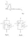
- the component of this document has the characteristic illustrated in figure 1. As long as the voltage across its terminals is lower at a cut-off voltage VD, the current is limited to a substantially constant Ion value. As soon as the voltage at component terminals exceeds the value VD, the current drops to a low Ioff value in front of Ion, from which it follows that the current in the circuit including the component is substantially interrupted.
- the component of FIG. 2A is intended to be connected between terminals A and K, terminal A or anode terminal being positive with respect to terminal K or cathode terminal. he comprises, between these terminals, a current limiter 1 and a detector voltage detector 2.
- the voltage detector is for example a voltage divider which supplies a terminal on a terminal C VC command when the voltage between terminals A and K reaches the VD disjunction value.
- the voltage VC controls the limiter current 1 to inhibit its functioning, i.e. to return it blocker.
- the voltage detector 2 causes the opening of a switch 3, in series with limiter 1, when the voltage between terminals A and K reaches the value VD.
- this detector consists of a voltage divider 2 comprising two transistors Depletion N-channel MOS connected in series and operating as nonlinear resistors. Each of these transistors MOS has its grid connected to its source.
- the extinction current Ioff corresponds essentially to the current in detector 2.
- This non-zero extinction current is often not a disadvantage for the function sought, provided that it is quite weak because it can in particular be used as detection signal after tripping of the circuit breaker.
- an object of the present invention is to achieve a current limiting monolithic static component and circuit breaker which has a very high series impedance in the state of disjunction.
- a static microdisjunction component self-locking comprising a first depletion MOS transistor of a first type connected by its drain to a first terminal main and by its grid to a second main terminal, a second complementary depletion MOS transistor connected by its drain to the second main terminal and by its source to source of the first transistor, and a third depletion MOS transistor of the first type connected by its drain at the first main terminal, by its grid at the second terminal main, and by its source to the gate of the second transistor.
- the first and third depletion MOS transistors are of the type IGBTs.
- the component further comprises a Zener diode connected between gate and drain of the second transistor.
- the first and third MOS transistors are of the vertical type and the second of lateral type.
- the component is produced in a type N silicon substrate.
- the limiter, detector and circuit breaker functions are nested in the same components, the threshold of disjunction being determined by a MOS transistor threshold voltage.
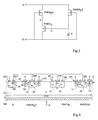
- a component according to the present invention implements the circuit illustrated in Figure 3 which is intended to be connected to two terminals A and K, terminal A being positive with respect to the terminal K.
- Two N-channel depletion MOS transistors NMOS D 1 and NMOS D 2 have their drains connected to terminal A and their gates connected to terminal K.
- a P-channel MOS transistor PMOS D has its source connected to the source of the NMOS transistor D 1, its gate connected to the source of the NMOS transistor D 2 and its drain connected to the terminal K.
- the substrate of the PMOS transistor D is floating, which makes it possible, during its conduction and blocking phases, to set its potential at neighborhood of the drain voltage thanks to the self-shielding phenomenon obtained in an integrated structure of multicell MOS type.
- the NMOS transistor D 1 has its source connected to its gate via the PMOS transistor D and that the PMOS transistor D has its gate connected to its source via the NMOS D 2 and NMOS transistors. D 1.
- the depletion transistors NMOS D 1 and PMOS D operate as two resistors of low value in series and the current increases in proportion to the voltage until reaching a value Ion.
- one or other of the NMOS D 1 and PMOS D transistors enters saturation and limits the value of the current to the Ion value mentioned above.
- NMOS transistor D 2 In a third phase, we pass to a state of disjunction. Then, the NMOS transistor D 2 is blocked in turn. To explain the entry into the disjunction phase, we must distinguish the case where the NMOS transistor D 1 enters the first in saturation from the case where the PMOS transistor D enters the first in saturation. For a given circuit breaker, this choice is made during the design stage by adjusting the physical and technological parameters of the channel region of these two devices.
- the NMOS transistor D 1 enters the first in saturation
- the voltage VA continues to increase
- the potential VG on the gate of the PMOS transistor D (which is substantially equal to the potential of terminal A the fact that the NMOS transistor D 2 is a depletion transistor which is conductive at this time) becomes greater than the threshold voltage defined between the gate and the substrate of this transistor.
- the substrate voltage is, under these conditions, close to the drain voltage (point K).
- point K the drain voltage
- the source-drain voltage then increases causing the potential of point S to increase.
- the voltage of this point S becomes greater than the threshold voltage of the NMOS transistor D 1, the latter in turn turns off.
- the anode-cathode voltage continues to increase and the potential of the source of the NMOS transistor D 2 follows this value (minus the voltage drop in this transistor).
- the NMOS transistor D 2 turns off in turn when the source-gate voltage applied to it becomes equal to its threshold voltage. It is clear that the threshold voltage of the NMOS transistor D 2 must be higher than that of the other two transistors. In this configuration, the three transistors are in the off state and, in principle, no leakage current flows through the circuit breaker.
- the PMOS transistor D enters the first in saturation
- the potential VS on the source S of the NMOS transistor D 1 becomes greater than the gate potential of this transistor.
- the difference exceeds the threshold voltage of this NMOS transistor D 1 the latter is blocked.
- the voltage VAK continues to increase, the potential of the point G also increases, and the PMOS transistor D is blocked in its turn for the same reasons as previously.
- the NMOS D 1 and PMOS D transistors are blocked and the NMOS D 2 transistor in turn is blocked because the voltage VAK continues to increase and the source potential of the NMOS D 2 transistor reaches a value such that its source-gate voltage becomes equal then higher than its threshold voltage.
- the precautions previously taken at the level of the threshold voltages and of the envisaged protections remain essential.
- circuit according to the present invention is susceptible to various variants and modifications which will appear to those skilled in the art. In particular, the latter will understand that the operation of the circuit remains the same if the NMOS D 1 and NMOS D 2 transistors are replaced by IGBT transistors.
- FIG. 4 represents an example of a monolithic embodiment of the circuit of figure 3.
- Figure 4 constituting a view in section of semiconductor component is not to scale.
- Those skilled in the art will refer to their general knowledge for determining the thicknesses and doping levels of various layers.
- the surfaces occupied by these various layers or the number of cells constituting an elementary component will, in known manner, chosen according to the technology used and power dissipation requirements.
- the distances between the various P boxes will be optimized so to provide a self-shielding effect.
- FIG 4 there is shown in a conventional and very schematic manner, respectively from right to left, a cell of a vertical MOS transistor constituting the NMOS transistor D 1, a lateral MOS transistor constituting the PMOS transistor D , a cell of a vertical MOS transistor constituting the NMOS transistor D 2, and a Zener diode Z.
- the vertical MOS transistor NMOS D 1 is formed in a low-doping type N silicon wafer 11 comprising on the side of its rear face a heavily doped layer N type 12 allowing the production of an ohmic contact with a metallization d 'anode M1 covering the rear face.
- the NMOS transistor D 1 comprises one or more cells, each of which is formed in a lightly doped P-type box 14, for example having a hexagonal or square shape when viewed from above.
- an N + type region 15 having substantially a ring shape.
- the upper part of the box 14 between the outer periphery of the ring 15 and the external periphery of the box 14 is occupied by a lightly doped N-type region 16 coated with a gate insulator 17.
- the central part of the box 14 generally corresponds to a more heavily doped P type region 18.
- the upper surface of region 18 and at least part of the ring 15 is coated with a metallization M2.
- the gate insulator 17 is coated with a metallization M3.
- M1 metallization on the rear face corresponds to the drain of the MOS transistor, connected to terminal A, and the metallization M2 constitutes, above region 15, the source contact and, above region 18, the substrate contact.
- the NMOS transistor D 2 is produced like the NMOS transistor D 1 and comprises regions 24 to 28 corresponding respectively to regions 14 to 18 and metallizations M4 and M5 corresponding respectively to metallizations M2 and M3.
- the NMOS transistor D 2 which does not have the function of allowing current to pass through will have a surface much smaller than that of the NMOS transistor D 1.
- the heavily doped N type rear semiconductor layer 12 can be replaced by a heavily doped P type layer.
- IGBT insulated gate bipolar transistors
- IGBT D insulated gate bipolar transistors
- the PMOS lateral transistor D comprises two highly doped P-type diffused regions 31 and 32 separated by a weakly doped P-type region 33 (channel region).
- Metallizations M6 and M7 are respectively formed on regions 31 and 32 and a gate metallization M8 is formed above the channel region (with the interposition of an insulating layer).
- the Zener diode Z can consist of an N + 41 region formed in a P + 42 box, the region 41 being coated with a metallization M11 and the region 42 with a metallization M12.
- Metallizations M2 and M6 are connected to each other and correspond to the connection of the sources of the NMOS D 1 and PMOS D transistors.
- the metallizations M8, M4 and M11 are interconnected and correspond to the connection of the gate of the PMOS transistor D to the source of the NMOS transistor D 2 and to the cathode of the Zener diode Z.
- the other metallizations are connected to the terminal K, as this is indicated by an arrow.
- This structure can be formed from a slice of type N silicon in a plane ⁇ 100> having a resistance of layer of 30 ohm.cm.
- Cs at / cm 3
- xj the following parameters can be chosen for the various regions.
- the thicknesses of grids can be of the order of 50 nm.
- the horizontal dimensions of the boxes are those commonly chosen in the field of MOS transistors from power, that is to say of the order of 25 to 50 ⁇ m.
- devices are obtained supporting voltages from 600 to 1500 V, whose Ion current is from 1 to 5 A and whose Ioff current is practically zero.
Landscapes
- Engineering & Computer Science (AREA)
- Power Engineering (AREA)
- Metal-Oxide And Bipolar Metal-Oxide Semiconductor Integrated Circuits (AREA)
- Insulated Gate Type Field-Effect Transistor (AREA)
Claims (5)
- Statisches selbsthaltendes Mikroschalterelement,
dadurch gekennzeichnet, dass es aufweist:einen ersten MOS-Transistor vom Verarmungstyp (NMOSD1) eines ersten Types, der über seine Drain-Elektrode mit einem ersten Hauptanschluss (A) und über seine Gate-Elektrode mit einem zweiten Hauptanschluss (K) verbunden ist,einen zweiten MOS-Transistor vom Verarmungstyp (PMOSD) Index) D vom komplementären Typ, der über seine Drain-Elektrode mit dem zweiten Hauptanschluss und über seine Source-Elektrode mit der Source-Elektrode des ersten Transistors verbunden ist, undeinen dritten MOS-Transistor vom Verarmungstyp (NMOSD2) des ersten Types, der über seine Drain-Elektrode mit dem ersten Hauptanschluss (A), über seine Gate-Elektrode mit dem zweiten Hauptanschluss (K) und über seine Source-Elektrode mit der Gate-Eelektrode des zweiten Transistors verbunden ist. - Element nach Anspruch 1, dadurch gekennzeichnet, dass der erste und der dritte MOS-Transistor vom Verarmungstyp vom Typ IGBT sind.
- Element nach Anspruch 1, dadurch gekennzeichnet, dass es darüber hinaus eine Zenerdiode aufweist, die zwischen der Gate-Elektrode und der Drain-Elektrode des zweiten Transistors verbunden ist.
- Element nach Anspruch 1, dadurch gekennzeichnet, dass der erste und der dritte MOS-Transistor vom vertikalen Typ und der zweite Transistor vom lateralen Typ sind.
- Element nach Anspruch 4, dadurch gekennzeichnet, dass es in einem Siliziumsubstrat vom Typ N realisiert ist.
Applications Claiming Priority (2)
| Application Number | Priority Date | Filing Date | Title |
|---|---|---|---|
| FR9609132 | 1996-07-16 | ||
| FR9609132A FR2751489B1 (fr) | 1996-07-16 | 1996-07-16 | Microdisjoncteur statique autoblocable |
Publications (2)
| Publication Number | Publication Date |
|---|---|
| EP0820135A1 EP0820135A1 (de) | 1998-01-21 |
| EP0820135B1 true EP0820135B1 (de) | 2002-09-25 |
Family
ID=9494278
Family Applications (1)
| Application Number | Title | Priority Date | Filing Date |
|---|---|---|---|
| EP97410072A Expired - Lifetime EP0820135B1 (de) | 1996-07-16 | 1997-07-09 | Statischer selbsthaltender Mikroschalter |
Country Status (4)
| Country | Link |
|---|---|
| US (1) | US6107664A (de) |
| EP (1) | EP0820135B1 (de) |
| DE (1) | DE69715746T2 (de) |
| FR (1) | FR2751489B1 (de) |
Families Citing this family (6)
| Publication number | Priority date | Publication date | Assignee | Title |
|---|---|---|---|---|
| US6271067B1 (en) | 1998-02-27 | 2001-08-07 | Micron Technology, Inc. | Methods of forming field effect transistors and field effect transistor circuitry |
| JP3660566B2 (ja) * | 2000-06-30 | 2005-06-15 | 新電元工業株式会社 | 過電流制限型半導体素子 |
| US20020125507A1 (en) * | 2001-03-07 | 2002-09-12 | Washburn James Ray | Interruptable high-voltage current limiter suitable for monolithic integration |
| US6900093B2 (en) * | 2003-05-16 | 2005-05-31 | Jlj, Inc. | Method of fabricating a zener diode chip for use as a shunt in Christmas tree lighting |
| EP2200141B1 (de) | 2008-12-18 | 2011-10-12 | Siemens Aktiengesellschaft | Schaltungsanordnung zum Schutz eines elektrischen Verbrauchers |
| CN120786951A (zh) * | 2025-09-09 | 2025-10-14 | 深圳平湖实验室 | 固态断路器 |
Family Cites Families (5)
| Publication number | Priority date | Publication date | Assignee | Title |
|---|---|---|---|---|
| US5128823A (en) * | 1989-06-14 | 1992-07-07 | Nippondenso Co., Ltd. | Power semiconductor apparatus |
| FR2649828B1 (fr) * | 1989-07-17 | 1991-10-31 | Sgs Thomson Microelectronics | Circuit integre vdmos/logique comprenant un transistor vertical deplete et une diode zener |
| US5696659A (en) * | 1993-02-10 | 1997-12-09 | Maruo; Masaya | Overcurrent protective circuit and semiconductor device |
| DE69415958T2 (de) * | 1994-03-29 | 1999-05-27 | Stmicroelectronics S.R.L., Agrate Brianza, Mailand/Milano | Leistungsendstufe mit begrenzter Stromsenkung während Hochimpedanzphase |
| EP0766395A3 (de) * | 1995-09-27 | 1999-04-21 | Siemens Aktiengesellschaft | Leistungstransistor mit Kurzschlussschutz |
-
1996
- 1996-07-16 FR FR9609132A patent/FR2751489B1/fr not_active Expired - Fee Related
-
1997
- 1997-07-09 EP EP97410072A patent/EP0820135B1/de not_active Expired - Lifetime
- 1997-07-09 DE DE69715746T patent/DE69715746T2/de not_active Expired - Fee Related
- 1997-07-14 US US08/891,774 patent/US6107664A/en not_active Expired - Lifetime
Also Published As
| Publication number | Publication date |
|---|---|
| US6107664A (en) | 2000-08-22 |
| DE69715746D1 (de) | 2002-10-31 |
| FR2751489A1 (fr) | 1998-01-23 |
| DE69715746T2 (de) | 2003-05-22 |
| FR2751489B1 (fr) | 1998-10-16 |
| EP0820135A1 (de) | 1998-01-21 |
Similar Documents
| Publication | Publication Date | Title |
|---|---|---|
| EP0579561B1 (de) | Schutzschaltung gegen Überspannungen für Leistungsbauteil | |
| EP0543742B1 (de) | Monolithische Niederspannungsschutzdiode mit geringer Kapazität | |
| FR2812972A1 (fr) | Dispositif a semiconducteur consistant en un thyristor pour la protection contre les decharges electrostatiques | |
| EP0742591B1 (de) | Bauelement für den vollständigen Schutz einer Schnittstellenschaltung von Teilnehmerleitungen | |
| EP0583203B1 (de) | Schaltung zum Ziehen des Eingangs einer integrierten Schaltung auf einen definierten Zustand | |
| FR2698486A1 (fr) | Structure de protection contre les surtensions directes pour composant semiconducteur vertical. | |
| EP0780952B1 (de) | Monolithischer und statischer Strombegrenzer und Schutzschalter | |
| EP0820135B1 (de) | Statischer selbsthaltender Mikroschalter | |
| FR2762445A1 (fr) | Composant de protection d'interface de lignes telephoniques | |
| EP0652598A2 (de) | Spannungsgesteuerter bidirectionaler Schalter | |
| EP1076365B1 (de) | Empfindlicher statischer Zweirichtungsschalter | |
| EP0881682B1 (de) | Hochspannungsschutzanordnung für einen integrierten MOS-Leistungstransistor | |
| EP0865671B1 (de) | Normal leitender dual-thyristor | |
| EP0624943A1 (de) | Seriengeschaltetes Strombegrenzerbauelement | |
| EP0599739B1 (de) | Thyristor und Aufbau von Thyristoren mit gemeinsamer Katode | |
| FR2773021A1 (fr) | Commutateur bidirectionnel normalement ferme | |
| FR2818805A1 (fr) | Commutateur statique bidirectionnel sensible | |
| EP0704903B1 (de) | Halbleitervorrichtung zur Speisung, Rückleitung und Entmagnetisierung einer induktiven Last | |
| EP0881681B1 (de) | Anordnung zum Schützen einer integrierten MOS-Vorrichtung gegen Spannungsabfälle | |
| EP3091572B1 (de) | Bidirektioneller leistungsschalter | |
| EP0929140B1 (de) | Schutz eines vertikalen, Messzellen zugeordneten MOS-Transistors | |
| FR2764735A1 (fr) | Protection du caisson logique d'un composant incluant un transistor mos de puissance integre | |
| FR2993402A1 (fr) | Circuit integre sur soi comprenant une diode laterale de protection contre des decharges electrostatiques | |
| EP2246886A1 (de) | Integrierter Schaltkreis, der mit einem großflächigen Schutz gegen elektrostatische Entladungen ausgestattet ist | |
| FR2904473A1 (fr) | Dispositif de protection d'un circuit integre contre les decharges electrostatiques |
Legal Events
| Date | Code | Title | Description |
|---|---|---|---|
| PUAI | Public reference made under article 153(3) epc to a published international application that has entered the european phase |
Free format text: ORIGINAL CODE: 0009012 |
|
| AK | Designated contracting states |
Kind code of ref document: A1 Designated state(s): DE FR GB IT |
|
| 17P | Request for examination filed |
Effective date: 19980625 |
|
| AKX | Designation fees paid |
Free format text: DE FR GB IT |
|
| RBV | Designated contracting states (corrected) |
Designated state(s): DE FR GB IT |
|
| RAP3 | Party data changed (applicant data changed or rights of an application transferred) |
Owner name: STMICROELECTRONICS S.A. |
|
| GRAG | Despatch of communication of intention to grant |
Free format text: ORIGINAL CODE: EPIDOS AGRA |
|
| 17Q | First examination report despatched |
Effective date: 20010928 |
|
| RIC1 | Information provided on ipc code assigned before grant |
Free format text: 7H 02H 9/02 A, 7H 01L 27/06 B |
|
| RAP1 | Party data changed (applicant data changed or rights of an application transferred) |
Owner name: STMICROELECTRONICS S.A. |
|
| GRAG | Despatch of communication of intention to grant |
Free format text: ORIGINAL CODE: EPIDOS AGRA |
|
| GRAH | Despatch of communication of intention to grant a patent |
Free format text: ORIGINAL CODE: EPIDOS IGRA |
|
| GRAH | Despatch of communication of intention to grant a patent |
Free format text: ORIGINAL CODE: EPIDOS IGRA |
|
| GRAA | (expected) grant |
Free format text: ORIGINAL CODE: 0009210 |
|
| AK | Designated contracting states |
Kind code of ref document: B1 Designated state(s): DE FR GB IT |
|
| PG25 | Lapsed in a contracting state [announced via postgrant information from national office to epo] |
Ref country code: IT Free format text: LAPSE BECAUSE OF FAILURE TO SUBMIT A TRANSLATION OF THE DESCRIPTION OR TO PAY THE FEE WITHIN THE PRESCRIBED TIME-LIMIT;WARNING: LAPSES OF ITALIAN PATENTS WITH EFFECTIVE DATE BEFORE 2007 MAY HAVE OCCURRED AT ANY TIME BEFORE 2007. THE CORRECT EFFECTIVE DATE MAY BE DIFFERENT FROM THE ONE RECORDED. Effective date: 20020925 |
|
| REG | Reference to a national code |
Ref country code: GB Ref legal event code: FG4D Free format text: NOT ENGLISH |
|
| REF | Corresponds to: |
Ref document number: 69715746 Country of ref document: DE Date of ref document: 20021031 |
|
| GBT | Gb: translation of ep patent filed (gb section 77(6)(a)/1977) |
Effective date: 20030113 |
|
| PLBE | No opposition filed within time limit |
Free format text: ORIGINAL CODE: 0009261 |
|
| STAA | Information on the status of an ep patent application or granted ep patent |
Free format text: STATUS: NO OPPOSITION FILED WITHIN TIME LIMIT |
|
| 26N | No opposition filed |
Effective date: 20030626 |
|
| PGFP | Annual fee paid to national office [announced via postgrant information from national office to epo] |
Ref country code: GB Payment date: 20050706 Year of fee payment: 9 |
|
| PGFP | Annual fee paid to national office [announced via postgrant information from national office to epo] |
Ref country code: DE Payment date: 20050707 Year of fee payment: 9 |
|
| PGFP | Annual fee paid to national office [announced via postgrant information from national office to epo] |
Ref country code: FR Payment date: 20050708 Year of fee payment: 9 |
|
| PG25 | Lapsed in a contracting state [announced via postgrant information from national office to epo] |
Ref country code: GB Free format text: LAPSE BECAUSE OF NON-PAYMENT OF DUE FEES Effective date: 20060709 |
|
| PG25 | Lapsed in a contracting state [announced via postgrant information from national office to epo] |
Ref country code: DE Free format text: LAPSE BECAUSE OF NON-PAYMENT OF DUE FEES Effective date: 20070201 |
|
| GBPC | Gb: european patent ceased through non-payment of renewal fee |
Effective date: 20060709 |
|
| REG | Reference to a national code |
Ref country code: FR Ref legal event code: ST Effective date: 20070330 |
|
| PG25 | Lapsed in a contracting state [announced via postgrant information from national office to epo] |
Ref country code: FR Free format text: LAPSE BECAUSE OF NON-PAYMENT OF DUE FEES Effective date: 20060731 |