EP0929140B1 - Schutz eines vertikalen, Messzellen zugeordneten MOS-Transistors - Google Patents
Schutz eines vertikalen, Messzellen zugeordneten MOS-Transistors Download PDFInfo
- Publication number
- EP0929140B1 EP0929140B1 EP98410154A EP98410154A EP0929140B1 EP 0929140 B1 EP0929140 B1 EP 0929140B1 EP 98410154 A EP98410154 A EP 98410154A EP 98410154 A EP98410154 A EP 98410154A EP 0929140 B1 EP0929140 B1 EP 0929140B1
- Authority
- EP
- European Patent Office
- Prior art keywords
- transistor
- source
- short
- cells
- circuiting
- Prior art date
- Legal status (The legal status is an assumption and is not a legal conclusion. Google has not performed a legal analysis and makes no representation as to the accuracy of the status listed.)
- Expired - Lifetime
Links
Images



Classifications
-
- H—ELECTRICITY
- H03—ELECTRONIC CIRCUITRY
- H03K—PULSE TECHNIQUE
- H03K17/00—Electronic switching or gating, i.e. not by contact-making and –breaking
- H03K17/08—Modifications for protecting switching circuit against overcurrent or overvoltage
- H03K17/081—Modifications for protecting switching circuit against overcurrent or overvoltage without feedback from the output circuit to the control circuit
- H03K17/0814—Modifications for protecting switching circuit against overcurrent or overvoltage without feedback from the output circuit to the control circuit by measures taken in the output circuit
- H03K17/08142—Modifications for protecting switching circuit against overcurrent or overvoltage without feedback from the output circuit to the control circuit by measures taken in the output circuit in field-effect transistor switches
-
- H—ELECTRICITY
- H10—SEMICONDUCTOR DEVICES; ELECTRIC SOLID-STATE DEVICES NOT OTHERWISE PROVIDED FOR
- H10D—INORGANIC ELECTRIC SEMICONDUCTOR DEVICES
- H10D89/00—Aspects of integrated devices not covered by groups H10D84/00 - H10D88/00
- H10D89/60—Integrated devices comprising arrangements for electrical or thermal protection, e.g. protection circuits against electrostatic discharge [ESD]
- H10D89/601—Integrated devices comprising arrangements for electrical or thermal protection, e.g. protection circuits against electrostatic discharge [ESD] for devices having insulated gate electrodes, e.g. for IGFETs or IGBTs
-
- H—ELECTRICITY
- H10—SEMICONDUCTOR DEVICES; ELECTRIC SOLID-STATE DEVICES NOT OTHERWISE PROVIDED FOR
- H10D—INORGANIC ELECTRIC SEMICONDUCTOR DEVICES
- H10D89/00—Aspects of integrated devices not covered by groups H10D84/00 - H10D88/00
- H10D89/60—Integrated devices comprising arrangements for electrical or thermal protection, e.g. protection circuits against electrostatic discharge [ESD]
- H10D89/601—Integrated devices comprising arrangements for electrical or thermal protection, e.g. protection circuits against electrostatic discharge [ESD] for devices having insulated gate electrodes, e.g. for IGFETs or IGBTs
- H10D89/811—Integrated devices comprising arrangements for electrical or thermal protection, e.g. protection circuits against electrostatic discharge [ESD] for devices having insulated gate electrodes, e.g. for IGFETs or IGBTs using FETs as protective elements
Definitions
- the present invention relates to vertical power MOS transistors and more particularly to the protection of a vertical power MOS transistor coupled to a vertical MOS current measurement transistor.
- a vertical power MOS transistor generally consists of a large number of identical elementary cells in parallel. To measure the current in this transistor it is customary to associate a measurement transistor made up of a smaller number of the same elementary cells, subjected to the same polarization conditions. This is for example described in the documents WO-A-89/08928 and US Patent 5410171 .
- the load of the power transistor is an inductive load, a negative voltage appears across the load when opening the power transistor. This voltage is likely to trigger the conduction of parasitic elements and damage the power transistor.
- the figure 1 represents a circuit comprising a vertical MOS transistor of power T1 composed of n elementary cells T11 to T1n, associated with a vertical measurement MOS transistor T2 comprising m elementary cells T21 to T2m with m much smaller than n.
- the drains D of the elementary cells of the power transistor and of the measurement transistor are connected together to a potential Vcc power purpose.
- the gates G of the elementary cells of the power transistor and of the measurement transistor are connected together to a control terminal G.
- the sources S1 of the elementary cells of the power transistor are interconnected and connected by an inductive load L to ground.
- the sources S2 of the elementary cells of the measurement transistor are interconnected and connected to a current source I ref .
- the voltage difference between the terminals S1 and S2 gives an indication that the current in the power transistor is greater than or less than a threshold equal to (n / m) I ref .
- the current source Iref can be replaced by a resistor R, when the circuit is intended to measure a load resistance instead of a load current.
- the figure 2 schematically represents a vertical sectional view of a portion of a silicon wafer 2 in which are formed the transistors T1 and T2.
- the drain of an elementary cell corresponds to the substrate 21 of the wafer.
- the zone 21 is connected via a zone 20 of highly doped N (N + ) type to a metallization 22 connected to the drain terminal D of the circuit of the figure 1 .
- the source of an elementary cell corresponds to an N + type ring 25 formed in a P type box 23.
- the box 23 generally comprises a P-type (P + ) strongly doped central zone 24.
- a source metallization 26 is in contact with the central part of each box 23 and with the ring 25.
- the gate of an elementary cell is formed by a polycrystalline silicon layer 27, isolated from the surface of the wafer by a dielectric, which covers a channel zone between the outer periphery of the ring 25 and the outer periphery of the box. 23.
- the grids 27 are interconnected to a gate node G.
- the figure 3 represents on a larger scale part of the figure 2 on which parasitic elements existing between two adjacent elementary cells are shown.
- the gate 27 also covers the area of the substrate 21 between two elementary cells.
- This metallization, isolated from the substrate 21, corresponds to a gate of a parasitic transistor T3 of the PMOS type formed of a P type box 23 of a first elementary cell, a substrate portion 21 of the N type and a second box 33 of type P of a second elementary cell.
- the combination of an N + type zone 25, a P type box 23 and N-type lightly doped substrate 21 forms a bipolar NPN type parasitic transistor whose emitter is the zone 25, the collector zone 21 and the base the caisson 23.
- An NPN type bipolar transistor T4 is connected between the source S1 and the drain D of the cell of the transistor T1.
- the base of transistor T4 is connected to the drain of a parasitic PMOS transistor T3.
- an NPN-type bipolar transistor T5 is connected between the source S2 and the drain D of the cell of the transistor T2, the base of the transistor T5 is connected to the source of the MOS transistor T3.
- the MOS transistor T3 is controlled by the gate G common to the transistors T1 and T2.
- the load L of the transistor T1 is an inductive load
- the voltage across the load that is to say on the source S1
- the gate G which corresponds to the gate of the transistor T3
- the MOS transistor T3 which is then conducting passes a large current between the terminals S2 and S1.
- this current which circulates in particular in the region N + 25 exceeds a certain threshold
- the bipolar transistor T4 becomes conducting. This creates a short circuit between the source 26 and drain 22 terminals of the T2i cell.
- the terminal 26 being at a very negative potential and the terminal 22 at the potential Vcc, it can result in a destructive breakdown of the structure.
- the current flowing through transistor T4 depends on the gain of this transistor. However, in the context of modern technologies, the size of the caissons 23 decreases and the doping level of the zones 24 is reduced. As a result, the gain of parasitic bipolar transistors T4 increases and thus the risk of destructive breakdown increases.
- the inventors have therefore sought ways to eliminate the destructive effects associated with the conduction of parasitic bipolar transistors by the aforementioned parasitic MOS transistors.
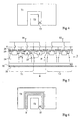
- the figure 4 schematically represents a view from above of a device such as that represented in FIG. figure 1 .
- the block T1 represents the area occupied by the elementary cells of the power transistor T1 and the block T2 represents the area occupied by the elementary cells of the measurement transistor T2.
- T3 symbolizes the parasitic MOS transistors existing between the adjacent cells of the power transistor and the measurement transistor.
- the figure 5 represents a vertical sectional view of a first solution to avoid the aforementioned destructive breakdowns.
- the structure is very close to the structure represented in figure 2 , and the same references designate the same elements.
- a buffer cell B can be implemented by suppressing the N + implantation of the sources in an elementary cell of T1. There is no longer any parasitic bipolar transistors.
- the figure 6 schematically represents a view from above of a device such as that of the figure 5 .
- the block T1 represents the area occupied by the elementary cells of the power transistor T1
- the block T2 represents the area occupied by the elementary cells of the measurement transistor T2
- the block B represents the area occupied by the buffer cells placed between the transistor of power and the measuring transistor.
- the transistor T3 represents the parasitic MOS transistors existing between the elementary cells of the measuring transistor T2 and the adjacent buffer cells B.
- An object of the present invention is to provide protection for a device such as that represented in FIG. figure 1 .
- An object of the present invention is to provide a device comprising a power transistor and a measurement transistor in which there is in normal operation a constant ratio between the current flowing through the measurement transistor and the current flowing through the power transistor.
- Another object of the present invention is to propose a solution that can be expensive and easy to implement to the problems encountered in the prior art.
- the means of short-circuiting is a MOS transistor.
- control means is a divider bridge connected across the inductive load.
- the control means consists of a diode whose anode is connected to the gate of the short-circuiting transistor and whose cathode is connected to the cathode of an avalanche diode , whose anode is connected to the source of the power transistor, and a resistor connected between the gate of the short-circuiting transistor and the ground.
- the substrate and the source of the short-circuiting transistor are connected to each other.
- the short-circuiting means is a lateral transistor. realized in the same monolithic component as the vertical power and measurement transistors.
- the figure 7 represents a simplified diagram of a circuit according to the present invention.
- a cell T1i is represented among the n elementary cells T11 to T1n of a power transistor T1, and an elementary cell T2j among the m elementary cells T21 to T2m of a measurement transistor, the cell T1i being adjacent to the cell. t2j.
- the drains of the elementary cells T1i and T2j are connected to a terminal D common to all the cells, itself connected to a high supply potential Vcc.
- Grids G of cells T1i and T2j are connected together to a control terminal G common to all the cells.
- the source of the cell T1i is connected to a terminal S1 common to all the cells of the power transistor T1, itself connected to ground by an inductive load L.
- the source of the cell T2j is connected to a terminal S2 common to all the cells of the measuring transistor T2, itself connected to a current source I ref .
- the voltage difference between terminals S1 and S2 gives an indication that the current in the power transistor is greater than or less than a threshold equal to (n / m) I ref .
- a resistor is conventionally put in series with the current source I ref , for example to limit the current in T3 when driving, and to drop the voltage on S2 when S1 becomes negative. This makes it possible to limit the voltage V GS2 of T2 when S1 and G become negative and thus to avoid a breakdown of the gate oxide of T2.
- FIG. 7 We also represented figure 7 parasitic transistors which are associated with the cells T1i and T2j.
- a bipolar parasitic transistor T4 is connected in parallel on the cell T1i.
- a bipolar parasitic transistor T5 is connected in parallel on the cell T2j.
- the bases of the transistors T4 and T5 are respectively connected to the drain and to the source of a parasitic MOS transistor T3.
- the gate of the parasitic MOS transistor T3 is connected to the gate G of the circuit.
- a short-circuiting means T6 is connected between the common source terminals S1 and S2.
- the short-circuiting means T6 is controlled by a control means C which is capable of putting the means T6 in conduction at the opening of the power transistor T1.
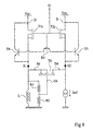
- the figure 8 discloses an embodiment of the short-circuiting means T6 and the control means C.
- the short-circuiting means is an MOS transistor T6 whose source S6 is connected to the source terminal S1 and whose drain D6 is connected to source terminal S2.
- Two resistors R1 and R2 are connected in series across the load L, the point of connection of these two resistors is connected to the gate G6 of the transistor T6.
- the resistors R1 and R2 form a divider bridge connected to the terminals of the load L.
- the resistors R1 and R2 are chosen to trigger the conduction of the transistor T6 when the power transistor T1 is open, and the voltage across the load L exceeds a predetermined negative threshold.
- This predetermined negative threshold may, for example, be chosen greater than the negative threshold for which the current flowing through the above-mentioned parasitic elements is capable of triggering the parasitic transistor T4.
- the transistor T6 When it is turned on, the transistor T6 bypasses the source terminals S1 and S2 of the circuit and eliminates any risk of crossing the parasitic MOS transistor T3 and thus conduction of the parasitic bipolar transistor T4. This avoids any risk of breakdown of the structure.
- the voltage across the load L is such that the transistor T6 remains off, so the present invention does not affect normal mode operation.
- the figure 9 represents a simplified sectional view of a part of the circuit according to the present invention.
- the right part of the circuit illustrates vertical MOS transistor cells T1 and T2 described in connection with the figure 2 .
- a short-circuiting transistor T6 in the form of a lateral-type MOS transistor.
- the drain of the transistor T6 consists of a strongly doped zone 40 of the N + type formed in a doped box 42 of the P type.
- the drain D6 of the transistor T6 is connected to the source terminal S2 of the measurement transistor.
- the source of the transistor T6 consists of a strongly doped zone 41 of N + type formed in the box 42.
- the source S6 of the transistor T6 is connected to the source terminal S1 of the power transistor.
- the casing 42 is polarized by a highly doped zone P + type, also formed in the box 42, and connected to the terminal S1.
- the gate G6 of the transistor T6 is formed by a polycrystalline silicon layer 44 situated above the section of the box 42 between the zones 40 and 41, isolated from the surface of the box 42 by a dielectric.
- the figure 10 represents a simplified top view of a circuit according to the present invention.
- the transistor T6 has been implanted in the vicinity of the transistors T1 and T2.
- the respective sizes of the transistors T1, T2, T6 are determined as a function of the maximum currents that must pass through them.
- the short-circuiting transistor T6 is, as we have seen previously, blocked in normal operating mode.
- the ratio between the currents passing through the power transistor T1 and the measurement transistor T2 remains constant and determined (equal to n / m as has been described in connection with FIG. figure 1 ).
- the present invention thus makes it possible to protect the device described in the prior art while maintaining the same ratio between measuring current and current in a power transistor.
- the addition of transistor T6 is moreover inexpensive and simple to implement.
- the short-circuiting means T6 can be realized by other structures than a MOS transistor, for example a bipolar transistor or a thyristor.
- the means of control C may be a divider bridge, but other control means fulfilling the same function may also be used.
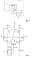
- the figure 11 represents by way of example a variant of the control means of the transistor T6.
- a circuit comprising a diode D, an avalanche diode Z and a resistor R is used here.
- the anode of the diode D is connected to a first terminal of a resistor R also connected to the gate G6 of the transistor T6, its cathode is connected to the cathode of the avalanche diode Z.
- the anode of the avalanche diode Z is connected to the source terminal S1.
- the second terminal of the resistor R is connected to ground.
- the reverse conduction voltage of the avalanche diode Z2 is chosen so that the transistor T6 is turned on when the voltage at S1 becomes more negative than a predetermined threshold.
- the control means formed by the avalanche diode Z, the diode D and the resistor R will consume less in normal operating mode than the divider bridge formed by the resistor R1 and the resistor R2 represented in FIG. figure 8 .
Landscapes
- Metal-Oxide And Bipolar Metal-Oxide Semiconductor Integrated Circuits (AREA)
- Semiconductor Integrated Circuits (AREA)
Claims (6)
- Schutzvorrichtung für ein monolithisches Bauteil, das einen diffundierten vertikalen Leistungstransistor (T1) vom MOS-Typ aufweist, welcher aus einer großen Anzahl identischer Zellen (T1i) aufgebaut ist, und einen Messtransistor (T2) aufweist, der aus einer kleineren Anzahl von Zellen (T2j) aufgebaut ist, die identisch sind zu denen des Leistungstransistors, wobei die Drain- bzw. Kollektor-Anschlüsse (D) und die Gate- bzw. Basis-Anschlüsse (G) aller Zellen gemeinsam sind, wobei eine induktive Last (L) mit dem Source- bzw. Emitter-Anschluss (S1) des Leistungstransistors verbunden ist,
dadurch gekennzeichnet, dass die Schutzvorrichtung folgendes aufweist: Kurzschlussmittel (T6), die zwischen dem Source- bzw. Emitter-Anschluss (S1) des Leistungstransistors und Source- bzw. Emitter-Anschluss (S2) des Messtransistors verbunden sind, und
Steuermittel (C), die in der Lage sind, die Kurzschlussmittel ein- bzw. durchzuschalten, wenn der Leistungstransistor abschaltet bzw. öffnet. - Schutzvorrichtung gemäß Anspruch 1, dadurch gekennzeichnet, dass die Kurzschlussmittel ein MOS-Transistor sind.
- Schutzvorrichtung gemäß Anspruch 1 oder 2, dadurch gekennzeichnet, dass die Steuermittel eine Teilerbrücke bzw. ein Spannungsteiler (R1, R2) sind, die bzw. der über die induktive Last hinweg verbunden ist.
- Schutzvorrichtung gemäß Anspruch 1 oder 2, dadurch gekennzeichnet, dass die Steuermittel bestehen aus einer Diode (D), deren Anode mit dem Gate- bzw. Basis-Anschluss (G6) des Kurzschlusstransistors verbunden ist, und deren Kathode mit der Kathode einer Zener- bzw. Durchbruch-Diode (Z) verbunden ist, wobei die Anode der Zener- bzw. Durchbruch-Diode (Z) mit dem Source- bzw. Emitter-Anschluss des Leistungstransistors verbunden ist, und aus einem Widerstand (R), der zwischen dem Gate- bzw. Basis-Anschluss (G6) des Kurzschlusstransistors und Masse verbunden ist.
- Schutzvorrichtung gemäß einem der Ansprüche 2 bis 4, dadurch gekennzeichnet, dass das Substrat und der Source- bzw. Emitter-Anschluss des Kurzschlusstransistors miteinander verbunden sind.
- Schutzvorrichtung gemäß Anspruch 2, dadurch gekennzeichnet, dass die Kurzschlussmittel (T6) ein Lateraltransistor sind, welcher in dem gleichen monolithischen Bauteil implementiert ist wie der vertikale Leistungstransistor (T1) und der vertikaler Messtransistor (T2).
Applications Claiming Priority (2)
| Application Number | Priority Date | Filing Date | Title |
|---|---|---|---|
| FR9716868 | 1997-12-31 | ||
| FR9716868A FR2773277B1 (fr) | 1997-12-31 | 1997-12-31 | Protection d'un transistor mos vertical associe a des cellules de mesure |
Publications (2)
| Publication Number | Publication Date |
|---|---|
| EP0929140A1 EP0929140A1 (de) | 1999-07-14 |
| EP0929140B1 true EP0929140B1 (de) | 2008-10-01 |
Family
ID=9515435
Family Applications (1)
| Application Number | Title | Priority Date | Filing Date |
|---|---|---|---|
| EP98410154A Expired - Lifetime EP0929140B1 (de) | 1997-12-31 | 1998-12-31 | Schutz eines vertikalen, Messzellen zugeordneten MOS-Transistors |
Country Status (4)
| Country | Link |
|---|---|
| US (1) | US6249409B1 (de) |
| EP (1) | EP0929140B1 (de) |
| DE (1) | DE69840065D1 (de) |
| FR (1) | FR2773277B1 (de) |
Families Citing this family (3)
| Publication number | Priority date | Publication date | Assignee | Title |
|---|---|---|---|---|
| JP2002171013A (ja) * | 2000-12-04 | 2002-06-14 | Sony Corp | 磁気抵抗効果素子および磁気抵抗効果型磁気ヘッド |
| DE102013107699A1 (de) * | 2013-07-18 | 2015-01-22 | Springburo GmbH | Spannungsbegrenzer |
| FR3068836B1 (fr) * | 2017-07-07 | 2019-08-23 | Stmicroelectronics (Rousset) Sas | Circuit de protection d'un commutateur de puissance |
Family Cites Families (4)
| Publication number | Priority date | Publication date | Assignee | Title |
|---|---|---|---|---|
| US4931844A (en) | 1988-03-09 | 1990-06-05 | Ixys Corporation | High power transistor with voltage, current, power, resistance, and temperature sensing capability |
| JP3175852B2 (ja) * | 1992-03-30 | 2001-06-11 | 株式会社デンソー | 半導体装置及びその製造方法 |
| US5420532A (en) * | 1993-08-20 | 1995-05-30 | Texas Instruments Incorporated | Synchronous rectifying circuit |
| DE69629278D1 (de) * | 1996-04-30 | 2003-09-04 | St Microelectronics Srl | Schaltung zum gesteuerten schwingungsfreien Rückleiten des Entladungsstromes einer induktiven Last |
-
1997
- 1997-12-31 FR FR9716868A patent/FR2773277B1/fr not_active Expired - Fee Related
-
1998
- 1998-12-15 US US09/211,772 patent/US6249409B1/en not_active Expired - Lifetime
- 1998-12-31 DE DE69840065T patent/DE69840065D1/de not_active Expired - Lifetime
- 1998-12-31 EP EP98410154A patent/EP0929140B1/de not_active Expired - Lifetime
Also Published As
| Publication number | Publication date |
|---|---|
| FR2773277A1 (fr) | 1999-07-02 |
| FR2773277B1 (fr) | 2000-03-10 |
| DE69840065D1 (de) | 2008-11-13 |
| EP0929140A1 (de) | 1999-07-14 |
| US6249409B1 (en) | 2001-06-19 |
Similar Documents
| Publication | Publication Date | Title |
|---|---|---|
| EP0579561B1 (de) | Schutzschaltung gegen Überspannungen für Leistungsbauteil | |
| EP0543742B1 (de) | Monolithische Niederspannungsschutzdiode mit geringer Kapazität | |
| EP0388329B1 (de) | Steuerschaltung für einen MOS-Leistungstransistor mit induktiver Last | |
| FR2710191A1 (fr) | MOSFET de puissance avec protection de sur-intensité et de surchauffe. | |
| EP0467799A1 (de) | Einrichtung zum Schutz gegen Überspannungen und ihre monolithische Herstellung | |
| EP0599745A1 (de) | Überspannungsschutzstruktur für vertikale Halbleiterkomponenten | |
| EP2290691A1 (de) | Schutzvorrichtung für einen integrierten Schaltkreis gegen elektrostatische Entladungen | |
| EP0742591B1 (de) | Bauelement für den vollständigen Schutz einer Schnittstellenschaltung von Teilnehmerleitungen | |
| EP0780952B1 (de) | Monolithischer und statischer Strombegrenzer und Schutzschalter | |
| FR3016999A1 (fr) | Dispositif electronique, en particulier pour la protection contre les decharges electrostatiques | |
| EP0359680B1 (de) | Integrierbare, aktive Diode | |
| EP0624943B1 (de) | Seriengeschaltetes Strombegrenzerbauelement | |
| EP0289431A1 (de) | Integrierte Schaltung, geschützt gegen Überspannungen | |
| EP0865671B1 (de) | Normal leitender dual-thyristor | |
| FR2955699A1 (fr) | Structure de protection d'un circuit integre contre des decharges electrostatiques | |
| EP0881682B1 (de) | Hochspannungsschutzanordnung für einen integrierten MOS-Leistungstransistor | |
| EP0518790A1 (de) | Bidirektionales Schutzunterteil | |
| EP0820135B1 (de) | Statischer selbsthaltender Mikroschalter | |
| EP0929140A1 (de) | Schutz eines vertikalen, Messzellen zugeordneten MOS-Transistors | |
| EP0619637B1 (de) | Schutz eines Kraftfahrzeugdrehstromgenerators | |
| EP1544919B1 (de) | Triac | |
| EP0881681B1 (de) | Anordnung zum Schützen einer integrierten MOS-Vorrichtung gegen Spannungsabfälle | |
| EP4358126A1 (de) | Elektronische vorrichtung | |
| EP4358125A1 (de) | Leistungstransistor | |
| EP0895331B1 (de) | Schutzvorrichtung für elektrische Last und Versorgungseinrichtung mit einer solchen Vorrichtung |
Legal Events
| Date | Code | Title | Description |
|---|---|---|---|
| PUAI | Public reference made under article 153(3) epc to a published international application that has entered the european phase |
Free format text: ORIGINAL CODE: 0009012 |
|
| AK | Designated contracting states |
Kind code of ref document: A1 Designated state(s): DE FR GB IT |
|
| AX | Request for extension of the european patent |
Free format text: AL;LT;LV;MK;RO;SI |
|
| 17P | Request for examination filed |
Effective date: 19991220 |
|
| AKX | Designation fees paid |
Free format text: DE FR GB IT |
|
| RAP1 | Party data changed (applicant data changed or rights of an application transferred) |
Owner name: STMICROELECTRONICS S.A. |
|
| 17Q | First examination report despatched |
Effective date: 20070919 |
|
| GRAP | Despatch of communication of intention to grant a patent |
Free format text: ORIGINAL CODE: EPIDOSNIGR1 |
|
| GRAS | Grant fee paid |
Free format text: ORIGINAL CODE: EPIDOSNIGR3 |
|
| GRAA | (expected) grant |
Free format text: ORIGINAL CODE: 0009210 |
|
| AK | Designated contracting states |
Kind code of ref document: B1 Designated state(s): DE FR GB IT |
|
| REG | Reference to a national code |
Ref country code: GB Ref legal event code: FG4D Free format text: NOT ENGLISH |
|
| REF | Corresponds to: |
Ref document number: 69840065 Country of ref document: DE Date of ref document: 20081113 Kind code of ref document: P |
|
| PLBE | No opposition filed within time limit |
Free format text: ORIGINAL CODE: 0009261 |
|
| STAA | Information on the status of an ep patent application or granted ep patent |
Free format text: STATUS: NO OPPOSITION FILED WITHIN TIME LIMIT |
|
| 26N | No opposition filed |
Effective date: 20090702 |
|
| PGFP | Annual fee paid to national office [announced via postgrant information from national office to epo] |
Ref country code: GB Payment date: 20101201 Year of fee payment: 13 Ref country code: IT Payment date: 20101127 Year of fee payment: 13 |
|
| GBPC | Gb: european patent ceased through non-payment of renewal fee |
Effective date: 20111231 |
|
| PG25 | Lapsed in a contracting state [announced via postgrant information from national office to epo] |
Ref country code: GB Free format text: LAPSE BECAUSE OF NON-PAYMENT OF DUE FEES Effective date: 20111231 |
|
| PG25 | Lapsed in a contracting state [announced via postgrant information from national office to epo] |
Ref country code: IT Free format text: LAPSE BECAUSE OF NON-PAYMENT OF DUE FEES Effective date: 20111231 |
|
| REG | Reference to a national code |
Ref country code: FR Ref legal event code: PLFP Year of fee payment: 18 |
|
| REG | Reference to a national code |
Ref country code: FR Ref legal event code: PLFP Year of fee payment: 19 |
|
| REG | Reference to a national code |
Ref country code: FR Ref legal event code: PLFP Year of fee payment: 20 |
|
| PGFP | Annual fee paid to national office [announced via postgrant information from national office to epo] |
Ref country code: FR Payment date: 20171121 Year of fee payment: 20 Ref country code: DE Payment date: 20171120 Year of fee payment: 20 |
|
| REG | Reference to a national code |
Ref country code: DE Ref legal event code: R071 Ref document number: 69840065 Country of ref document: DE |