EP0822082A2 - Tête d'enregistrement à jet d'encre, procédé de fabrication de la tête et appareil d'enregistrement à jet d'encre utilisant la tête - Google Patents
Tête d'enregistrement à jet d'encre, procédé de fabrication de la tête et appareil d'enregistrement à jet d'encre utilisant la tête Download PDFInfo
- Publication number
- EP0822082A2 EP0822082A2 EP97113150A EP97113150A EP0822082A2 EP 0822082 A2 EP0822082 A2 EP 0822082A2 EP 97113150 A EP97113150 A EP 97113150A EP 97113150 A EP97113150 A EP 97113150A EP 0822082 A2 EP0822082 A2 EP 0822082A2
- Authority
- EP
- European Patent Office
- Prior art keywords
- ink
- wiring substrate
- recording device
- substrate
- device substrate
- Prior art date
- Legal status (The legal status is an assumption and is not a legal conclusion. Google has not performed a legal analysis and makes no representation as to the accuracy of the status listed.)
- Granted
Links
Images




Classifications
-
- B—PERFORMING OPERATIONS; TRANSPORTING
- B41—PRINTING; LINING MACHINES; TYPEWRITERS; STAMPS
- B41J—TYPEWRITERS; SELECTIVE PRINTING MECHANISMS, i.e. MECHANISMS PRINTING OTHERWISE THAN FROM A FORME; CORRECTION OF TYPOGRAPHICAL ERRORS
- B41J2/00—Typewriters or selective printing mechanisms characterised by the printing or marking process for which they are designed
- B41J2/005—Typewriters or selective printing mechanisms characterised by the printing or marking process for which they are designed characterised by bringing liquid or particles selectively into contact with a printing material
- B41J2/01—Ink jet
- B41J2/135—Nozzles
- B41J2/14—Structure thereof only for on-demand ink jet heads
- B41J2/14016—Structure of bubble jet print heads
- B41J2/14072—Electrical connections, e.g. details on electrodes, connecting the chip to the outside...
-
- B—PERFORMING OPERATIONS; TRANSPORTING
- B41—PRINTING; LINING MACHINES; TYPEWRITERS; STAMPS
- B41J—TYPEWRITERS; SELECTIVE PRINTING MECHANISMS, i.e. MECHANISMS PRINTING OTHERWISE THAN FROM A FORME; CORRECTION OF TYPOGRAPHICAL ERRORS
- B41J2/00—Typewriters or selective printing mechanisms characterised by the printing or marking process for which they are designed
- B41J2/005—Typewriters or selective printing mechanisms characterised by the printing or marking process for which they are designed characterised by bringing liquid or particles selectively into contact with a printing material
- B41J2/01—Ink jet
- B41J2/135—Nozzles
- B41J2/14—Structure thereof only for on-demand ink jet heads
- B41J2/14016—Structure of bubble jet print heads
- B41J2/14024—Assembling head parts
-
- B—PERFORMING OPERATIONS; TRANSPORTING
- B41—PRINTING; LINING MACHINES; TYPEWRITERS; STAMPS
- B41J—TYPEWRITERS; SELECTIVE PRINTING MECHANISMS, i.e. MECHANISMS PRINTING OTHERWISE THAN FROM A FORME; CORRECTION OF TYPOGRAPHICAL ERRORS
- B41J2/00—Typewriters or selective printing mechanisms characterised by the printing or marking process for which they are designed
- B41J2/005—Typewriters or selective printing mechanisms characterised by the printing or marking process for which they are designed characterised by bringing liquid or particles selectively into contact with a printing material
- B41J2/01—Ink jet
- B41J2/135—Nozzles
- B41J2/16—Production of nozzles
- B41J2/1601—Production of bubble jet print heads
- B41J2/1603—Production of bubble jet print heads of the front shooter type
-
- B—PERFORMING OPERATIONS; TRANSPORTING
- B41—PRINTING; LINING MACHINES; TYPEWRITERS; STAMPS
- B41J—TYPEWRITERS; SELECTIVE PRINTING MECHANISMS, i.e. MECHANISMS PRINTING OTHERWISE THAN FROM A FORME; CORRECTION OF TYPOGRAPHICAL ERRORS
- B41J2/00—Typewriters or selective printing mechanisms characterised by the printing or marking process for which they are designed
- B41J2/005—Typewriters or selective printing mechanisms characterised by the printing or marking process for which they are designed characterised by bringing liquid or particles selectively into contact with a printing material
- B41J2/01—Ink jet
- B41J2/135—Nozzles
- B41J2/16—Production of nozzles
- B41J2/1621—Manufacturing processes
- B41J2/1623—Manufacturing processes bonding and adhesion
-
- H—ELECTRICITY
- H05—ELECTRIC TECHNIQUES NOT OTHERWISE PROVIDED FOR
- H05K—PRINTED CIRCUITS; CASINGS OR CONSTRUCTIONAL DETAILS OF ELECTRIC APPARATUS; MANUFACTURE OF ASSEMBLAGES OF ELECTRICAL COMPONENTS
- H05K3/00—Apparatus or processes for manufacturing printed circuits
- H05K3/30—Assembling printed circuits with electric components, e.g. with resistors
- H05K3/32—Assembling printed circuits with electric components, e.g. with resistors electrically connecting electric components or wires to printed circuits
- H05K3/321—Assembling printed circuits with electric components, e.g. with resistors electrically connecting electric components or wires to printed circuits by conductive adhesives
-
- H—ELECTRICITY
- H05—ELECTRIC TECHNIQUES NOT OTHERWISE PROVIDED FOR
- H05K—PRINTED CIRCUITS; CASINGS OR CONSTRUCTIONAL DETAILS OF ELECTRIC APPARATUS; MANUFACTURE OF ASSEMBLAGES OF ELECTRICAL COMPONENTS
- H05K3/00—Apparatus or processes for manufacturing printed circuits
- H05K3/36—Assembling printed circuits with other printed circuits
- H05K3/361—Assembling flexible printed circuits with other printed circuits
Definitions
- the present invention relates to a recording head of an ink-jet recording apparatus for OA machines or the like.
- the present invention relates to an ink-jet recording head comprising a recording device substrate for discharging a recording liquid fitted to a flexible film wiring substrate.
- the present invention relates also to an ink-jet recording apparatus employing the ink-jet recording head.
- the ink-jet recording apparatus which conducts recording by a non-impact recording system, has advantages of high speed recording, suitability for various recording mediums, and less recording noise generation. Therefore, the ink-jet recording is employed widely in recording mechanisms of various machines such as printers, word processors, and copying machines.
- the ink-jet recording conducts recording by discharging fine liquid droplets through a discharge opening onto a recording medium like a paper sheet, typically employing an electrothermal converting element.
- the ink-jet recording apparatus is constituted generally of an ink-jet recording head having a nozzle for forming liquid droplets and an ink-supplying system for supplying the ink to the head.
- the electrothermal converting element is provided in a pressurizing chamber.
- An electric pulse as the recording signal is applied to the electrothermal converting element to give thermal energy to the recording liquid.
- the phase change of the recording liquid due to thermal energy causes bubbling (or boiling) of the recording liquid, and the pressure of the bubbles forces the recording liquid to eject.
- the ink-jet recording heads employing the electrothermal converting system are classified into two types: an edge shooter type which discharges the recording liquid in the direction parallel to the substrate having electrothermal converting elements arranged thereon, and a side shooter type which discharges the recording liquid in the direction perpendicular to the substrate.
- the constitution of the ink-jet recording head is described specifically by reference to the side shooter type recording head.
- Fig. 10 is a perspective view of a side shooter type recording head.
- Plural discharge openings 202 are formed for discharging ink at the central portion on the front side of a recording device substrate 201.
- an ink-supplying opening 203 (broken line in the drawing) is formed in a length nearly equal to the length of the row of the discharge openings.
- electrodes on the recording device substrate 201 are electrically connected to electrode terminals of a flexible film wiring substrate 204.
- the input terminals of the flexible film wiring substrate 204 are electrically connected to output terminals of a wiring substrate 206 having external input pads 205 for supplying electric signals of recording information and the like to an ink-jet recording head from an ink-jet recording apparatus body.
- the numeral 212 indicates an ink supplying-holding member.
- Fig. 11 shows specifically a structure of the recording device substrate and the flexible film wiring substrate.
- Fig. 12A and Fig. 12B show the state of the recording device substrate fitted to the flexible film wiring substrate:
- Fig. 12A is a perspective view showing the state, and
- Fig. 12B is a sectional view taken along the plane 12B in Fig. 12A.
- electrodes 210 are formed on a recording device substrate 201 for connection with output terminals of a flexible film wiring substrate 204.
- the electrodes 210 are usually formed in rows on the end portion of the surface of the recording device substrate 201.
- the electrode formation can be conducted by a conventional technique such as plating by patterning, and ball-electrode formation by wire bonding (stud bump).
- the flexible film wiring substrate 204 has an aperture which uncovers the orifice face 207 having discharge orifices 202 when the recording device substrate 201 is fitted thereto.
- electrode terminals 208 are provided for connection with the electrodes 210 on the recording device substrate 201.
- the electrode terminals 208 of the flexible film wiring substrate 204 are connected with the electrodes 210 of the recording device substrate 201 by ILB (inner lead bonding) of the terminals of TAB (tape automated bonding).
- the recording device substrate 201 is fitted to the flexible film wiring substrate 204 as shown Figs. 12A and 12B such that the electrodes 210 of the recording device substrate 201 are connected to the electrode terminals 208 of the flexible film wiring substrate 204 and the orifice face 207 is fitted to the aperture of the flexible film wiring substrate 204.
- the electrode portions are coated and sealed with a sealing material 211 such as an epoxy resin which has sufficient sealing and ion-intercepting properties.
- the recording liquid is supplied from an ink supply opening 203 to an ink flow path 209 communicating with ink discharge openings 202, and liquid droplets are discharged through the discharge openings 202.
- an ink supplying-holding member (212 in Fig. 10) has come to be employed which holds plural flexible film wiring substrates 204 holding plural recording device substrates.
- the input terminals 204' of the flexible film wiring substrate 204 are connected to the output terminals 206' of the wiring substrate 206 by solder 213, and a flux is used as an active agent for removal of an oxide film and stains.
- the above-mentioned ink-jet recording head has problems of low printing quality and low reliability as described below.
- an ink-jet recording head comprising at least one recording device substrate for discharging a recording liquid by pressure of bubble formation caused by thermal energy, a flexible film wiring substrate for fitting the recording device substrate thereto, an electrode pad for receiving control signals from outside for controlling thermal energy generation in the recording device substrate, and a wiring substrate connected electrically to the recording device substrate with interposition of the flexible film wiring substrate, wherein an input terminal of the flexible film wiring substrate and an output terminal of the wiring substrate are electrically connected to each other and fixed by a thermosetting adhesive by hot-pressing, and the connected electrode portion is coated with the thermosetting adhesive.
- an electrode terminal of the flexible film wiring substrate and an electrode of the recording device substrate may be electrically connected to each other and fixed by a thermosetting adhesive by hot-pressing, and the connected electrode portion may be coated with the thermosetting adhesive.
- the electrode portion connected and fixed by the thermosetting adhesive may be further sealed with a sealant.
- the thermosetting adhesive may be mainly composed of an epoxy resin
- the sealant may be mainly composed of a silicone resin.
- the protrusion of the thermosetting adhesive from the edge portion of the flexible film wiring substrate may be limited, for example, to be not more than 0.5 mm.
- the above ink-jet recording head may be constructed such that the recording device substrate is held on a liquid supplying-holding member for supplying the recording liquid to the recording device substrate, and the wiring substrate is held in a face adjacent to the recording device substrate-holding face of the liquid supplying-holding member.
- the above ink-jet recording head may be constructed such that the input terminal portion of the flexible film wiring substrate is fixed between the input terminal provided at the reverse face of the wiring substrate and the liquid supplying-holding member.
- an ink-jet recording head comprising a recording device substrate for discharging a recording liquid by pressure of bubble formation caused by thermal energy, and a flexible film wiring substrate for fitting the recording device substrate thereto, wherein an electrode terminal of the flexible film wiring substrate and an electrode of the recording device substrate is connected electrically to each other and fixed by a thermosetting adhesive by hot-pressing, and the connected electrode portion is coated with the thermosetting adhesive.
- a process for producing an ink-jet recording head comprising a recording device substrate for discharging a recording liquid by pressure of bubble formation caused by thermal energy, a flexible film wiring substrate for fitting the recording device substrate thereto, an electrode pad for receiving control signals from outside for controlling thermal energy generation in the recording device substrate, and a wiring substrate connected electrically to the recording device substrate with interposition of the flexible film wiring substrate, which process comprises the steps of:
- the ink-jet recording head may be constituted such that the electrodes of the recording device substrate are formed along the outer peripheral portion of the substrate, the electrode terminals of the flexible wiring substrate are formed at the positions counter to the above electrodes on the reverse face of the substrate, and the electrode terminals and the electrodes are respectively connected electrically and fixed by a thermosetting adhesive by hot-pressing.
- the above ink-jet recording head may be constituted such that the electrodes of the recording device substrate are formed in plural rows along the sides of the substrate, the electrode terminals of the flexible wiring substrate are formed at the positions counter to the above electrodes on the reverse face of the substrate, and the electrode terminals and the electrodes are respectively fixed and connected electrically by a thermosetting adhesive by hot-pressing.
- the electrode portions coated with the adhesive may be made lower than the height of the orifice face of the recording device substrate having discharge openings for discharging the liquid.
- thermosetting adhesive may be an anisotropic electroconductive adhesive containing electroconductive particles, and the electric connection may be conducted by the electroconductive particles.
- an ink-jet recording apparatus which employs any one of the above ink-jet recording heads set on a carriage capable of reciprocating in the secondary recording direction to conduct recording on a recording medium.
- the flexible film wiring substrate is connected to the wiring substrate by use of a thermosetting adhesive or an anisotropic conductive adhesive containing a particulate electroconductive material by hot pressing instead of conventional solder connection, and the connected electrode portions are covered with the adhesive, whereby direct finger contact or ink deposition to the electrode portions is prevented.
- a thermosetting adhesive or an anisotropic conductive adhesive containing a particulate electroconductive material by hot pressing instead of conventional solder connection, and the connected electrode portions are covered with the adhesive, whereby direct finger contact or ink deposition to the electrode portions is prevented.
- the electrode portions need not be sealed with a sealant differently from the conventional recording head, since the electrodes of the flexible film wiring substrate and the electrodes of the recording device substrate are connected electrically and fixed by use of a thermosetting adhesive by hot pressing. Since in the present invention not employing the sealant, a volatile low molecular component or a solvent component is not attached to to the orifice face, the nozzle inside walls, or the surface of the electrothermal converting elements, serious deterioration of printing quality owing to change in ink-wettability does not occur.
- the electrode portions coated with an adhesive are formed lower than the level of the orifice face having discharge openings. Therefore, the interspace between the head and the recording medium can be determined by the distance between the orifice face and the recording medium.
- the coated electrode portions are at a level lower than the orifice face, therefore, no trouble being caused in cleaning of the orifice face by a rubber blade.
- the electrode terminals of the flexible film wiring substrate and the electrodes of the recording device substrate are connected electrically and fixed by an anisotropic conductive adhesive containing a particulate electroconductive material by hot pressing, neither a high temperature treatment at 350°C or higher nor a supersonic treatment is conducted for the intermetallic bonding. Therefore, the nozzle member formed on the orifice face does not deteriorate, or the adhesion of the orifice face to the underlaying layer is not weakened, thereby the nozzle reliability being not impaired differently from conventional techniques.
- the electrode terminals of the flexible film wiring substrate protrude from the organic base material, so that it is extremely difficult to form the electrodes in plural rows along the sides of the recording device substrate to increase the connection densities of the electrodes.
- the electrode terminals of the flexible film wiring substrate are provided on the reverse face of the substrate, whereby the electrodes of the recording device substrate can be formed in plural rows along the side of the substrate to increase the electrode connection density.
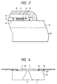
- Fig. 1A is a perspective view for explaining an ink-jet recording head of Example 1 of the present invention
- Fig. 1B is a sectional view taken along the plane 1B in Fig. 1A.
- Fig. 2 is a sectional view of the portion of the head taken along the plane 2 of Fig. 1A.
- Fig. 3A and Fig. 3B are views for explaining combination of a recording device substrate with a flexible film wiring substrate
- Fig. 3A is a perspective view showing a separated state
- Fig. 3B is a perspective view of a combined state.
- Fig. 4 is a sectional view taken along the line 4 - 4 in Fig. 3B.
- Fig. 5A and Fig. 5B are views for explaining connection of a flexible film wiring substrate with a recording device substrate in which electrodes are formed along the periphery of the recording device substrate, Fig. 5A is a perspective view showing a separated state, and Fig. 5B is a perspective view showing a combined state.
- Fig. 6A and Fig. 6B are views for explaining connection of a flexible film wiring substrate with a recording device substrate in which electrodes are formed in plural rows along the periphery of the recording device substrate, Fig. 6A is a perspective view showing a separated state, and Fig. 6B is a perspective view showing a combined state.
- Fig. 7 is a perspective view of an ink-jet recording head of Example 2 of the present invention.
- Fig. 8A is a sectional view taken along the plane 8A in Fig. 7
- Fig. 8B is a sectional view taken along the plane 8B in Fig. 7.
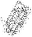
- Fig. 9 is an external perspective view of an example of an ink-jet recording apparatus (IJRA) equipped with a recording head of the present invention as the ink-jet head cartridge (IJC).
- IJRA ink-jet recording apparatus
- IJC ink-jet head cartridge
- Fig. 10 is a perspective view of a side shooter type recording head.
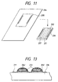
- Fig. 11 illustrates a concrete structure of a recording device substrate and a flexible film wiring substrate.
- Fig. 12A is a perspective view showing combination of a recording device substrate with a flexible film wiring substrate
- Fig. 12B is a sectional view taken along the line 12B - 12B in Fig. 12A.
- Fig. 13 is a sectional view taken along the plane 13 in Fig. 10.
- Fig. 1A is a perspective view of an ink-jet recording head of Example 1 of the present invention
- Fig. 1B is a sectional view taken along the plane 1B in Fig. 1A.
- Fig. 1A plural discharge openings 2 are formed for discharging ink at the central portion on the front face of a recording device substrate 1.
- an ink-supplying opening 3 (broken line in the drawing) is provided in a length nearly equal to the length of the row of the discharge openings.
- An ink supplying-holding member 18 holds three recording device substrates 1, and recording liquid is supplied to the respective recording device substrate 1.
- respective color recording liquids are separately held in respective color-recording device substrates 1 of the ink supplying-holding member 18.
- the ink supplying-holding member 18 holds single color recording liquid.
- electrodes on the recording device substrate 1 are electrically connected to electrode terminals on a flexible film wiring substrate 4.
- the input terminals of the flexible film wiring substrate are electrically connected to output terminals of a wiring substrate 6 having external input pads 5 for inputting electric signals of recording information and the like from a recording apparatus body to the ink-jet recording head.
- connection portions of the input terminals of respective flexible film wiring substrates 4 with the output terminals of the wiring substrate 6 are covered with a sealant 11 to prevent direct finger touch and ink attachment to the connection portion.
- the recording device substrates are held by the ink supplying-holding member 18 on a different face from the wiring substrate 6 on the ink supplying-holding member 18. With this constitution, the ink discharge direction (recording paper face) is different from the connection direction of the input pads 5 on the wiring substrate 6, thereby freedom in design of the paper feeding mechanism being increased.
- the output terminals 6' of the wiring substrate 6 and the input terminals 4' of the respective flexible film wiring substrates are connected electrically and fixed by hot pressing with an anisotropic conductive adhesion film composed of electroconductive particles 9' and an adhesive 9''.
- an anisotropic conductive adhesion film composed of electroconductive particles 9' and an adhesive 9''.
- the terminals (4', 6') are electrically connected by the electroconductive particles 9' and are fixed by the adhesive 9'', while the non-terminal portions are fixed by the adhesive 9'' without electrical connection.
- the aforementioned anisotropic conductive adhesion film 9, for example, may be composed mainly of electroconductive nickel particles of primary diameter of 2 to 6 ⁇ m and an epoxy resin.
- an anisotropic conductive adhesion film 9 the gold-plated output terminals 6' of the wiring substrate 6 and the gold-plated input terminals 4' of the respective flexible film wiring substrate are hot-pressed at a temperature of from 17°C to 250°C under a pressure of about 4 MPa. Thereby satisfactory electric connection and fixation can be achieved with a resistance of not higher than 10 m ⁇ for one terminal (terminal width: 170 ⁇ m).
- the anisotropic conductive adhesion film 9 as the connecting material renders unnecessary the use of a flux as the active material for removing an oxide film and dirt from the terminal portions, thus eliminating the adverse effects of splashing of the flux and ionic gas generation from the residue of the flux.
- the sealing agent 11 when the sealing agent 11 is mainly composed of the aforementioned epoxy resin, direct finger touch and attachment of splashed ink onto the terminal connection portions can be prevented by controlling the length of protrusion of the anisotropic conductive adhesive 9 from the end of the flexible film wiring substrate 4 to be not more than 0.5 mm.
- the anisotropic conductive film containing electroconductive particles is used for electric connection and fixation of the input terminals 4' of the flexible film wiring substrate 4 and the output terminals 6' of the wiring substrate 6.
- the electrical connection and fixation may be made by use of a thermosetting adhesive which contains no electroconductive particle by hot pressing.
- Figs. 3A and 3B illustrate structure of the connection between the recording device substrate 1 and the flexible film wiring substrate 4.
- Fig. 3A shows a separated state
- Fig. 3B shows the state of the recording device substrate fitted to the flexible film wiring substrate.
- Fig. 4 is a sectional view taken along the line 4 - 4 in Fig. 3B.
- a plurality of electrothermal converting elements are formed on the surface of the recording device substrate 1.
- Ink flow paths 19 are formed in the regions having the electrothermal converting elements.
- Plural discharge openings 2 are formed on the orifice face 7 constructing the ceiling of the ink paths 19 corresponding to the respective electrothermal converting elements.
- the ink paths 19 communicate to an ink supply opening 3 for supply of the recording liquid.
- the flexible film wiring substrate 4 has an aperture to uncover the orifice face 7 having the discharge openings 2 when the recording device substrate 1 is fitted thereto.
- electrode terminals 8 are provided to be connected to the electrodes 10 of the recording device substrate 1.
- the recording device substrate 1 is connected and fixed as shown in Fig. 4 by applying an epoxy type thermosetting adhesive 20 (or placing semi-cured thermosetting adhesive 20) on the portions of the electrodes 10 of the recording device substrate 1, or the electrode terminals 8 of the flexible film wiring substrate 4; positionally registering and temporarily bonding the electrodes 10 and the electrode terminals 8; and hot pressing with a heating jig from the side of the flexible film wiring substrate 4.
- the electrodes 10 and the electrode terminals 8 were connected electrically satisfactorily and fixed sufficiently under a pressure of 2 to 6 MPa at a resin-heating temperature of 160°C to 220°C for 2 to 10 seconds.
- the total of the thicknesses of the electrode 10, the electrode terminal 8, and the base film 8' is adjusted to be smaller than the height of the orifice face 7.
- the electrode 10 on the recording device substrate 1 has a thickness of 10 to 40 ⁇ m
- the electrode terminal 8 on the back face of the flexible film wiring substrate 4 has a thickness of 12 to 45 ⁇ m
- the base film 8' which is made of an organic resin and is a base of the flexible film wiring substrate has a thickness of 12 to 50 ⁇ m
- the orifice face 7 has a height of 20 to 50 ⁇ m.
- This constitution in which the total of the thicknesses of the electrode 10, the electrode terminal 8, and the base film 8' is smaller than the height of the orifice face 7 facilitates wiping with a rubber blade to remove ink drops and dirt such as paper powder adhering to the orifice face 7.
- connection portions (electrode portions) between the electrode 10 and the electrode terminal 8 are fixed and completely covered with the thermosetting adhesive 20. Thereby, direct finger touch with the electrode portion or ink attachment thereto is prevented. Thus, sealing of the electrode portions with a sealant is not necessary, and the sealing process is not required.
- the thermosetting adhesive 20 may be an anisotropic conductive adhesive containing electroconductive particles, and the electrodes 10 and the electrode terminals 8 may be electrically connected and fixed by the anisotropic conductive adhesive by hot pressing. In such connection and fixation by hot pressing with anisotropic conductive adhesive, the electrodes 10 and the electrode terminals 8 are electrically connected by the electroconductive particles and fixed by the adhesive, and in the portions where the terminal is not provided, the base film and the recording device substrate are bonded together by the adhesive without electric connection by electroconductive particles.
- the electrodes 10 and the electrode terminals 8 can be arranged as desired corresponding to the design.
- the electrodes 10 are formed along the periphery of the recording device substrate 4, and the electrode terminals 8 are formed around the aperture on the back face of the flexible film wiring substrate 4 corresponding to the positions of the electrodes 10.
- the recording device substrate 1 is bonded along the entire periphery to the flexible film wiring substrate 4 to improve the adhesion strength between the substrates without a vent formation, causing neither penetration nor attachment of the recording liquid through the vent hole.
- the electrodes 10 are formed in plural rows to increase the electrical connection density between the recording device substrate 1 and the flexible film wiring substrate 4.
- Such construction cannot readily be achieved in the structure shown in aforementioned Fig. 11 in which the electrode terminals 8 of the flexible film wiring substrate 4 protrude from the organic material substrate to the aperture.
- such a construction can be realized by providing the electrode terminals 8 on the reverse face of the flexible film wiring substrate 4 and connecting and fixing the electrode terminals to the electrode 10 of the recording device substrate 1 with an adhesive.
- the flexible film wiring substrate should be tightly held and protected in consideration of the connection with connector parts for external input pads for application of electric signals of recording information from the recording apparatus body to the ink-jet recording head.
- Fig. 7 is a perspective view of an ink-jet recording head of this Example 2 of the present invention.
- Fig. 8A is a sectional view taken along the plane 8A in Fig. 7
- Fig. 8B is a sectional view taken along the plane 8B in Fig. 7.
- the same reference numbers are used for the same members as in Fig. 1.
- the input terminal 4' of the flexible film wiring substrate 4 having the recording device substrates 1 fitted thereto is held between an output terminal 6' provided on the reverse face of the wiring substrate 6 having many external input pads 5 and an ink supplying-holding member 18.
- An anisotropic conductive adhesion film 9 is provided between the input terminal 4' of the flexible film wiring substrate 4 and the output terminal 6' of the wiring substrate 6 to connect electrically and fix the terminals (4' and 6') by hot pressing.
- the input terminals 4' of the flexible film wiring substrate 4 are held tightly and protected between the output terminals 6' on the reverse face of the wiring substrate 6 and the ink supplying-holding member 18. Thereby direct finger touch or ink attachment is prevented.
- connection portions of the input terminal of the flexible film wiring substrate 4 with the output terminal of the wiring substrate 6 are coated with a sealing agent 11 to prevent direct finger touch and ink penetration.
- the coating of the terminal connection portions with a sealing agent will prevent the penetration of ink and improve further the reliability of the terminal connection portions.
- the above Examples describe a side-shooter type recording head.
- the present invention also can be applied to an edge-shooter type of recording head, thereby obtaining the same effect as of the side-shootor type.
- the present invention also can be applied to a flexible film wiring substrate of a TCP (tape carrier package) having a recording device substrate fitted thereto by a TAB process to prevent deterioration of the printing quality.
- TCP tape carrier package
- the recording with the recording head of the present invention can be carried out on a recording medium such as paper, thread, fiber, cloth, leather, metal, plastics, glass, wood, ceramics or the like.
- the recording liquid for the recording head of the present invention is not limited to ink, and any material is useful which can be discharged and conduct recording on the above recording medium.
- Fig. 9 is an perspective external view of an example of an ink-jet recording apparatus (IJRA) employing an ink-jet recording head of the present invention as an ink-jet head cartridge (IJC).
- IJRA ink-jet recording apparatus
- IJC ink-jet head cartridge
- an ink-jet head cartridge (IJC) 120 has nozzles for discharging ink onto a recording face of a recording paper sheet fed onto a platen 124.
- a carriage HC 116 holds IJC 120, and is slidable along two parallel guide shafts 119A and 119B by a driving belt 118 driven by a motor 117. Thereby, the IJC 120 can reciprocate over the entire breadth of the recording paper sheet.
- a head recovery device 126 is placed at an end of the moving route of the IJC 120, for example, in opposition to the home position thereof.
- the head recovery device 126 is operated by the driving force applied through a transmission mechanism 123 to conduct capping of the IJC 120.
- a discharge recovery treatment is conducted such that the thickened ink is removed forcibly from the nozzle by sucking of the ink by a sucking means provided in the head recovery device 126 or by feeding of ink by a pressurizing means provided in the ink feeding path to the IJC 120.
- the IJC after the recording is protected by capping.
- a blade 130 made of a silicone rubber is placed as a wiping member at the side of the head recovery device 126.
- the blade 130 is held by a blade-holding member 130A in a cantilever state, and driven by the motor 122 and the transmission mechanism 123 similarly as the head recovery device 126 to fit to the discharging face of the IJC 120.
- the blade 130 is allowed to protrude to the movement route of the IJC 120 at a suitable time during the recording operation of IJC 120 or after the discharge recovery by the head recovery device 126 to wipe off condensed dew, wet, or dirt on the discharge face of the IJC 120.
- the above ink-jet recording apparatus is applicable to various apparatuses such as printers, copying machines, facsimile machines having a communication system, and word processors having a printer, and industrial recording apparatuses combined with other treatment apparatus.
- the present invention makes unnecessary the use of a flux to remove an oxide film or dirt, thereby preventing clogging of the discharge opening of the recording device substrate by a splashed flux; preventing attachment of ionic gas molecules evolved from residual flux after soldering to the vicinity of the discharge opening, which causes lowering of the water repellancy of the ink; or preventing attachment of the ionic gas molecules to the electrothermal converting element through the discharge opening, which causes lowering of the printing quality.
- an ink-jet recording head with high reliability can be provided.
- connection portions of electrode terminals of the flexible film wiring substrate with the electrodes of the recording device substrate need not be sealed with a sealant. Therefore, deterioration of printing quality owing to change in ink-wettability does not occur which may be caused by attachment of a volatile low molecular component or a solvent component to the orifice face, the nozzle inside walls, or the surface of the electrothermal converting elements. Thereby, printing can be conducted stably with high quality.
- the electrode portions coated with an adhesive are formed lower than the level of the orifice face having discharge openings. Therefore the interspace between the head and the recording medium can be determined by the distance between the orifice face and the recording medium, so that the head portion can be constituted more compactly. Further, the coated electrode portions are at a level lower than the orifice face, therefore, no trouble being caused in cleaning of the orifice face by a rubber blade.
- the electrode terminals of the flexible film wiring substrate and the electrodes of the recording device substrate are connected electrically and fixed by an anisotropic conductive adhesive containing electroconductive particles by hot pressing, a high temperature treatment at 350°C or a supersonic treatment is not required for the intermetallic bonding. Therefore, the nozzle member formed on the orifice face does not deteriorate, or the adhesion of the orifice face to the underlaying layer is not weakened, thereby the nozzle reliability being not impaired.
- the electrode terminals of the flexible film wiring substrate protrude from the organic base material, so that it is extremely difficult to form the electrode terminals in plural rows along the sides of the recording device substrate to increase the connection densities of the electrodes.
- the electrode terminals of the flexible film wiring substrate are provided on the reverse face thereof, whereby the electrodes of the recording device substrate can be formed in plural rows along the side of the substrate to increase the electrode connection density.
- an ink-jet recording head comprising at least one recording device substrate for discharging a recording liquid by pressure of bubble formation caused by thermal energy, a flexible film wiring substrate for fitting the recording device substrate thereto, an electrode pad for receiving control signals from outside for controlling thermal energy generation in the recording device substrate, and a wiring substrate connected electrically to the recording device substrate with interposition of the flexible film wiring substrate, wherein an input terminal of the flexible film wiring substrate and an output terminal of the wiring substrate are electrically connected to each other and fixed by a thermosetting adhesive by hot-pressing, and the connected electrode portion is coated with the thermosetting adhesive.
Landscapes
- Engineering & Computer Science (AREA)
- Manufacturing & Machinery (AREA)
- Particle Formation And Scattering Control In Inkjet Printers (AREA)
- Ink Jet (AREA)
Applications Claiming Priority (3)
| Application Number | Priority Date | Filing Date | Title |
|---|---|---|---|
| JP8202248A JPH1044418A (ja) | 1996-07-31 | 1996-07-31 | インクジェット記録ヘッドおよびそのヘッドを用いたインクジェット記録装置 |
| JP202248/96 | 1996-07-31 | ||
| JP20224896 | 1996-07-31 |
Publications (3)
| Publication Number | Publication Date |
|---|---|
| EP0822082A2 true EP0822082A2 (fr) | 1998-02-04 |
| EP0822082A3 EP0822082A3 (fr) | 1998-10-07 |
| EP0822082B1 EP0822082B1 (fr) | 2003-06-18 |
Family
ID=16454410
Family Applications (1)
| Application Number | Title | Priority Date | Filing Date |
|---|---|---|---|
| EP97113150A Expired - Lifetime EP0822082B1 (fr) | 1996-07-31 | 1997-07-30 | Tête d'enregistrement à jet d'encre, procédé de fabrication de la tête et appareil d'enregistrement à jet d'encre utilisant la tête |
Country Status (4)
| Country | Link |
|---|---|
| US (1) | US6241340B1 (fr) |
| EP (1) | EP0822082B1 (fr) |
| JP (1) | JPH1044418A (fr) |
| DE (1) | DE69722865T2 (fr) |
Cited By (3)
| Publication number | Priority date | Publication date | Assignee | Title |
|---|---|---|---|---|
| EP0916497A3 (fr) * | 1997-11-06 | 1999-12-22 | Seiko Epson Corporation | Tête d'enregistrement à jet d'encre |
| EP1232867A1 (fr) * | 2001-02-14 | 2002-08-21 | Hewlett-Packard Company | Circuit électrique pour ensemble de tête d'impression jet d'encre de grande dimension |
| EP1172217A3 (fr) * | 2000-07-10 | 2003-12-03 | Canon Kabushiki Kaisha | Tête d'enregistrement à jet d'encre et procédé de sa production |
Families Citing this family (37)
| Publication number | Priority date | Publication date | Assignee | Title |
|---|---|---|---|---|
| JP3592172B2 (ja) | 1999-01-27 | 2004-11-24 | キヤノン株式会社 | インクジェット記録ヘッドの製造方法、該製法によって製造されたインクジェット記録ヘッド及び該インクジェット記録ヘッドを搭載したインクジェット記録装置 |
| US7004652B2 (en) * | 2000-05-23 | 2006-02-28 | Silverbrook Research Pty Ltd | Printer for accommodating varying page thickness |
| ATE309102T1 (de) * | 2000-05-24 | 2005-11-15 | Silverbrook Res Pty Ltd | Sensor für die papierdicke in einem printer |
| JP3592208B2 (ja) * | 2000-07-10 | 2004-11-24 | キヤノン株式会社 | 液体噴射記録ヘッドおよびその製造方法 |
| JP3652321B2 (ja) | 2001-05-08 | 2005-05-25 | キヤノン株式会社 | インクジェット記録ヘッド |
| JP3603828B2 (ja) * | 2001-05-28 | 2004-12-22 | 富士ゼロックス株式会社 | インクジェット式記録ヘッド及びその製造方法並びにインクジェット式記録装置 |
| US6935726B2 (en) * | 2002-07-15 | 2005-08-30 | Canon Kabushiki Kaisha | Printing head and ink jet printing apparatus which performs printing with the printing head |
| US6834937B2 (en) | 2002-08-13 | 2004-12-28 | Lexmark International, Inc. | Printhead corrosion protection |
| US6951778B2 (en) * | 2002-10-31 | 2005-10-04 | Hewlett-Packard Development Company, L.P. | Edge-sealed substrates and methods for effecting the same |
| US6905342B2 (en) * | 2003-04-01 | 2005-06-14 | Hewlett-Packard Development Company, L.P. | Protected electrical interconnect assemblies |
| US7083267B2 (en) * | 2003-04-30 | 2006-08-01 | Hewlett-Packard Development Company, L.P. | Slotted substrates and methods and systems for forming same |
| US6913343B2 (en) * | 2003-04-30 | 2005-07-05 | Hewlett-Packard Development Company, L.P. | Methods for forming and protecting electrical interconnects and resultant assemblies |
| JP2005132102A (ja) * | 2003-10-09 | 2005-05-26 | Canon Inc | インクジェットヘッドおよび該ヘッドを備えるインクジェットプリント装置 |
| US7448734B2 (en) * | 2004-01-21 | 2008-11-11 | Silverbrook Research Pty Ltd | Inkjet printer cartridge with pagewidth printhead |
| US7118189B2 (en) * | 2004-05-28 | 2006-10-10 | Videojet Technologies Inc. | Autopurge printing system |
| JP2006012992A (ja) | 2004-06-23 | 2006-01-12 | Sharp Corp | 回路基板の電極接続構造 |
| KR100612325B1 (ko) * | 2004-07-16 | 2006-08-16 | 삼성전자주식회사 | 접착성 절연층을 갖는 잉크 카트리지, 그 제조 방법 및이를 장착한 화상 형성 장치 |
| WO2006009236A1 (fr) * | 2004-07-22 | 2006-01-26 | Canon Kabushiki Kaisha | Tête d’enregistrement à jet d’encre et appareil d’enregistrement à jet d’encre |
| US7425057B2 (en) | 2005-04-04 | 2008-09-16 | Canon Kabushiki Kaisha | Liquid discharge head and method for manufacturing the same |
| JP4687450B2 (ja) * | 2005-12-27 | 2011-05-25 | セイコーエプソン株式会社 | フレキシブル基板の実装方法、液滴吐出ヘッドの製造方法、液滴吐出ヘッド、及び液滴吐出装置 |
| US7794058B2 (en) * | 2006-05-29 | 2010-09-14 | Canon Kabushiki Kaisha | Liquid discharge head and method for manufacturing the same |
| US7810910B2 (en) * | 2006-06-29 | 2010-10-12 | Eastman Kodak Company | Fluid-ejecting device with simplified connectivity |
| JP5006680B2 (ja) | 2007-03-30 | 2012-08-22 | キヤノン株式会社 | インクジェット記録ヘッドおよびインクジェット記録ヘッドの製造方法 |
| JP2009226923A (ja) | 2008-02-26 | 2009-10-08 | Seiko Epson Corp | 液体噴射ヘッド及び液体噴射装置並びにアクチュエータ装置 |
| US8226212B2 (en) * | 2008-03-01 | 2012-07-24 | Hewlett-Packard Development Company, L.P. | Flexible circuit for fluid-jet precision-dispensing device cartridge assembly |
| JP5274356B2 (ja) * | 2009-04-23 | 2013-08-28 | キヤノン株式会社 | インクジェット記録ヘッド |
| US8628173B2 (en) * | 2010-06-07 | 2014-01-14 | Xerox Corporation | Electrical interconnect using embossed contacts on a flex circuit |
| US20120210580A1 (en) * | 2011-02-23 | 2012-08-23 | Dietl Steven J | Method of assembling an inkjet printhead |
| JP5372054B2 (ja) * | 2011-03-11 | 2013-12-18 | 東芝テック株式会社 | インクジェットヘッド |
| JP5358601B2 (ja) * | 2011-03-11 | 2013-12-04 | 東芝テック株式会社 | インクジェットヘッド |
| JP6907493B2 (ja) | 2016-09-28 | 2021-07-21 | ブラザー工業株式会社 | アクチュエータ装置、配線部材の接続構造、液体吐出装置、及び、アクチュエータ装置の製造方法 |
| JP6915250B2 (ja) | 2016-09-28 | 2021-08-04 | ブラザー工業株式会社 | アクチュエータ装置、液体吐出装置、及び、配線部材の接続構造 |
| JP7001373B2 (ja) * | 2017-06-15 | 2022-01-19 | キヤノン株式会社 | 液体吐出ヘッドとその製造方法 |
| JP7098350B2 (ja) * | 2018-02-28 | 2022-07-11 | キヤノン株式会社 | 接着シートを用いたインクジェット記録ヘッド及び製造方法 |
| JP2020179370A (ja) * | 2019-04-26 | 2020-11-05 | キヤノン株式会社 | 吐出材吐出装置、およびインプリント装置 |
| JP6806866B1 (ja) * | 2019-09-18 | 2021-01-06 | キヤノン株式会社 | 液体吐出用ヘッドとその製造方法、並びに液体吐出装置 |
| JP7730674B2 (ja) * | 2021-06-25 | 2025-08-28 | キヤノン株式会社 | 液体吐出ヘッド |
Family Cites Families (10)
| Publication number | Priority date | Publication date | Assignee | Title |
|---|---|---|---|---|
| JPS5989164A (ja) * | 1982-11-10 | 1984-05-23 | Seiko Epson Corp | マルチノズルインクジエツトヘツドユニツト |
| JP3094489B2 (ja) * | 1991-04-05 | 2000-10-03 | セイコーエプソン株式会社 | インクジェットプリントヘッドとそれを用いたインクジェットプリント装置、及びインクジェットプリントヘッドの製造方法 |
| JPH04345858A (ja) * | 1991-05-23 | 1992-12-01 | Seiko Epson Corp | インクジェットヘッド |
| JPH05196952A (ja) * | 1991-10-02 | 1993-08-06 | Canon Inc | 電気的接続構造及び電気的接続方法 |
| JPH05166998A (ja) | 1991-12-12 | 1993-07-02 | Dainippon Printing Co Ltd | リードフレームにおけるフレキシブル配線基板とプリント回路基板との接続方法およびその接続方法に用いられるフレキシブル配線基板部材 |
| US5459500A (en) * | 1992-03-25 | 1995-10-17 | Scitex Digital Printing, Inc. | Charge plate connectors and method of making |
| US5537133A (en) | 1992-04-02 | 1996-07-16 | Hewlett-Packard Company | Restraining element for a print cartridge body to reduce thermally induced stress |
| US5442386A (en) | 1992-10-13 | 1995-08-15 | Hewlett-Packard Company | Structure and method for preventing ink shorting of conductors connected to printhead |
| US5422667A (en) * | 1992-12-02 | 1995-06-06 | General Ribbon Corporation | Ink jet printing cartridge with circuit element protection system |
| EP0644051A1 (fr) * | 1993-09-16 | 1995-03-22 | Hewlett-Packard Company | Un ciruit intermédiaire flexible pour une cartouche d'impression à jet d'encre ayant orifices plusieurs |
-
1996
- 1996-07-31 JP JP8202248A patent/JPH1044418A/ja active Pending
-
1997
- 1997-07-29 US US08/902,324 patent/US6241340B1/en not_active Expired - Lifetime
- 1997-07-30 DE DE69722865T patent/DE69722865T2/de not_active Expired - Lifetime
- 1997-07-30 EP EP97113150A patent/EP0822082B1/fr not_active Expired - Lifetime
Cited By (8)
| Publication number | Priority date | Publication date | Assignee | Title |
|---|---|---|---|---|
| EP0916497A3 (fr) * | 1997-11-06 | 1999-12-22 | Seiko Epson Corporation | Tête d'enregistrement à jet d'encre |
| US6190006B1 (en) | 1997-11-06 | 2001-02-20 | Seiko Epson Corporation | Ink-jet recording head |
| EP1172217A3 (fr) * | 2000-07-10 | 2003-12-03 | Canon Kabushiki Kaisha | Tête d'enregistrement à jet d'encre et procédé de sa production |
| US6659591B2 (en) | 2000-07-10 | 2003-12-09 | Canon Kabushiki Kaisha | Ink jet recording head and producing method for the same |
| EP1741558A3 (fr) * | 2000-07-10 | 2007-01-17 | Canon Kabushiki Kaisha | Procédé de production d'une tête d'enregistrement à jet d'encre |
| EP1232867A1 (fr) * | 2001-02-14 | 2002-08-21 | Hewlett-Packard Company | Circuit électrique pour ensemble de tête d'impression jet d'encre de grande dimension |
| US6557976B2 (en) | 2001-02-14 | 2003-05-06 | Hewlett-Packard Development Company, L.P. | Electrical circuit for wide-array inkjet printhead assembly |
| US6843552B2 (en) | 2001-02-14 | 2005-01-18 | Hewlett-Packard Development Company, L.P. | Electrical circuit for printhead assembly |
Also Published As
| Publication number | Publication date |
|---|---|
| DE69722865T2 (de) | 2004-05-13 |
| EP0822082B1 (fr) | 2003-06-18 |
| US6241340B1 (en) | 2001-06-05 |
| DE69722865D1 (de) | 2003-07-24 |
| EP0822082A3 (fr) | 1998-10-07 |
| JPH1044418A (ja) | 1998-02-17 |
Similar Documents
| Publication | Publication Date | Title |
|---|---|---|
| US6241340B1 (en) | Ink-jet recording head, process for producing the head and ink-jet recording apparatus employing the head | |
| US6609782B2 (en) | Liquid jet recording head and method of manufacturing the same | |
| US6659591B2 (en) | Ink jet recording head and producing method for the same | |
| US6186616B1 (en) | Ink jet head having an improved orifice plate, a method for manufacturing such ink jet heads, and an ink jet apparatus provided with such ink jet head | |
| EP0539993B1 (fr) | Tête d'impression à jet d'encre et son procédé de fabrication | |
| CN101456284B (zh) | 液体喷出头 | |
| EP1362703B1 (fr) | Tête d'enregistrement à jet d'encre et son procédé de fabrication | |
| US20110018930A1 (en) | Feed slot protective coating | |
| US7025439B2 (en) | Ink jet printer with extended nozzle plate and method | |
| JP3679740B2 (ja) | インクジェット記録ヘッドおよびインクジェット記録装置 | |
| JP2000108344A (ja) | インクジェット記録装置 | |
| JP4334751B2 (ja) | インクジェットヘッド及びインクジェット記録装置 | |
| JPH11147314A (ja) | インクジェット記録ヘッド及びインクジェット記録装置 | |
| JP4145481B2 (ja) | インクジェットヘッドの製造方法、インクジェットヘッド、インクジェット記録装置及び画像形成装置 | |
| JP3656800B2 (ja) | インクジェット記録装置及びその製造方法 | |
| EP0829359A2 (fr) | Tête d'enregistrement à jet d'encre et dispositif d'enregistrement à jet d'encre comportant une telle tête | |
| JP2003237073A (ja) | 液体吐出ヘッド、液体吐出ヘッドの製造方法、および液体吐出記録装置 | |
| JP2000071448A (ja) | インクジェット記録装置 | |
| JP2002103632A (ja) | 液滴吐出ヘッド及びその製造方法並びにインクジェット記録装置 | |
| JP4080152B2 (ja) | インクジェットヘッドの製造方法、インクジェットヘッド及びインクジェット記録装置 | |
| JP2007055184A (ja) | インクジェット記録ヘッド | |
| JP2006026950A (ja) | 液体吐出ヘッドおよび画像形成装置 | |
| JPH0948126A (ja) | 液体噴射記録ヘッドおよびその製造方法ならびに前記液体噴射記録ヘッドを搭載する液体噴射記録装置 | |
| JP2001232794A (ja) | インクジェットヘッド、その製造方法、インクジェット記録装置、及び、アクチュエータ | |
| JP2002254638A (ja) | インクジェットヘッド及びインクジェット記録装置 |
Legal Events
| Date | Code | Title | Description |
|---|---|---|---|
| PUAI | Public reference made under article 153(3) epc to a published international application that has entered the european phase |
Free format text: ORIGINAL CODE: 0009012 |
|
| AK | Designated contracting states |
Kind code of ref document: A2 Designated state(s): DE FR GB IT |
|
| AX | Request for extension of the european patent |
Free format text: AL;LT;LV;RO;SI |
|
| PUAL | Search report despatched |
Free format text: ORIGINAL CODE: 0009013 |
|
| AK | Designated contracting states |
Kind code of ref document: A3 Designated state(s): AT BE CH DE DK ES FI FR GB GR IE IT LI LU MC NL PT SE |
|
| 17P | Request for examination filed |
Effective date: 19990222 |
|
| AKX | Designation fees paid |
Free format text: DE FR GB IT |
|
| 17Q | First examination report despatched |
Effective date: 20010529 |
|
| GRAG | Despatch of communication of intention to grant |
Free format text: ORIGINAL CODE: EPIDOS AGRA |
|
| GRAG | Despatch of communication of intention to grant |
Free format text: ORIGINAL CODE: EPIDOS AGRA |
|
| GRAH | Despatch of communication of intention to grant a patent |
Free format text: ORIGINAL CODE: EPIDOS IGRA |
|
| GRAH | Despatch of communication of intention to grant a patent |
Free format text: ORIGINAL CODE: EPIDOS IGRA |
|
| GRAA | (expected) grant |
Free format text: ORIGINAL CODE: 0009210 |
|
| AK | Designated contracting states |
Designated state(s): DE FR GB IT |
|
| REG | Reference to a national code |
Ref country code: GB Ref legal event code: FG4D |
|
| REF | Corresponds to: |
Ref document number: 69722865 Country of ref document: DE Date of ref document: 20030724 Kind code of ref document: P |
|
| ET | Fr: translation filed | ||
| PLBE | No opposition filed within time limit |
Free format text: ORIGINAL CODE: 0009261 |
|
| STAA | Information on the status of an ep patent application or granted ep patent |
Free format text: STATUS: NO OPPOSITION FILED WITHIN TIME LIMIT |
|
| 26N | No opposition filed |
Effective date: 20040319 |
|
| REG | Reference to a national code |
Ref country code: FR Ref legal event code: PLFP Year of fee payment: 19 |
|
| PGFP | Annual fee paid to national office [announced via postgrant information from national office to epo] |
Ref country code: GB Payment date: 20150727 Year of fee payment: 19 Ref country code: DE Payment date: 20150731 Year of fee payment: 19 |
|
| PGFP | Annual fee paid to national office [announced via postgrant information from national office to epo] |
Ref country code: FR Payment date: 20150729 Year of fee payment: 19 |
|
| PGFP | Annual fee paid to national office [announced via postgrant information from national office to epo] |
Ref country code: IT Payment date: 20150708 Year of fee payment: 19 |
|
| REG | Reference to a national code |
Ref country code: DE Ref legal event code: R119 Ref document number: 69722865 Country of ref document: DE |
|
| GBPC | Gb: european patent ceased through non-payment of renewal fee |
Effective date: 20160730 |
|
| PG25 | Lapsed in a contracting state [announced via postgrant information from national office to epo] |
Ref country code: DE Free format text: LAPSE BECAUSE OF NON-PAYMENT OF DUE FEES Effective date: 20170201 Ref country code: FR Free format text: LAPSE BECAUSE OF NON-PAYMENT OF DUE FEES Effective date: 20160801 |
|
| REG | Reference to a national code |
Ref country code: FR Ref legal event code: ST Effective date: 20170331 |
|
| PG25 | Lapsed in a contracting state [announced via postgrant information from national office to epo] |
Ref country code: GB Free format text: LAPSE BECAUSE OF NON-PAYMENT OF DUE FEES Effective date: 20160730 |
|
| PG25 | Lapsed in a contracting state [announced via postgrant information from national office to epo] |
Ref country code: IT Free format text: LAPSE BECAUSE OF NON-PAYMENT OF DUE FEES Effective date: 20160730 |