EP0824239A2 - Sekundärkanal für ein Fibre-Channel-Systemschnittstellenbus - Google Patents
Sekundärkanal für ein Fibre-Channel-Systemschnittstellenbus Download PDFInfo
- Publication number
- EP0824239A2 EP0824239A2 EP97305893A EP97305893A EP0824239A2 EP 0824239 A2 EP0824239 A2 EP 0824239A2 EP 97305893 A EP97305893 A EP 97305893A EP 97305893 A EP97305893 A EP 97305893A EP 0824239 A2 EP0824239 A2 EP 0824239A2
- Authority
- EP
- European Patent Office
- Prior art keywords
- bus
- circuit
- point
- memory
- information
- Prior art date
- Legal status (The legal status is an assumption and is not a legal conclusion. Google has not performed a legal analysis and makes no representation as to the accuracy of the status listed.)
- Withdrawn
Links
Images


Classifications
-
- G—PHYSICS
- G06—COMPUTING OR CALCULATING; COUNTING
- G06F—ELECTRIC DIGITAL DATA PROCESSING
- G06F13/00—Interconnection of, or transfer of information or other signals between, memories, input/output devices or central processing units
- G06F13/38—Information transfer, e.g. on bus
- G06F13/42—Bus transfer protocol, e.g. handshake; Synchronisation
- G06F13/4265—Bus transfer protocol, e.g. handshake; Synchronisation on a point to point bus
- G06F13/4278—Bus transfer protocol, e.g. handshake; Synchronisation on a point to point bus using an embedded synchronisation
Definitions
- the present invention relates to a secondary channel connected to a point-to-point bus.
- the secondary channel is adapted to extract selected information from the point-to-point bus and provide the selected information to other circuits besides the point-to-point circuitry. More specifically, the present invention relates to the extraction of selected information from a Tachyon system interface bus and provide the selected information to a secondary circuit.
- Fibre channels were created to provide a practical, inexpensive and expandable means for quickly transferring data between workstations, mainframes, super computers, desktop computers, storage devices, network servers and other peripherals.
- Fibre channel is the general name of an integrated set of standards developed by the American National Standards Institute (ANSI).
- a channel provides a direct or switched point-to-point connection between communication devices.
- a channel is typically hardware-intensive and transports data at high speed with low overhead.
- a network is an aggregation of distributed nodes (like workstations, file servers or peripherals) with its own protocol that supports interaction among these nodes.
- a network has relatively high overhead since it is software-intensive and consequently slower than a channel.
- Tachyon which interfaces with a fibre channel and operates as a controller.
- the Tachyon controller receives and transmits over a fibre channel.
- the Tachyon controller also provides a Tachyon system interface bus (TSI bus) for interfacing the Tachyon controller with high speed devices that can handle bursts of data.
- TSI bus is basically a high speed point-to-point interconnect bus. It can be connected directly to a minicomputer or converted, via a bridge circuit, to other types of bus protocols such as that on a PCI bus.
- data may be designated to be stored in a storage device via a SCSI controller.
- a local microprocessor may have to interpret the data stream present on the PCI bus and schedule a data transfer into a memory device such as a disk drive. After the data transfer is scheduled by the local microprocessor, then the SCSI controller will proceed to transfer data which originated from the fibre channel into a memory storage device.
- a local microprocessor must read and interpret control commands that are present in the data and determine what should be done with the data that is now present on the PCI bus.
- control commands it would be useful for the control commands to be ex tracted from the TSI data stream at a time before the data is reformatted on to a PCI bus. This would enable the mi croprocessor to schedule a data transfer into, for example, a SCSI controller, at the same time the data stream is ready and available on the PCI bus.
- the present invention relates to providing a secondary channel, connected to a point-to-point burst style bus, that is adapted to extract or provided predetermined information, such as control information, from or to the burst style bus. That is, the secondary channel shares a point-to-point bus with the two point-to-point devices.
- the present invention relates to a secondary channel for a point-to-point burst style bus associated with a computer system.
- the point-to-point bus may originate as a standardized bus from a fibre channel controller.
- the point-to-point bus connects to another circuit which may be a bridge circuit, a minicomputer or a peripheral device.
- a secondary channel is also connected to the point-to-point bus and is adapted to share the bus by receiving information having predetermined addresses.
- the information recieved by the secondary channel can be stored in a memory that is shared with a processor.
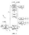
- the exemplary embodiment of the present secondary channel for a fibre channel interface controller system interface bus 10 preferably requires a fibre channel controller 12 such as a Tachyon controller.
- a fibre channel controller 12 such as a Tachyon controller.
- Other fibre channel controllers could be used without departing from the sprit of the present invention.
- the Tachyon controller 12 is adapted to receive and transmit information via a fibre channel 14.
- the Tachyon controller 12 converts the fibre channel information to a standardized bus protocol referred to as a TSI bus 16.
- the preferred Tachyon controller 12 is manufactured by Hewlett Packard and the specification therefore is hereby incorporated by reference.
- the TSI bus 16 is preferably converted by a "bridge circuit" 18 to a standardized bus protocol for a PCI bus 20. Furthermore, a secondary channel bus 22 is connected to the TSI bus 16. The data on the TSI bus 16 is being clocked at preferably 33 MHZ.
- the TSI bus 16 is a high speed data burst bus which cannot be slowed down or sped up.
- the TSI bus 16 was designed to be a point-to-point bus so that data can be sent from the fibre channel controller 12 to another device at a high data rate.
- the fibre channel controller 12 passes at least two types of information onto the TSI bus 16: 1) data, which may have to be stored on a disk 23; and 2) control information which defines, for example, what is to be done with the data.
- the secondary channel bus 22 is connected to a secondary channel bus arbitrator 24.
- the secondary channel bus arbitrator 24 is connected via a bus to a memory circuit 26.
- the memory circuit 26 is preferably SRAM that can operate at a minimum clock rate of 66 MHz. Other memory circuitry could be utilized in the present invention, but the memory must be able to be clocked at a minimum of 66 MHz.
- a local processor 28 is connected to the memory 26.
- the PCI bus 20 is connected to the local processor and to other peripheral devices such at SCSI controllers 29 and cache memories.
- the operation of the preferred embodiment of the present secondary channel for a fibre channel controller system interface bus 10 is straight forward.
- the goal of the exemplary embodiment is increase the speed at which data can be retrieved or provided to a fibre interface.
- the present invention is designed to bypass the intermediate transfer stage (the bridge circuit 18) of control information and thereby increase the speed that data can be directed to a designated device (such as a disk 23).
- FIGURE 2 depicts a flow chart indicating how the exemplary secondary channel 10 operates.
- the local processor 28 is requesting to read or write to the memory 26. If the local processor 28 is requesting to read or write to or from the memory 26, the secondary channel bus arbitrator 24 requires that the bridge circuit 18 does not have a grant (control) of the TSI bus 16 S2. The local processor 28 will provide an address and information to the secondary channel bus arbitrator 24 and the secondary channel bus arbitrator 24 will clock the information into the memory 26 S3.
- the fibre channel controller 12 takes control of the TSI bus 16 S4.
- the fibre channel controller 12 provides addresses and information to the TSI bus 16 S5.
- the fibre channel controller 12 on a first cycle, places an ADDRESS VALID CHIP SELECT signal and an ADDRESS on the TSI bus 16. These signals are clocked into the bridge circuit 18 and stored in latches (not shown) so the address can be sent at a later time to the memory if necessary.
- the bridge circuit 18 determines if the ADDRESS is an address for the memory 26 or an address for the bridge circuit 18. If the ADDRESS is for the memory 26 then the bridge circuit 18 places a VALID MEM_CYCLE signal on the TSI bus 16 indicating that the information following the address is to be stored in the memory 26 S6. The secondary channel arbitrator 24 notices the VALID MEM_CYCLE on the TSI bus 16 and allows information following the address to be sent directly to the memory 26 S8. If there is not a VALID MEM_CYCLE signal provided by the bridge circuit 18 then the information following the address is sent through the bridge circuit 18 and transformed to the PCI protocol S8. In the preferred embodiment of the present invention control information is sent directly from the TSI bus 16 to the memory 26 and data information is transformed, via the bridge circuit 18, to the PCI protocol and then clocked onto the PCI bus 20.
- the address and control information could both be transformed to a PCI protocol via the bridge circuit 18 and then placed on the PCI bus 20. Once on the PCI bus 20 the information could be placed in the memory 26 or provided to the local processor 28 or other devices on the PCI bus.
- the process of transforming the address and information to a PCI protocol takes additional clock cycles not required in the present invention.
- the present invention provides control information to the local processor 28 via the memory more quickly because the control information is extracted from the TSI bus prior to any transformation to the PCI protocol.
- the local processor 28 can determine where information related to the control signal (usually data following the control signal) should go more quickly because the control information is available to the local processor 28 quite a few cycles before the data coming from the TSI bus 16 is being transformed by the bridge circuit 18 and placed on the PCI bus 20.
- the present exemplary embodiment requires the fibre channel controller 12 to be set up to provide and control a TSI bus 16, the bridge circuit 18 to be connected to the TSI bus 16 and set up to determine if the information on the TSI bus is to go to the PCI bus 20 or to the memory 26, and the secondary channel arbitrator 24 be set up to receive information having addresses designating the information to go to memory 28.
- the exemplary embodiment of the present invention may include a local processor 28 that can read and write information from and to the memory 26 without interfering with the TSI bus 16 and information coming from the TSI bus 16 designated for memory.
- the memory 26 is, in essence, shared between the TSI bus 16 and the local processor 28. Furthermore, the memory 26 is clocked preferably at a speed which is twice as fast at the clock rate of the TSI bus 16. For example, if the TSI bus 16 is operating at a clock rate of 33 MHz, then the memory 26 is being clocked synchronously at 66 MHz. As long at the memory 26 is clocked at a speed which is a multiple of the clock speed of the TSI bus, then there can be time (at least a half a 33 MHz clock cycle) to decode an address on the TSI bus 16 and determine whether information following the address is to go to the memory 26 or to the bridge circuit 18 and onto the PCI bus 20.
- the present invention allows a point-to point bus, such as a TSI bus, to be shared. Without the present invention, all information coming from the fibre channel controller 12 would have to go to the TSI bus 16 and then to the bridge circuit 18 where it would be converted to another protocol such as PCI.
- the present invention allows a point-to-point bus to be more than a point-to-point bus.
- the advantage is that predetermined types of information, such as control signals, can be extracted from the point-to-point bus and used by other circuitry while other information, such as data, can continue on the TSI bus 16 and thereby be acted on more quickly by other circuitry, such as a local processor, because the other circuitry has already received the control signals associated with the data.
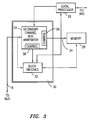
- FIGURE 3 depicts a block diagram of a portion of the present invention.
- the TSI bus 16 is connected to the secondary channel circuitry 30.
- the secondary channel cir cuitry 30, in this embodiment, has two basic blocks: 1) the secondary bus arbitrator 24; and 2) quick switches 32.
- the secondary channel bus arbitrator 24 receives control signals from the bridge circuit (not shown) via the TSI bus 16. In response to the control signals from the bridge circuit, the secondary channel bus arbitrator 24 instructs the quick switches 32 to switch the TSI bus 16 so that: a) the TSI bus can provide or be provided information to or from the memory; or b) the local processor can provide or be provided information to or from the memory.
- the bridge circuit de termines were an address, received from the TSI bus 16, is to go. If the address is for the memory, the bridge circuit provides a signal, via the TSI bus 16, to the secondary channel circuitry 30. Within the secondary channel circuitry 30, the memory is addressed via the control lines 34 while the information to be sent to memory 26 is switched via the quick switches 32 and send to the memory 26 for storage.
- the TSI bus 16 is clocked at approximately 33 MHz. In order to be able to decode the address on the TSI bus 16 and control the memory 26 fast enough to handle a burst of data from the TSI bus 16 (i.e.
- the control circuitry for the quick switches 38 and the memory 36 must be clocked synchronously at two times the frequency of the TSI bus clock which is approximately 66 MHz. This will allow one full clock cycle for each half TSI clock cycle.
- the address is decoded and during the second half of the clock cycle the secondary channel circuitry 30 can operate to have data read or written into or out of the memory.
- the local processor 28 can address the memory 26 and read or write information.
- FIGURE 4 depicts a block diagram of an exemplary sec ondary channel bus arbitrator 24.
- the secondary bus arbi trator 24 receives selected signals from the TSI bus 16. These signals are decoded in a decode circuit.
- the decode circuit 40 also receives signals from the local processor 28. In essence the decode circuit determines whether the TSI bus 16 or the local processor 28 or neither are requesting to read or write the memory 26. Based on the determination of the decode circuit 40, the control logic for the quick switches 42 and the control logic for the memory 44 are triggered to either allow the TSI bus 16 to read or write the memory 26, or to allow the local processor 28 to read or write the memory 26.
- the present invention is a significant improvement in the art because it enables selected control information to be received by a memory circuit and read by a local processor in a more timely manner. Also, a memory circuit is shared by a bursting point-to-point bus and a local processor. Furthermore, selected control information may bypass the intermediate transfer and reformatting of the bridge circuit.
- the present invention is believed to be especially effective when configured and employed as described herein, however, those skilled in the art will readily recognize that numerous variations and substitutions may be made in the invention and its use and configuration to achieve substantially the same results as achieved by the embodiments expressly described herein. Each of the variations is intended to be included in the description herein and forms a part of the present invention.
Landscapes
- Engineering & Computer Science (AREA)
- Theoretical Computer Science (AREA)
- Physics & Mathematics (AREA)
- General Engineering & Computer Science (AREA)
- General Physics & Mathematics (AREA)
- Bus Control (AREA)
Applications Claiming Priority (2)
| Application Number | Priority Date | Filing Date | Title |
|---|---|---|---|
| US692516 | 1985-01-18 | ||
| US08/692,516 US5848251A (en) | 1996-08-06 | 1996-08-06 | Secondary channel for command information for fibre channel system interface bus |
Publications (2)
| Publication Number | Publication Date |
|---|---|
| EP0824239A2 true EP0824239A2 (de) | 1998-02-18 |
| EP0824239A3 EP0824239A3 (de) | 1999-07-28 |
Family
ID=24780896
Family Applications (1)
| Application Number | Title | Priority Date | Filing Date |
|---|---|---|---|
| EP97305893A Withdrawn EP0824239A3 (de) | 1996-08-06 | 1997-08-04 | Sekundärkanal für ein Fibre-Channel-Systemschnittstellenbus |
Country Status (3)
| Country | Link |
|---|---|
| US (1) | US5848251A (de) |
| EP (1) | EP0824239A3 (de) |
| JP (1) | JPH10149330A (de) |
Families Citing this family (33)
| Publication number | Priority date | Publication date | Assignee | Title |
|---|---|---|---|---|
| US5751715A (en) * | 1996-08-08 | 1998-05-12 | Gadzoox Microsystems, Inc. | Accelerator fiber channel hub and protocol |
| US5978379A (en) * | 1997-01-23 | 1999-11-02 | Gadzoox Networks, Inc. | Fiber channel learning bridge, learning half bridge, and protocol |
| US6000020A (en) * | 1997-04-01 | 1999-12-07 | Gadzoox Networks, Inc. | Hierarchical storage management from a mirrored file system on a storage network segmented by a bridge |
| JP3228182B2 (ja) * | 1997-05-29 | 2001-11-12 | 株式会社日立製作所 | 記憶システム及び記憶システムへのアクセス方法 |
| US5970070A (en) * | 1997-08-20 | 1999-10-19 | Sun Microsystems, Inc. | Communication controllers and methods therefor |
| USRE42761E1 (en) | 1997-12-31 | 2011-09-27 | Crossroads Systems, Inc. | Storage router and method for providing virtual local storage |
| US5941972A (en) | 1997-12-31 | 1999-08-24 | Crossroads Systems, Inc. | Storage router and method for providing virtual local storage |
| US6209023B1 (en) * | 1998-04-24 | 2001-03-27 | Compaq Computer Corporation | Supporting a SCSI device on a non-SCSI transport medium of a network |
| US7430171B2 (en) * | 1998-11-19 | 2008-09-30 | Broadcom Corporation | Fibre channel arbitrated loop bufferless switch circuitry to increase bandwidth without significant increase in cost |
| US8225002B2 (en) | 1999-01-22 | 2012-07-17 | Network Disk, Inc. | Data storage and data sharing in a network of heterogeneous computers |
| US6549988B1 (en) | 1999-01-22 | 2003-04-15 | Ilya Gertner | Data storage system comprising a network of PCs and method using same |
| JP4091195B2 (ja) * | 1999-02-08 | 2008-05-28 | 富士通株式会社 | インタフェース制御装置及びインタフェース制御方法 |
| JP2001167040A (ja) * | 1999-12-14 | 2001-06-22 | Hitachi Ltd | 記憶サブシステム及び記憶制御装置 |
| US6671727B1 (en) | 1999-12-20 | 2003-12-30 | Lsi Logic Corporation | Methodology for providing persistent target identification in a fibre channel environment |
| US7657727B2 (en) * | 2000-01-14 | 2010-02-02 | Hitachi, Ltd. | Security for logical unit in storage subsystem |
| US6684209B1 (en) * | 2000-01-14 | 2004-01-27 | Hitachi, Ltd. | Security method and system for storage subsystem |
| JP4651230B2 (ja) * | 2001-07-13 | 2011-03-16 | 株式会社日立製作所 | 記憶システム及び論理ユニットへのアクセス制御方法 |
| US6629156B1 (en) * | 2000-03-02 | 2003-09-30 | Lsi Logic Corporation | Fibre Channel service parameter cache |
| JP4719957B2 (ja) * | 2000-05-24 | 2011-07-06 | 株式会社日立製作所 | 記憶制御装置及び記憶システム並びに記憶システムのセキュリティ設定方法 |
| US6981070B1 (en) * | 2000-07-12 | 2005-12-27 | Shun Hang Luk | Network storage device having solid-state non-volatile memory |
| US6804819B1 (en) | 2000-09-18 | 2004-10-12 | Hewlett-Packard Development Company, L.P. | Method, system, and computer program product for a data propagation platform and applications of same |
| US6977927B1 (en) | 2000-09-18 | 2005-12-20 | Hewlett-Packard Development Company, L.P. | Method and system of allocating storage resources in a storage area network |
| US7386610B1 (en) | 2000-09-18 | 2008-06-10 | Hewlett-Packard Development Company, L.P. | Internet protocol data mirroring |
| US6862648B2 (en) * | 2000-10-30 | 2005-03-01 | Sun Microsystems, Inc. | Interface emulation for storage devices |
| US6606690B2 (en) | 2001-02-20 | 2003-08-12 | Hewlett-Packard Development Company, L.P. | System and method for accessing a storage area network as network attached storage |
| US7239636B2 (en) | 2001-07-23 | 2007-07-03 | Broadcom Corporation | Multiple virtual channels for use in network devices |
| US7295555B2 (en) | 2002-03-08 | 2007-11-13 | Broadcom Corporation | System and method for identifying upper layer protocol message boundaries |
| US7934021B2 (en) | 2002-08-29 | 2011-04-26 | Broadcom Corporation | System and method for network interfacing |
| US7346701B2 (en) | 2002-08-30 | 2008-03-18 | Broadcom Corporation | System and method for TCP offload |
| US7313623B2 (en) | 2002-08-30 | 2007-12-25 | Broadcom Corporation | System and method for TCP/IP offload independent of bandwidth delay product |
| EP1554842A4 (de) | 2002-08-30 | 2010-01-27 | Corporation Broadcom | System und verfahren zum behandeln von ausserhalb der reihenfolge auftretenden rahmen |
| US8180928B2 (en) | 2002-08-30 | 2012-05-15 | Broadcom Corporation | Method and system for supporting read operations with CRC for iSCSI and iSCSI chimney |
| US9465763B2 (en) | 2013-06-17 | 2016-10-11 | Altera Corporation | Bridge circuitry for communications with dynamically reconfigurable circuits |
Family Cites Families (6)
| Publication number | Priority date | Publication date | Assignee | Title |
|---|---|---|---|---|
| WO1993004432A2 (en) * | 1991-08-16 | 1993-03-04 | Multichip Technology | High-performance dynamic memory system |
| US5412782A (en) * | 1992-07-02 | 1995-05-02 | 3Com Corporation | Programmed I/O ethernet adapter with early interrupts for accelerating data transfer |
| US5471586A (en) * | 1992-09-22 | 1995-11-28 | Unisys Corporation | Interface system having plurality of channels and associated independent controllers for transferring data between shared buffer and peripheral devices independently |
| US5590286A (en) * | 1993-10-07 | 1996-12-31 | Sun Microsystems, Inc. | Method and apparatus for the pipelining of data during direct memory accesses |
| US5574945A (en) * | 1993-11-04 | 1996-11-12 | International Business Machines Corporation | Multi channel inter-processor coupling facility processing received commands stored in memory absent status error of channels |
| US5611056A (en) * | 1994-08-31 | 1997-03-11 | Unisys Corporation | Method for controlling the expansion of connections to a SCSI bus |
-
1996
- 1996-08-06 US US08/692,516 patent/US5848251A/en not_active Expired - Fee Related
-
1997
- 1997-08-04 EP EP97305893A patent/EP0824239A3/de not_active Withdrawn
- 1997-08-06 JP JP9212197A patent/JPH10149330A/ja active Pending
Also Published As
| Publication number | Publication date |
|---|---|
| EP0824239A3 (de) | 1999-07-28 |
| JPH10149330A (ja) | 1998-06-02 |
| US5848251A (en) | 1998-12-08 |
Similar Documents
| Publication | Publication Date | Title |
|---|---|---|
| US5848251A (en) | Secondary channel for command information for fibre channel system interface bus | |
| US6757768B1 (en) | Apparatus and technique for maintaining order among requests issued over an external bus of an intermediate network node | |
| US6223238B1 (en) | Method of peer-to-peer mastering over a computer bus | |
| US5594882A (en) | PCI split transactions utilizing dual address cycle | |
| US5761462A (en) | Method and system for supporting peripheral component interconnect (PCI) peer-to-peer access across multiple PCI host bridges within a data-processing system | |
| JP4083987B2 (ja) | 多重レベル接続識別を備えた通信システム | |
| US5925120A (en) | Self-contained high speed repeater/lun converter which controls all SCSI operations between the host SCSI bus and local SCSI bus | |
| US20020168966A1 (en) | I/O unit emulation | |
| US7016994B2 (en) | Retry mechanism for blocking interfaces | |
| US6889266B1 (en) | Method for delivering packet boundary or other metadata to and from a device using direct memory controller | |
| US6301632B1 (en) | Direct memory access system and method to bridge PCI bus protocols and hitachi SH4 protocols | |
| US5566345A (en) | SCSI bus capacity expansion controller using gating circuits to arbitrate DMA requests from a plurality of disk drives | |
| JPH01197866A (ja) | インターフエース装置と方法 | |
| US7007126B2 (en) | Accessing a primary bus messaging unit from a secondary bus through a PCI bridge | |
| US5838995A (en) | System and method for high frequency operation of I/O bus | |
| US7096290B2 (en) | On-chip high speed data interface | |
| US6185651B1 (en) | SCSI bus extender utilizing tagged queuing in a multi-initiator environment | |
| US7707347B2 (en) | Data path master/slave data processing device apparatus | |
| US6895456B2 (en) | System supporting multicast master cycles between different busses in a computer system | |
| JP4188446B2 (ja) | データ交換装置およびその方法 | |
| US6356953B1 (en) | System for peer-to-peer mastering over a computer bus | |
| US5761461A (en) | Method and system for preventing peripheral component interconnect (PCI) peer-to-peer access across multiple PCI host bridges within a data processing system | |
| JP2003050788A (ja) | 高レベル・データ・リンク・コントローラから多数個のディジタル信号プロセッサ・コアに信号を分配するための装置と方法 | |
| US20030084223A1 (en) | Bus to system memory delayed read processing | |
| US20030140189A1 (en) | Method and apparatus for resource sharing in a multi-processor system |
Legal Events
| Date | Code | Title | Description |
|---|---|---|---|
| PUAI | Public reference made under article 153(3) epc to a published international application that has entered the european phase |
Free format text: ORIGINAL CODE: 0009012 |
|
| AK | Designated contracting states |
Kind code of ref document: A2 Designated state(s): AT BE CH DE DK ES FI FR GB GR IE IT LI LU MC NL PT SE |
|
| AX | Request for extension of the european patent |
Free format text: AL;LT;LV;RO;SI |
|
| PUAL | Search report despatched |
Free format text: ORIGINAL CODE: 0009013 |
|
| AK | Designated contracting states |
Kind code of ref document: A3 Designated state(s): AT BE CH DE DK ES FI FR GB GR IE IT LI LU MC NL PT SE |
|
| AX | Request for extension of the european patent |
Free format text: AL;LT;LV;RO;SI |
|
| AKX | Designation fees paid | ||
| REG | Reference to a national code |
Ref country code: DE Ref legal event code: 8566 |
|
| STAA | Information on the status of an ep patent application or granted ep patent |
Free format text: STATUS: THE APPLICATION IS DEEMED TO BE WITHDRAWN |
|
| 18D | Application deemed to be withdrawn |
Effective date: 20000129 |